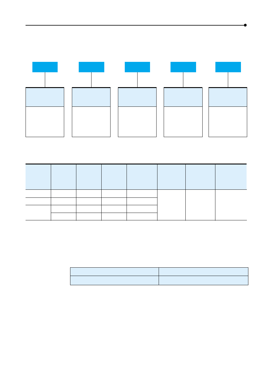
Code
Designation
Type L W H I
1
I
2
RC1005(1/16W )
RC1608(1/10W)
RC2012( 1/8W )
RC3216( 1/4W)
RC3225( 1/4W )
RC5025( 1/2W )
RC6432( 1W )
1.00
±0.05
1.60
±0.10
2.00
±0.20
3.20
±0.20
3.20
±0.20
5.00
±0.15
6.30
±0.15
0.50
±0.05
0.80
±0.15
1.25
±0.15
1.60
±0.15
2.55
±0.20
2.50
±0.15
3.20
±0.15
0.35
±0.05
0.45
±0.10
0.50
±0.10
0.55
±0.10
0.55
±0.10
0.55
±0.15
0.55
±0.15
0.20
±0.10
0.30
±0.20
0.40
±0.20
0.45
±0.20
0.45
±0.20
0.60
±0.20
0.60
±0.20
0.25
±0.10
0.35
±0.10
0.35
±0.20
0.40
±0.20
0.40
±0.20
0.60
±0.20
0.60
±0.20
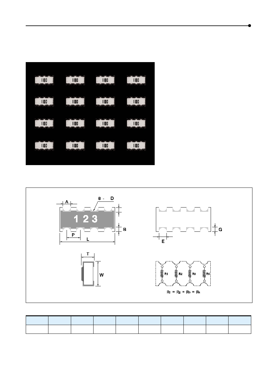
STRUTURE AND DIMENSIONS
PARTS NUMBERING SYSTEM
T
TH
HIIC
CK
K F
FIIL
LM
M C
CH
HIIP
P R
RE
ES
SIIS
ST
TO
OR
RS
S
Glass Coating
Alumina Substrate
Special Plating
H
L
W
l
2
l
2
l
1
l
1
Thick-Film Electrode
RuO
2
Type Resistor
Chip
Resistor
-RC
:Glass Coating
-RH
:Polymer Epoxy
Coating
R C
1
Dimension
(mm)
1005 : 1.0
◊0.5
1608 : 1.6
◊0.8
2012 : 2.0
◊1.25
3216 : 3.2
◊1.6
3225 : 3.2
◊2.55
5025 : 5.0
◊2.5
6432 : 6.4
◊3.2
2012
2
Resistance
Tolerance
D :
±0.5%
F :
±1 %
G :
± 2 %
J :
± 5 %
K :
±10%
J
3
Resistance Value Marking
3 or 4 digit coding system.
(IEC Coding System)
Resistance Value
1st two digits represents
Significant figures.
The last digit represents
the number of zeros.
Jumper chip is
represented as 000
100
4
Packaging Code
AS : Tape
Packaging. 13
"
CS: Tape
Packaging. 7
"
ES : Tape
Packaging. 10
"
BS :Bulk
Packaging.
CS
5
(UNIT : mm)
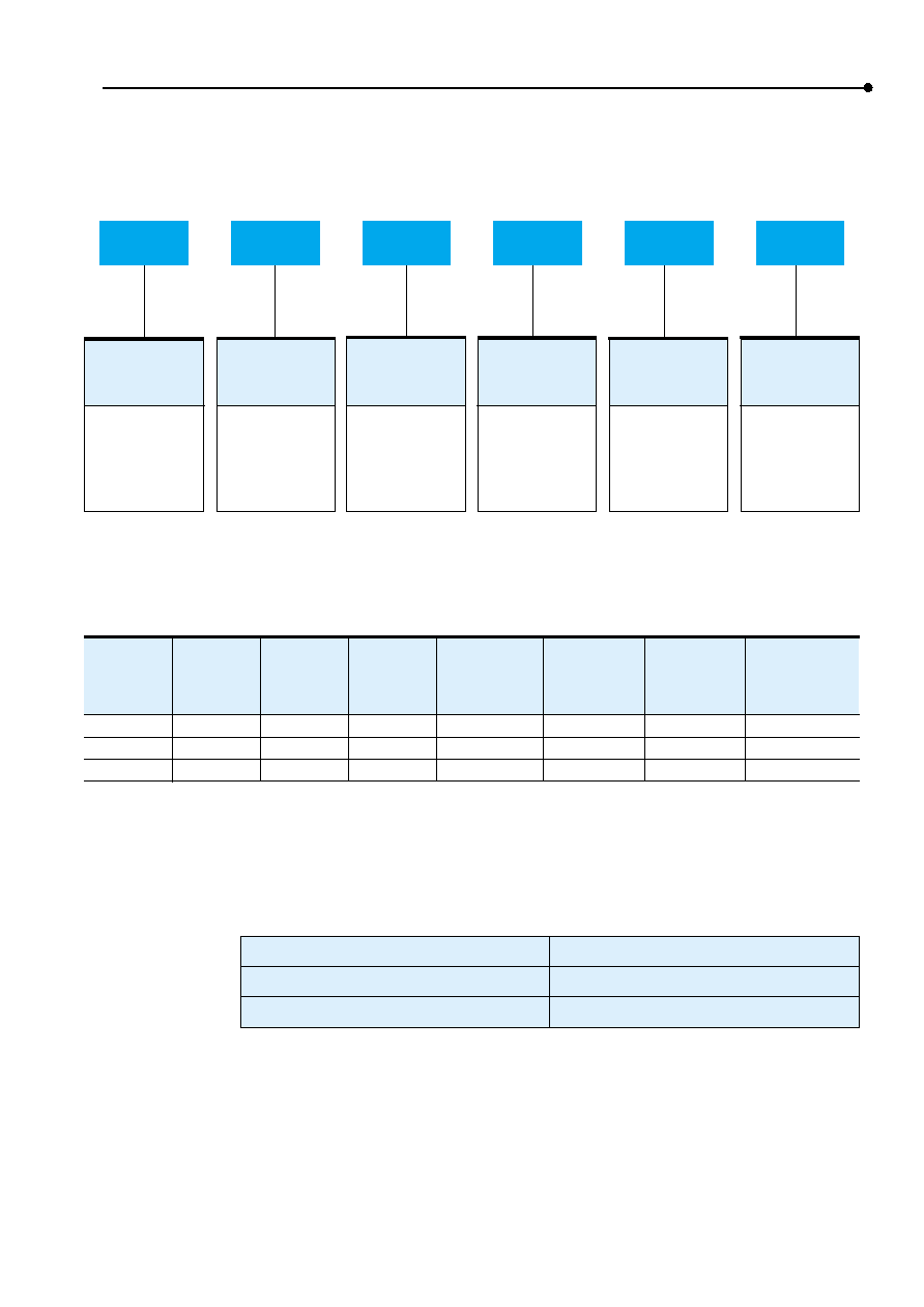
4
Descripition
Working Voltage(Max)
Power Derating Curve
Rated Voltage
Resistance Range
Overload Voltage(Max)
50V
100V
50V
100V
50V
100V
150V
300V
200V
400V
200V
400V
200V
400V
200V
400V
RC1005
RC1608
RC2012
RC3216
RC5025
RC6432
Power Rating (W)
at 70
0.063W
0.10W
0.125W
RC3225
0.25W
0.25W
0.5W
1W
D(
±
0.5%)
F(
±
1%), G(
±
2%)
J(
±
5%)
K(
±
10%)
Jumper Chip
-
10~1M
10~1M
10~1M
-
10~1M
1~10M
1~10M
-
10~1M
1~10M
1~10M
-
10~1M
1~10M
1~10M
10~1M
10~1M
1~10M
1~10M
10~1M
10~1M
1~10M
1~10M
10~1M
10~1M
1~10M
1~10M
10~1M
10~1M
1~10M
1~10M
50
m
max
-55
~ 125
-55
~ 155(For 1608, 2012, 3216)
70
Operating
Temperature Range
Rated
Temperature Range
100
80
60
40
20
-40
40
0
80
120
0
GENERAL SPECIFICATION
T
TH
HIIC
CK
K F
FIIL
LM
M C
CH
HIIP
P R
RE
ES
SIIS
ST
TO
OR
RS
S
5
The rated power is the maximum continuous loading power
at 70
ambient temperature.
For ambient temperature's above 70
the loading power
follows the above power derating curve.
Rated power(w)
◊Normal resistance value (W)
(UNIT :
)
Temperature
Coefficient
Resistance Range
Resistance
Tolerance
J (
±5%)
K (
±10%)
G (
±2%)
F (
±1%)
D (
±0.5%)
1
R10
10
R
2
1
1
R
2
10
10
R
2
1
Temperature Coefficient
±(300/200) PPM/
±100 PPM/
±3 00 PPM/
±100 PPM/
Please specify wattage when power rathing at the mark( ) is required at the time of ordering.
100
80
60
40
20
-5
-55
55 70
105
155
0
1608, 2012, 3216
Descripition
Working Voltage(Max)
Power Derating Curve
Rated Voltage
Resistance range
Overload Voltage(Max)
50V
100V
200V
200V
200V
100V
200V
400V
400V
400V
RC2012
Power Rating (W)
at 70
0.10W
RC3216
0.125W
0.25W
RC3225
0.25W
RC5025
0.5W
RC6432
1W
F(
±
1%)
G(
±
2%)
J(
±
5%)
K(
±
10%)
0.2
~
0.91
(E24 Series)
-55
~ 125
70
Operating
temperature range
Rated
Ambient Temperature
100
80
60
40
40
-40
-20
0
20
40
80
100
120 125 140
0
SPECIFICATION IN THE LOW RESISTANCE RANGE
POWER Derating Curve
6
The rated power is the maximum continuous loading power
at 70
ambient temperature.
For ambient temperature's above 70
the loading power
follows the above power derating curve.
Rated power(w)
◊Normal resistance value (W)
(UNIT :
)
Temperature
Coefficient
Resistance Range
Resistance
Tolerance
0.2
R1
Temperature Coefficient
±200 PPM/
0.2
R1
±200PPM/
0.2
R1
±(600/300)PPM/
0.2
R1
±(600/300)PPM/
F(
±1%)
G(
±2%)
J(
±5%)
K(
±10%)
Please specify wattage when power rathing at the mark( ) is required at the time of ordering.
T
TH
HIIC
CK
K F
FIIL
LM
M C
CH
HIIP
P R
RE
ES
SIIS
ST
TO
OR
RS
S
7
TYPE L W H I
1
I
2
X Y
RT1608 1.60
±0.10 0.80±0.15 0.45±0.10 0.30±0.20 0.35±0.10 0.50±0.10 0.40±0.10
RT2012 2.00
±0.20 1.25±0.15 0.50±0.10 0.40±0.20 0.35±0.20 0.70±0.10 0.60±0.10
RT3216 3.20
±0.20 1.60±0.15 0.55±0.10 0.45±0.20 0.40±0.20 1.30±0.10 1.00±0.10
(Unit : mm)
T
TH
HIIC
CK
K F
FIIL
LM
M C
CH
HIIP
P R
RE
ES
SIIS
ST
TO
OR
RS
S
TRIMMABLE CHIP RESISTOR
FEATURES
Available in use of function trimming.
Compatible with both wave and reflow
soldering.
Highly stable in auto-placement surface
mounting application.
Excellent eletrical characteristic.
X, Y : Trimming area
DIMENSIONS
8
GENERAL SPECIFICATION
T
TH
HIIC
CK
K F
FIIL
LM
M C
CH
HIIP
P R
RE
ES
SIIS
ST
TO
OR
RS
S
Code
Designation
PACKAGING
The Chip Network Resistors can be supplied with packaged carrier tape for effective use in SMD machine.
All Reel taping specifications are in accordance with EIAJ RC-1009.
Standard Quantity :
Chip Resistor for Bulk shall be in the polyethylene bag and Quantity of the
Chip Resistors in bag is determined by customer orders.(Standard Quantity : 5,000EA)
RATING
Type
Power
Rating
Working
Voltage
(MAX)
Over Ioad
Voltage
(MAX)
Resistance
Range
Operting
Temperature
Range
Rating
Ambient
Temperature
Temperature
Coefficient
RT1608
1/16 W
50 V
100 V
1~10
RT2012
1/10W
100 V
200 V
1~10
RT3216
1/8W
200 V
400 V
1~10
1/4W
200 V
400 V
1~10
-55
~ +125
+70
±200ppm/
±300ppm/
7 inch reel 5,000/1 reel
13 inch reel
20,000/1 reel
RT:DIP Type(Major)
RT
Code
Designation
Trimmable
Chip
Resistor
Code
Designation
2012
Dimension
(mm)
1608:1.6
◊0.8
2012:2.0
◊1.25
3216:3.2
◊1.6
Code
Designation
M
Resistance
Tolerance
K =
±10%
Code
Designation
100
Resistance
Value
E12 Series
E6 Series
(IEC Coding system)
Code
Designation
CS
Packaging
Code
CS : Tape
Packaging
GS : Bulk
Packaging

9
T
TH
HIIC
CK
K F
FIIL
LM
M C
CH
HIIP
P R
RE
ES
SIIS
ST
TO
OR
RS
S
R
/
R TYPE CHIP NET WORK RESISTOR
FEATURES
High density mouting
Improvement of placement efficiency.
Automatic placement.
DIMENSIONS
TYPE L W T A D B P E G
RR164P 3.2
±0.2 1.5±0.2 0.5±0.2 0.5±0.2 Max 0.16 0.25±0.2 0.8±0.15 0.5±0.2 0.25±0.2
UNIT [mm]
10
TYPE L W T A D B P E G
RN164P 3.2
±0.2 1.6±0.2 0.6±0.1 0.45±0.1 0.3±0.1 0.3±0.2 0.8±0.1
0.45
±0.1 0.40±0.15
UNIT [mm]
T
TH
HIIC
CK
K F
FIIL
LM
M C
CH
HIIP
P R
RE
ES
SIIS
ST
TO
OR
RS
S
R
/
R TYPE CHIP NET WORK RESISTOR
FEATURES
High density mouting
Improvement of placement efficiency.
Automatic placement.
DIMENSIONS
11
T
TH
HIIC
CK
K F
FIIL
LM
M C
CH
HIIP
P R
RE
ES
SIIS
ST
TO
OR
RS
S
7 inch reel
5,000EA/1 reel
PARTS NUMBERING SYSTEM
Code
Designation
Chip Network
Resistor
Dimension
(mm)
Number
of Resistors
4p : 4 Resistors
Resistance
Tolerance
G :
±2%
J :
±5%
K :
±10%
Resistance
Value
E24 Series
(IEC Coding system)
Packaging
Code
PACKAGING
The Chip Network Resistors can be supplied packaged carrier tape for effective use SMD machine.
All Reel taping specifications are in accordance with EIAJ RC-1009.
Standard Quantity :
Chip Network Resistor for Bulk shall be in the plastic case and Quantity of the Chip Resistors in bag is
determined by customer orders.(Standard Quantity : 5,000EA)
RATING
Type
Power
Rating
Working
Voltage
(MAX)
OverIoad
Voltage
(MAX)
Resistance
Range
Operting
Tempe rature
Range
Rating
Ambient
Temperature
Temperature
Coefficient
RP104P
1/16W
50V
100V
10~1M
-55 ~ 125
+70
±250 PPM/
RP164P
1/16W
50V
100V
10~1M
-55 ~ 125
+70
±250 PPM/
RN164P
1/16W
50V
100V
10~1M
-55 ~ 125
+70
±250 PPM/
10 inch reel
10,000EA/1 reel
13 inch reel
20,000EA/1 reel(15,000EA/1reel)
RP/RN
16/10
J
103
CS
4P
16:1608 Type
10:1005 Type
CS/AS/ES :
Tape
Packaging
GS : Bulk
Packaging
RP, RR : Dip Type(Convex Type)
RN : Through Hole Type(Concave Type)
12
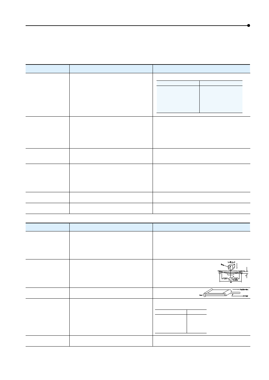
Coverage : 95% each termination.
Visual : No crack of termination parts and
ceramic exposure of surface by melting
After immersing in flux. dip into the 235
±5 molten
solder for 2
±0.5 sec
Solder : S63A(KSD 6704)
Flux : ROSIN(KSM 2951)
Flux is the composition of ROSIN and the methanol Weight
rate of ROSIN is about 25%
Solderability
Bending Test
R : ±(0.5%+0.05) of the initial value
Visual : No evidence of mechanical damage.
After soldering resistor on the
PCB, 3mm of bending shall
be applied for 10 sec.
Material of PCB : Glass Epoxy
Thickness : 1.6mm
Measure resistance during load application
Terminal Strenght
Load pull : 0.5kg
1005(1/16W), 1608(1/16W) 0.3kg
pull Direction fixed 0.4 lead
Terminal Strenght
R : ±(1%+0.05) of the initial value
Visual : No evidence of mechanical damage.
Anti-Vibration Test
R : ±(1%+0.05) of the initial value
Visual : No evidence of mechanical damage.
Immerse in molten solder at 260
±5 for 10±1 sec.
Preheat and soldering Procedure
2 hours each in X, Y, and Z axis(toyal 6 hours) 10 to
55 Hz sweep in 1 minute ampiltude.
Item
Specification
Test Method
CHARACTERISTICS PERFORMANCE
ELECTRICAL CHARACTERISTICS
MECHANICAL CHARACTERISTICS
T
TH
HIIC
CK
K F
FIIL
LM
M C
CH
HIIP
P R
RE
ES
SIIS
ST
TO
OR
RS
S
Direct Current
Resistance
Within the regulated resistance tolerance.
Jumper chip 50
1 R 10:+300ppm/
-200ppm/
10 R 1M:
±100ppm/
1M R 10M:
±300ppm/
R : ±(1%+0.1) of the initial value
Visual : No evidence of mechanical damage
Jumper chip : 50
Apply 2.5 times rated voltage for 5sec.
Wait 30 minutes at room temperature and measure the
resistance value.
R : ±(3%+0.1) of the initial value
Visual : No evidence of mechanical damage
Jumper chip : 50
No evidence of mechanical damage.
Apply AC 500V for 1 minute.
1005(1/16W), 1608(1/16W):Apply AC 100V for 1 minute
Over the 1000
Apply DC 500V for 1 minute.
1005(1/16W), 1608(1/16W):Apply DC 100V for 1 minute
Perform 10,000 cycles at 2.5 times RCW or the Max.
over load voltage
ON(2.5 times rated volage) : 1 sec
OFF : 25 sec
Have stabilization time of 30 minutes without loading
and measure resistance.
Test temperature(
) (20) (-55) (20) (125) (20)
T.C.R(ppm/
) = (R-Ro)/Ro◊1/(T-To) ◊10
6
T = 20(
)
T = Test temperature(
)
Ro = Resistance at room temperature(
)
R = Resistance at T(
)
Applying time:within 5 sec
T.C.R(Resistance
Temperature
Characteristic)
Short-time Overload
Intermittent
Overload
Dielectric withstand-
ing Voltage
Insulation Resistance
Item
Specification
Test Method
Resistance range(
)
R 100
100
R 1K
1K R 10K
10K R 100K
100K R 1M
1M R
Max test voltage(V)
0.3
1.0
3
10
25
50
Solder : S63A(SSD 6704)
Flux : The composition of ROSIN
(KSM295)25% and methanol
(KSM 1658)75%
Temperature(
)
Time(sec)
80 - 100
150 - 180
260 + 5
150 - 180
80 - 100
120
120
10
60
60
13
ELECTRICAL CHARACTERISTICS
Low Temperature
exposure
R : ±(3%+0.1) of the initial value.
Visual : No evidence of mechanical damage.
Dwell in -55
chamber without loading for 1000±12 hours
Dwell for 60 minutes at Room temperature and
Measure resistance value.
Temperature Cycle
R : ±(1%+0.1) of the initial value.
Visual : No evidence of mechanical damage.
Perform 100Cycles as follows.
Load Life in
Moisture
Temperature : 40
±2
RH : 90~95%
Applying rated voltage for 90 minutes "ON" and
30minutes"OFF"
Duration : 1000 hours
Dwell in Room temperature for 1 hour and measure
resistance value.
No.
Temperature(
)
Time(min)
1
-55
±
3
30
2
20
±
3
15
3
125
±
3
30
4
20
±
3
15
Item
Specification
Test Method
T
TH
HIIC
CK
K F
FIIL
LM
M C
CH
HIIP
P R
RE
ES
SIIS
ST
TO
OR
RS
S
At R 10
R :
±5%
At R 1
R :
±(3% + 0.1)
At R 1
R :
±5%
Visual : No evidence of mechanical damage.
Load Life in high
Temperature
Temperature : 70
±3 at rated voltage.
Applying rated voltage for 90 minutes "ON" and
30minutes"OFF"
Duration : 1000 hours
Dwell in Room temperature for 1 hour and measure
resistance value.
At R 10
R :
±5%
At R 1
R :
±(3% + 0.1)
At R 1
R :
±5%
Heat Resistance
(High Temperature
Exposure)
Dwell in 125
±3 chamber without loading for
1000
±12 hours
Dwell in Room temperature for 1 hour and measure
resistance value.
R : ±(3%+0.1) of the initial value.
Visual : No evidence of mechanical damage.
14
T
TH
HIIC
CK
K F
FIIL
LM
M C
CH
HIIP
P R
RE
ES
SIIS
ST
TO
OR
RS
S
WINDOW DIMENSIONS
A
B
t
0.7
±
0.10
1.20
±
0.10
0.5(MAX)
2.80
5.32
±
0.20
1.10(MAX)
3.50
±
0.10
6.75
±
0.10
1.10(MAX)
RC 1005
(1/16W)
RC 5025
(1/2W)
RC 6432
(1W)
SIGN.
ITEM
(mm)
PACKAGING
The Chip Resistor can be supplied with packaged carrier tape for effective use in SMD machine.
All Reel taping specifications are in accordance with EIAJ RC-1009.
Standard Quantity :
Chip Resistor for Bulk shall be in the plastic Quantity of the
Chip Resistors in bag is determined by custom orders.(Standard Quantity : 5,000EA)
7 inch reel
10 inch reel
-
10,000EA/1 reel
-
13 inch reel
10,000EA/1 reel
40,000EA/1 reel
5,000EA/1 reel
20,000EA/1 reel
4,000EA/1 reel
15,000EA/1 reel
REEL SIZE
1608, 2012, 3216
5025, 6432
1005
CARRIER TAPE DIMENSIONS
This is applied to 1005 series.
This is applied to 5025, 6432 series.
(Unit: mm)
Chip Resistor
Bottom Tape
Carrier Tape
Top Tape
4.0
±0.1
4.0
±0.1
1.75
±0.1
1.75
±0.1
3.5
±0.05
5.5
±0.05
8.0
±0.1
12.0
±0.3
1.5
±
0.1
0
1.5
±
0.1
0
2.0
±0.05
1.0
1.0
t
t
A
2.0
±0.05
4.0
±0.1
A
t=0.5~1.0 Max
Chip Resistor
Embossed Carrier
Top Tape
t=1.1 Max
B
15
T
TH
HIIC
CK
K F
FIIL
LM
M C
CH
HIIP
P R
RE
ES
SIIS
ST
TO
OR
RS
S
(Unit: mm)
This is applied to 1608, 2012, 3216, 3225 series
WINDOW DIMENSIONS
TAPING METHOD
REEL DEMENSIONS
A
B
t
1.10
±
0.20
1.90
±
0.20
0.90(MAX)
RC 1608
(1/16W)
1.65
±
0.20
2.40
±
0.20
1(MAX)
RC 2012
(1/10W)
2.00
±
0.20
3.60
±
0.20
1(MAX)
RC 3216
(1/8, 1/4W)
2.90
±
0.20
3.60
±
0.20
1(MAX)
RC 3225
(1/4W)
SIGN.
ITEM
(mm)
(
178mm : 7 inch)
(
330mm : 13 inch)
Chip Resistor
Bottom Tape
Carrier Tape
Top Tape
4.0
±0.1
1.75
±0.1
3.5
±0.05 8.0±0.1
1.5
±
0.1
0
2.0
±0.05
4.0
±0.1
1.0
1.0 Max
A
1.0 Max
B
Reel
Packed Part
Empty Part
Lead Part
Adhesion Tape
Empty portion
10 Pitches
or more
5,000 Pitches
or 20,000 Pitches
10 Pitches
or more
200~250 mm
Chips
Empty portion
Lead Part
Start
End
1.2
±0.1
ÿ
178
±
1.0
ÿ
13
±
1.0
ÿ
70
±
1.0
9.5
±0.1
or
13
±0.1
2.0
±0.1
40
R6.5
20
ÿ
330
±
1.0
ÿ
13
±
1.0
ÿ
80
±
1.0
9.0
±0.1
or
13
±0.1
R 165
R 145