
Raytheon RF Components
362 Lowell Street
Andover, MA 01810
Revised March 28, 2002
Page 1
www.raytheonrf.com
Characteristic performance data and specifications are subject to change without notice.
PRODUCT INFORMATION
The Raytheon RMLA3565A-58 is a single bias wideband low noise MMIC amplifier designed for the 3.5 - 6.5 GHz
frequency range. The MMIC requires no external matching circuits or external gate bias supply. This device uses
Raytheon's advanced 0.25 µm PHEMT process to provide low noise, high linearity, and low current.
Description
Absolute
Maximum
Ratings
1
Electrical
Characteristics
2
19.0 dB Gain typical
1.2 dB Noise Figure Typical 5.0 - 6.5 GHz
Single Positive Bias
Small Outline Metal Base Quad Plastic Package
Internal 50
Matching
Features
Notes:
1. No permanent damage with only one parameter set at maximum limit and all other parameters at typical conditions.
2. All parameters met at Tc = +25 ∞C, Vdd = 4.0V.
3. Pin = -20 dBm, Vdd = 4.0 V, Frequency 3.5 - 6.5 GHz
4. Data de-embedded from fixture loss
RMLA3565A-58
Wideband Low Noise MMIC Amplifier
(Photo TBS)
Parameter
Symbol
Value
Unit
Positive Drain DC Voltage (No RF)
Vdd
6.5
V
RF Input Power (from 50
source)
Pin(CW)
0
dBm
Drain Current
Idd
130
mA
Case Operating Temperature
Tc-35 to 85
∞C
Storage Temperature Range
Tstg
-40 to 110
∞C
Soldering Temperature
Tsolder
220
∞C
Parameter
Min
Typ
Max
Unit
Frequency Range
3.5
6.5
GHz
Gain (Small Signal)
3,4
17.0
19.0
dB
Gain Variation vs Temp
-0.008
dB/∞C
Noise Figure
4
3.5 - 5 GHz
1.4
1.9
dB
5 - 6.5 GHz
1.2
1.4
dB
Power Out, P1dB @ 5.5 GHz 8.0
10.0
dBm
Parameter
Min
Typ
Max
Unit
OIP3 @ 5.5 GHz, +3 dBm
Pout total
17
21.0
dBm
Idd
70.0
85.0
mA
Vdd
3.0
4.0
6.0
V
Input Return Loss
-15.0
dB
Output Return Loss
-10.0
dB
Thermal Resistance Rjc
135
∞C/W
(Channel to Case)
Raytheon RF Components
362 Lowell Street
Andover, MA 01810
Revised March 28, 2002
Page 2
www.raytheonrf.com
Characteristic performance data and specifications are subject to change without notice.
PRODUCT INFORMATION
CAUTION: THIS IS AN ESD SENSITIVE DEVICE
The following briefly describes a procedure for evaluating the high efficiency PHEMT amplifier packaged in a
surface mount package. It may be noted that the chip is a fully monolithic single ended two stage amplifier for 3.5
to 6.5 GHz applications.
Test Fixture
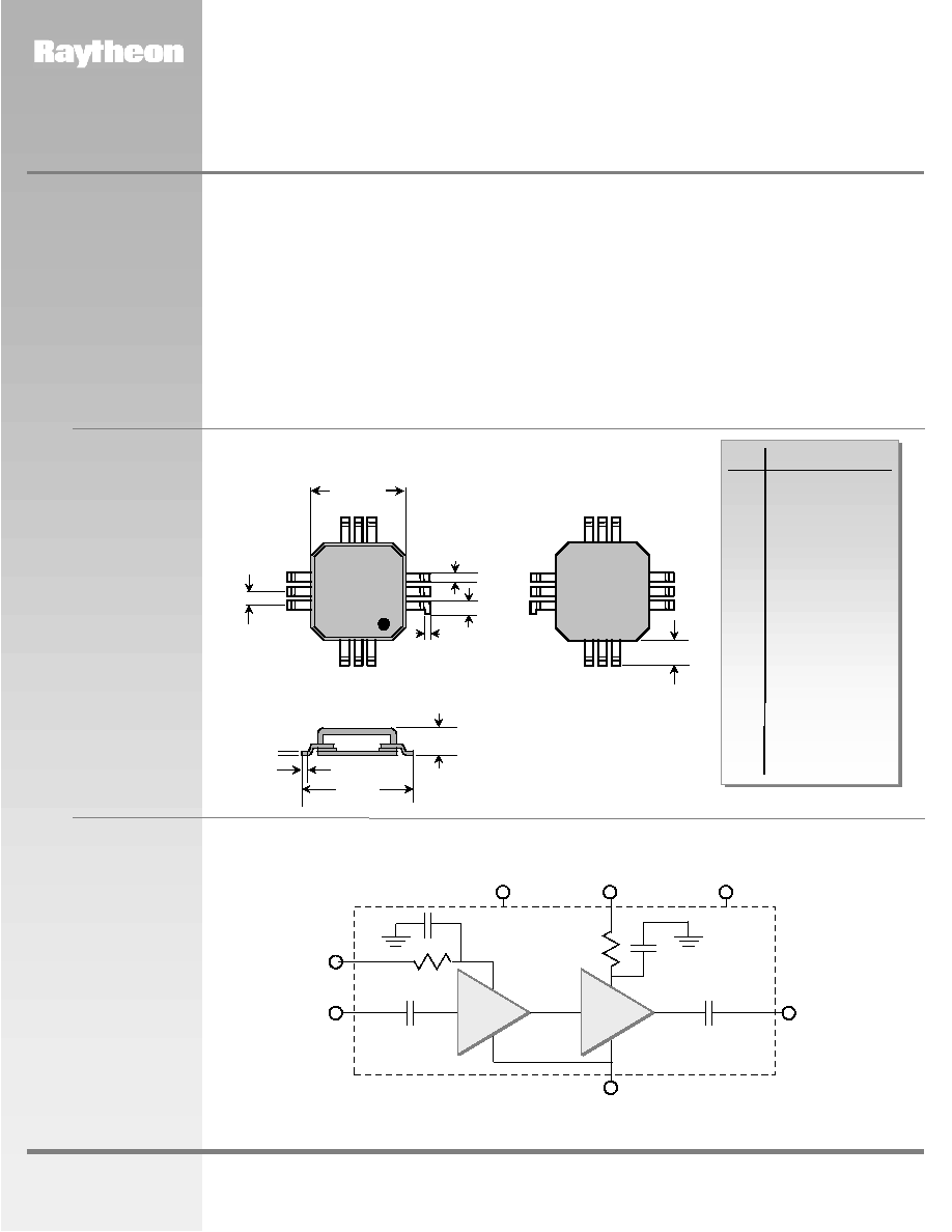
Figure 1 shows the outline and pin-out descriptions for the packaged device. Figure 2 shows the functional block
diagram of the packaged product. A typical test fixture schematic showing external bias components is shown in
Figure 3. Figure 4 shows typical layout of an evaluation board corresponding to the schematic diagram. Typical
performance of the test fixture is shown in the performance data section. The following should be noted:
(1) Package pin designations are shown in figure 1.
(2) Vd is the drain voltage (positive) applied at the pins of the package.
(3) Vdd is the positive supply voltage at the evaluation board terminal.
Application
Information
RMLA3565A-58
Wideband Low Noise MMIC Amplifier
Figure 1
Package Outline and
Pin Designations
Dimensions in inches
Figure 2
Functional Block
Diagram
Pin#
Description
1
N/C
2
RF Out
3
GND
4
N/C
5
GND
6
N/C
7
GND
8
RF In
9
N/C
10
N/C
11
N/C
12
Vd
13
GND
(Package Base)
PLASTIC LID
SIDE SECTION
0.075 MAX.
0.008
1
2
3
5
4
6
7
9
8
10
12 11
0.041
1
3
0.200 SQ.
TOP VIEW
TOP VIEW
BOTTOM VIEW
5 4
6
7
9
8
10
12
11
0.030
0.015
0.282
2
0.015
0.020
0.011
RF OUT
Pin# 2
N/C
1,4,6,9,10,11
(Recommend grounding
externally to PC board)
Vd
Pin# 12
Ground
Pin# 5
Ground
Pins# 3,5,7,13
RF IN
Pin# 8
Ground
Pin# 7
Raytheon RF Components
362 Lowell Street
Andover, MA 01810
Revised March 28, 2002
Page 3
www.raytheonrf.com
Characteristic performance data and specifications are subject to change without notice.
PRODUCT INFORMATION
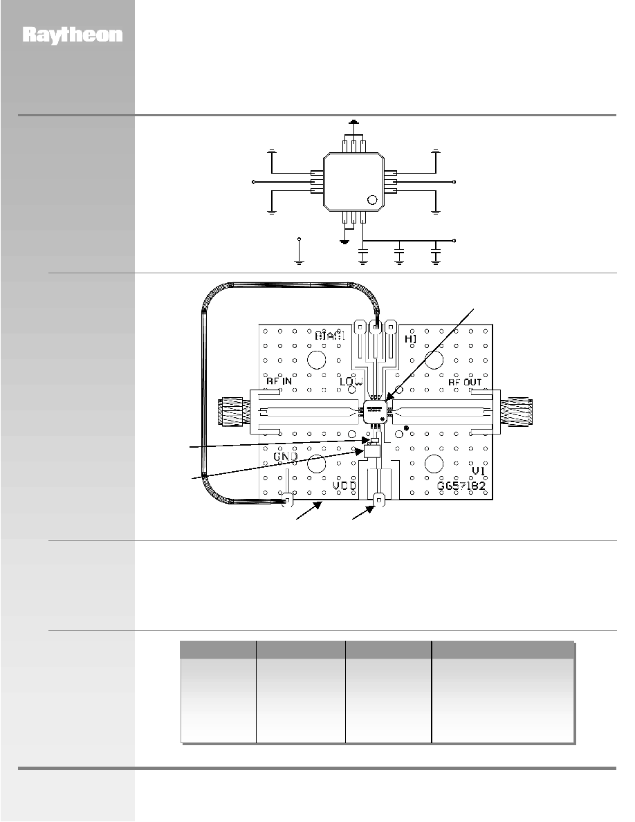
Figure 4
Layout and Assembly of
Test Evaluation Board
(RMLA3565A-58-TB)
RMLA3565A-58
Wideband Low Noise MMIC Amplifier
Figure 3
Schematic for a Typical
Test Evaluation Board
(RMLA3565A-58-TB)
The following sequence of procedure must be followed to properly test the power amplifier:
Test Procedure
for the evaluation board
(RMLA3565A-58-TB)
Step 1: Turn off RF input power.
Step 2: Use GND terminal of the evaluation board to
connect DC supply grounds.
Step 3: Apply drain supply voltage of +4.0 V to
evaluation board terminal Vdd.
Step 4: After the bias condition is established, RF input
signal may now be applied.
Step 5: Follow turn-off sequence of:
(i) Turn off RF input power.
(ii) Turn down and off Vdd.
Parts List
for test evaluation board
RMLA3565A-58-TB
Part
Value
EIA Size
Vendor(s)
C1
330 pF
.04" x .02"
AVX, Murata, Novacap,
C2
4.75 uF
.14"x .11"
Sprague, ATC, AVX, Murata
U1
RMLA3565A-58
.28" x .28" x .07"
Raytheon
P1, P2
Terminal
Samtec
J1, J2
SMA Connectors
E.F. Johnson
Board
RO4003(Rogers)
1.99x1.50x.032
Raytheon
C1
(Opt)
C2
(OPT)
C3
Vdd
P1
RF in
J1
RF out
J2
GND
P2
Ray
LA3565
RF Out
J2
U1
RF In
J1
C1
C2
Ground
(GND) P2
Vdd P1
Raytheon RF Components
362 Lowell Street
Andover, MA 01810
Revised March 28, 2002
Page 4
www.raytheonrf.com
Characteristic performance data and specifications are subject to change without notice.
PRODUCT INFORMATION
RMLA3565A-58
Wideband Low Noise MMIC Amplifier
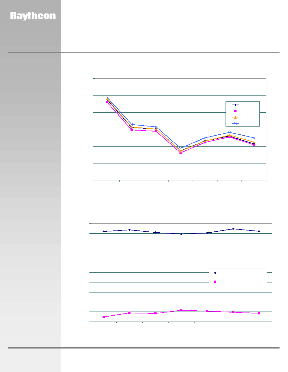
0.80
1.00
1.20
1.40
1.60
1.80
2.00
3.5
4
4.5
5
5.5
6
6.5
Frequency (GHz)
NF
(
d
B
)
NF (3V)
NF (4V)
NF (5V)
NF (6V)
Performance
Data
RMLA3565A-58
Noise Figure Vs Frequency for Vdd from 3 Vdc to 6 Vdc (25∞C)
-0.5
-0.4
-0.3
-0.2
-0.1
0
0.1
0.2
0.3
0.4
0.5
3.5
4
4.5
5
5.5
6
6.5
Frequency (GHz)
NF
(d
B)
Hot (85 deg C) minus Ambient
Cold (-35 deg C) minus Ambient
RMLA3565A-58
Noise Figure (4Vdc) Change Vs Temperature
Raytheon RF Components
362 Lowell Street
Andover, MA 01810
Revised March 28, 2002
Page 5
www.raytheonrf.com
Characteristic performance data and specifications are subject to change without notice.
PRODUCT INFORMATION
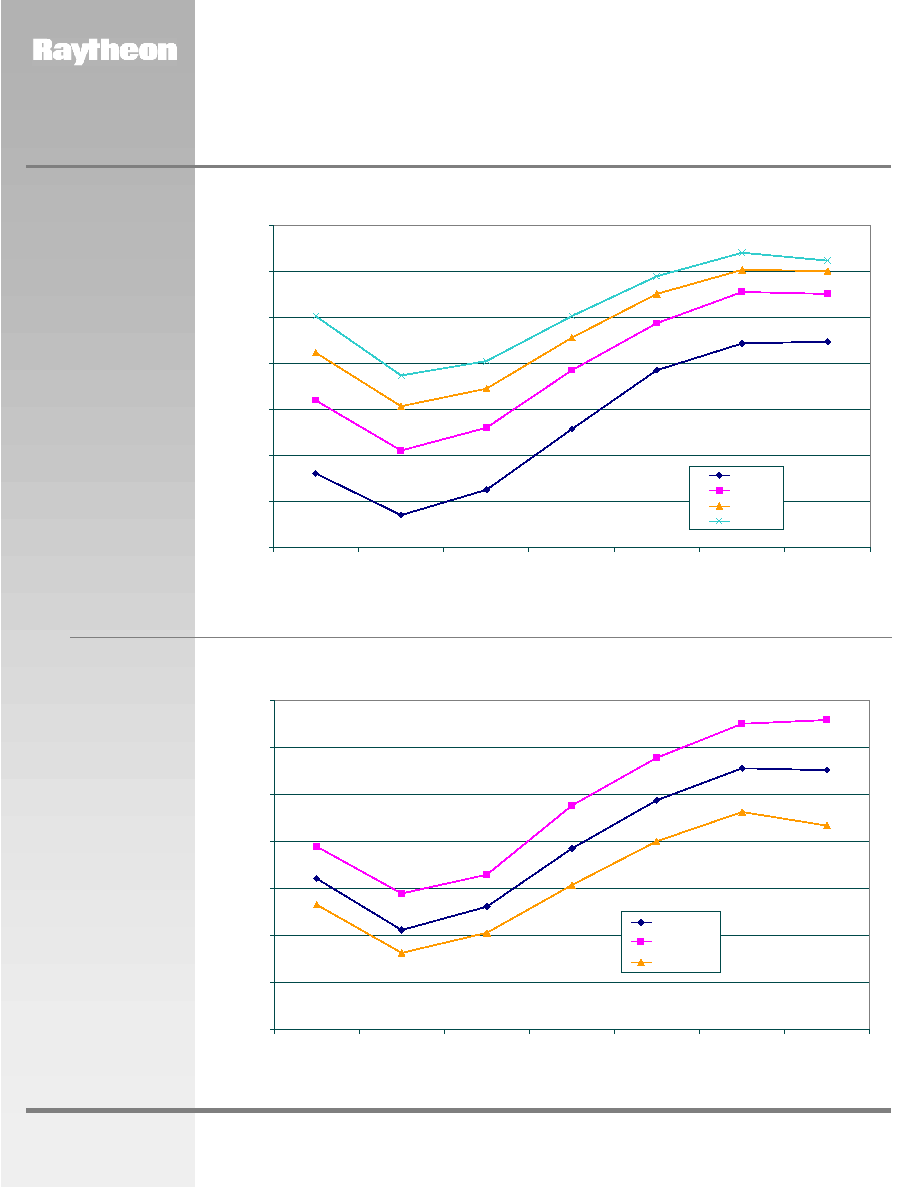
17
17.5
18
18.5
19
19.5
20
20.5
3.5
4
4.5
5
5.5
6
6.5
Frequency (GHz)
S2
1
(
d
B
)
25 deg C
- 35 deg C
85 deg C
RMLA3565A-58
Small Signal Gain (Vdd = 4 Vdc) Vs Temperature and Frequency
17
17.5
18
18.5
19
19.5
20
20.5
3.5
4
4.5
5
5.5
6
6.5
Frequency (GHz)
S
21 (
d
B
)
3 Vdc
4 Vdc
5 Vdc
6 Vdc
Performance
Data
RMLA3565A-58
Small Signal Gain (Tcase = 25∞C) Vs Vdd and Frequency
RMLA3565A-58
Wideband Low Noise MMIC Amplifier