
RT9173/A
November, 2000
RichTek Technology Corp.
DS9173/A-00
6F, No. 35, Hsintai Road, Chupei City, Hsinchu, Taiwan, R.O.C.
Tel: (8863) 5510047 Fax: (8863) 5537749
-- 1 / 5 --
3A Bus Termination Regulator
General Description
The RT9173/A regulator is designed to convert
voltage supplies ranging from 1.8V to 6V into a
desired output voltage which adjusted by two
external resistors, voltage divider. The regulator
is capable of sourcing or sinking up to 3A of
current while regulating an output voltage to
within 2% or less.
The RT9173/A, used in conjunction with series
termination resistors, provides an excellent
voltage source for active termination schemes of
high speed transmission lines as those seen in
high speed memory buses and distributed
backplane designs. The voltage output of the
regulator can be used as a termination voltage
for DDR.
Features
� Power TO-263-5 Package.
� Capable of Sourcing and Sinking Current 3A
� Current-limiting Protection
� Thermal Protection
� Integrated Power MOSFETs.
� Generates Termination Voltages for SSTL-2
� High Accuracy Output Voltage at Full-load
� Adjustable VOUT by External Resistors
� Minimum External Components
� Shutdown for Standby or Suspend Mode
Operation with High-impedance Output
� Soft-start Function
Applications
� Computers
� Disk Drives
� CD-ROM
� Supply Splitter
Ordering Information
RT9173/A
Pin Configuration
Part Number
Pin Configuration
Pin
Name
1
VIN
2
GND
3 VCNTL
4
REFEN
5
VOUT
RT9173/ACM5
(Plastic TO-263-5)
Absolute Maximum Ratings
� Input Voltage Range
7V
� Power Dissipation
Internally Limited
� ESD Rating
3KV
� Storage Temperature Range
-50
�C to 150�C
� Lead Temperature (Soldering, 5 seconds)
260
�C
� Package Thermal Resistance
TO-263 (
JC
)
2
�C/W
Package type
M5: TO-263-5
Operation temperature range
C: Commercial standard
3A sink & source
1A sink & source
1 2 3 4 5
MARK

RT9173/A
November, 2000
RichTek Technology Corp.
DS9173/A-00
6F, No. 35, Hsintai Road, Chupei City, Hsinchu, Taiwan, R.O.C.
Tel: (8863) 5510047 Fax: (8863) 5537749
-- 2 / 5 --
Electrical Characteristics
Limits in standard typeface are for T
J
= 25
�C, unless otherwise specified:
VIN = 2.5V, VCNTL = 3.3V, V
REFEN
= 1.25V, C
OUT
= 10
�F (Ceramic)
Parameter
Test Conditions
Min. Typ. Max. Units
Output Offset Voltage, V
OS
Figure 1.
-15
0
15
mV
Load Regulation,
V
OUT
I
L
: -3A 3A, Figure 1.
-2
0
+2
%
VIN
1.8
2.5
6
V
Input Voltage Range
VCNTL
Keep VCNTL
VIN in operation
power on and power off sequences
3.3
6
V
Current In Shutdown Mode, I
SHDN
V
REFEN
< 0.4V, RL = 10K, Figure 2.
30
60
�A
RT9173
1.5
3
Peak Output Current
RT9173A
3.5
5
A
Short Circuit Protection
RT9173
Figure 3,4
1.5
2
Current Limit, I
CL
RT9173A
Figure 3,4
3.5
4
A
Over Temperature Protection
Shutdown Threshold
150
�C
Thermal Shutdown Hysteresis
Guaranteed by design
50
�C
Shutdown
Function
Output = High, Figure 5
0.8
Shutdown threshold trigger
Output = Low, Figure 5
0.4
V
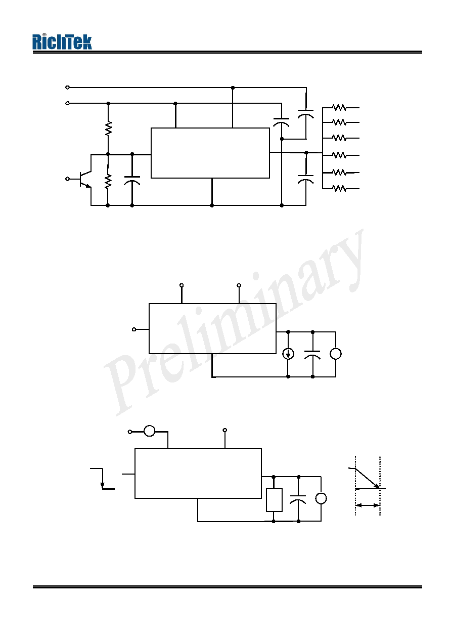
Function Block Diagram
Pin Description
Pin Name
Pin Function
VIN
Input Supply
GND
Ground
VCNTL
Gate Drive Voltage
REFEN
Reference Voltage Input and Chip Enable
VOUT
Output Voltage (equals to � VIN if R
1
= R
2
.)
VCNTL
Thermal
Current
Limiting Sensor
VOUT
EN
GND
CNTL
VIN
RT9173/A
November, 2000
RichTek Technology Corp.
DS9173/A-00
6F, No. 35, Hsintai Road, Chupei City, Hsinchu, Taiwan, R.O.C.
Tel: (8863) 5510047 Fax: (8863) 5537749
-- 3 / 5 --
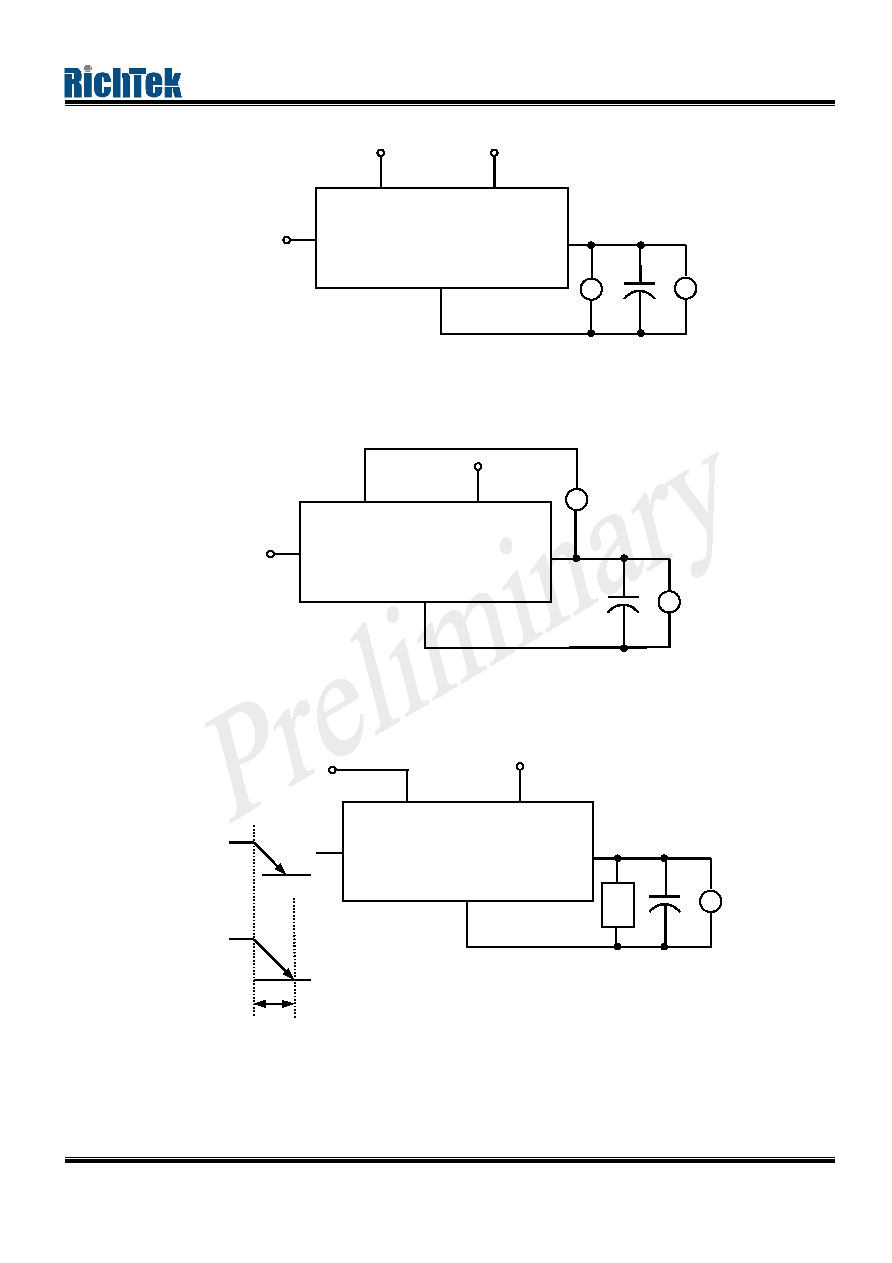
Typical Applications
R
1
= R
2
= 100K
, R
TT
= 50
/ 33 / 25
C
OUT
,
min
= 10
�F (ceramic), C
SS
= 1
�F, C
IN
= 100
�F, C
CNTL
= 47
�F
Test Circuits
Figure 1: Output Voltage Tolerance,
V
OUT
Figure 2: Current in Shutdown Mode, I
shcln
VIN VCNTL
REFEN
RT9173/A
VOUT
GND
1.25V
2.5V
3.3V
V
OUT
C
OUT
I
L
V
VIN VCNTL
REFEN
RT9173/A
VOUT
GND
R
TT
V
CNTL
= 3.3V
V
IN
= 2.5V
EN
R
2
C
SS
Q1
R
1
C
IN
C
OUT
C
CNTL
VIN VCNTL
REFEN
RT9173/A
VOUT
GND
1.25V
2.5V
3.3V
V
OUT
C
OUT
V
R
L
A
0.4V
0V
1.25V
R
L
and C
OUT
Time delay
RT9173/A
November, 2000
RichTek Technology Corp.
DS9173/A-00
6F, No. 35, Hsintai Road, Chupei City, Hsinchu, Taiwan, R.O.C.
Tel: (8863) 5510047 Fax: (8863) 5537749
-- 4 / 5 --
Figure 3: Current Limit for High Side, I
CLHIGH
Figure 4: Current Limit for Low Side, I
CLLOW
Figure 5: REFEN Pin Shutdown Threshold, V
trigger
VIN VCNTL
REFEN
RT9173/A
VOUT
GND
1.25V
2.5V
3.3V
V
OUT
C
OUT
I
L
V
A
Power supply
with current limit
VIN VCNTL
REFEN
RT9173/A
VOUT
GND
1.25V
2.5V
3.3V
V
OUT
C
OUT
V
A
I
L
VIN VCNTL
REFEN
RT9173/A
VOUT
GND
2.5V
3.3V
V
OUT
C
OUT
V
R
L
0.2V
0V
1.25V
1.25V
V
OUT
V
REFEN
R
L
and C
OUT
Time delay
V
OUT
would be low if VREFEN < 0.4V
V
OUT
would be high if VREFEN > 0.8V

RT9173/A
November, 2000
RichTek Technology Corp.
DS9173/A-00
6F, No. 35, Hsintai Road, Chupei City, Hsinchu, Taiwan, R.O.C.
Tel: (8863) 5510047 Fax: (8863) 5537749
-- 5 / 5 --
Package Information
Dimensions In Inches
Dimensions In Millimeters
Symbol
Min
Norm
Max
Min
Norm
Max
D
0.3921
0.4000
0.4079
9.96
10.16
10.36
B
0.0783
0.0862
0.0941
1.99
2.19
2.39
E
0.3307
0.3386
0.3465
8.40
8.60
8.80
A
0.1724
0.1803
0.1882
4.38
4.58
4.78
C
0.0465
0.0504
0.0543
1.18
1.28
1.38
L1
0.1169
0.1248
0.1327
2.97
3.17
3.37
L2
0.0602
0.0681
0.0760
1.53
1.73
1.93
b
0.0280
0.0319
0.0358
0.71
0.81
0.91
b2
0.0110
0.0150
0.0189
0.28
0.38
0.48
e
--
0.0669
--
--
1.70
--
5-Lead TO-263 Plastic Surface Mount Package
e
L2
B
MARK
D
E
L1
b
1 2 3
4
5
b2
C
A