
RT9641A/B
DS9641A/B-03 March 2002
www.richtek-ic.com.tw
1
Triple Linear Regulator Controller Support
ACPI Control Interface
General Description
The RT9641A/B, paired with either the RT9230 or
RT9231 simplifies the implementation of ACPI-
compliant designs in microprocessor and computer
applications. The IC integrates two linear controllers
and a low-current pass transistor, as well as the
monitoring and control functions into a 16-pin SOIC
package. One linear controller generates the
3.3V
DUAL
voltage plane from an ATX power supply's
5VSB output during sleep states (S3,S4/S5),
powering the PCI slots through an external pass
transistor, as instructed by the status of the 3.3V
DUAL
enable pin. An additional pass transistor is used to
switch in the ATX 3.3V output for PCI operation
during S0 and S1 (active) operating states. The
second linear controller supplies the computer
system's 2.5V/3.3V memory power through an
external pass transistor in active states. During S3
state, an integrated pass transistor supplies the
2.5V/3.3V sleep-state power. A third controller
powers up a 5V
DUAL
plane by switching in the ATX
5V output in active states, or the ATX 5VSB in sleep
states.
The RT9641A/B's operating mode (active-state
outputs or sleep-state outputs) is selectable through
two control pins: S3 and S5. Further control of the
logic governing activation of different power modes is
offered through two enabling pins: EN3VDL and
EN5VDL. In active states, the 3.3V
DUAL
linear
regulator uses an external N-channel pass MOSFET
to connect the output (V
OUT1
) directly to the 3.3V
input supplied by an ATX (or equivalent) power
supply, while incurring minimal losses. In sleep state,
the 3.3V
DUAL
output is supplied from the ATX 5VSB
through a NPN transistor, also external to the
controller. Active state power delivery for the
2.5V/3.3V or 2.6V/3.43V V
MEM
output is done
through an external NPN or a NMOS transistor. In
sleep states, conduction on this output is transferred
to an internal pass transistor. The 5V
DUAL
output is
powered through two external MOS transistors. In
sleep states, a PMOS (or PNP) transistor conducts
the current from the ATX 5VSB output, while in active
states, current flow is transferred to a NMOS
transistor connected to the ATX 5V output. Similar to
the 3.3V
DUAL
output, the operation of the 5V
DUAL
output is dictated not only by the status of the S3 and
S5 pins, but that of the EN5VDL pin as well.
Features
Provides 3 ACPI-Controlled Voltages
- 5V Active/Sleep(5V
DUAL
)
3.3V Active/Sleep(3.3V
DUAL
)
- 2.5V/3.3V Active/Sleep(V
MEM
) with RT9641A
- 2.6V/3.43V Active and 2.5V/3.3V Sleep(V
MEM
)
with RT9641B
Simple Control Design
- No Compensation Required
Excellent Output Voltage Accuracy
- 3.3V
DUAL
Output
�
�
�
�2.0%
Sleep States Only
- 2.5V/3.3V (2.6V/3.43V) Output
�
�
�
�2.0%
Both Operational States
Fixed Output Voltages Require No Precision
External Resistors
Small Size
- Small External Component Count
Selectable 2.5V/3.3V (2.6/3.43) V
MEM
Output
Voltage via FAULT/MSEL Pin
- 2.5V/2.6V for RDRAM Memory
- 3.3V/3.43V for SDRAM Memory
Under-voltage Monitoring of All Outputs with
Centralized FAULT Reporting
Adjustable Soft-start Function Eliminates 5VSB
Perturbations

RT9641A/B
www.richtek-ic.com.tw
DS9641A/B-03 March 2002
2
Ordering Information
RT9641A/B
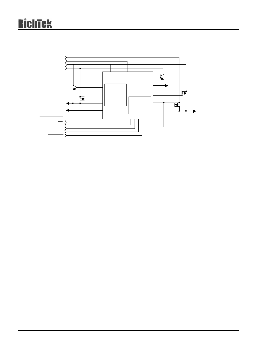
Function Block Diagram
Pin Configurations
Part Number
Pin Configurations
RT9641ACS2
(Plastic SOP-16)
RT9641BCS2
(Plastic SOP-16)
TOP VIEW
Operating temperature range
C: Commercial standard
Package type
S2 : SOP-16
V
MEM
voltage
A : 2.5V/3.3V
B : 2.6V/3.43V
MONITOR AND CONTROL
TEMPERATURE
MONITOR
(TMON)
UV
DETECTOR
_
+
1.265V
5VSB POR
TO
UV DEECTOR
EA2
TO 12V
EA4
12V BIAS
12V MONITOR
10.5V/9.5V
_
+
3.75V
_
+
40�A
0.2V
MEM VOLTAGE
SELECT COMP
UA COMPARTOR
5�A
DLA
5VDLSB
DRV2
VSEN2
GND
EN5VDL
SS
5VDL
12V
3V3DLSB
5VSB
3V3DL
EN3VDL
S3 S5
+
_
+
_
+ _
+ _
1
2
3
4
5
6
7
5VSB
EN3VDL
3V3DLSB
3V3DL
EN5VDL
S3
S5
VSEN2
DRV2
12V
SS
5VDL
5VDLSB
DLA
16
15
14
13
12
11
10
8
GND
FAULT/MSEL
9

RT9641A/B
DS9641A/B-03 March 2002
www.richtek-ic.com.tw
3
Absolute Maximum Ratings
Supply Voltage (V
5VSB
)
+7.0V
12V
GND
-0.3V to +14.5V
DLA, DRV2
GND
-0.3V to V
12V
+0.3V
All Other Pins
GND
-0.3V to 5VSB+0.3V
Package Thermal Resistance
SOP-16,
JA
100
�C/W
Maximum Junction Temperature
150
�C
Maximum Storage Temperature Range
-65
�C to 150�C
Maximum Lead Temperature (Soldering, 10 sec.)
300
�C
Recommended Operating Conditions
Supply Voltage (V
5VSB
)
+5V
� 5%
Secondary Bias Voltage (V
12V
)
+12V
� 10%
Digital Inputs (V
S3,
V
S5,
V
EN3VDL,
V
EN5VDL
)
0 to + 5.5V
Junction Temperature Range
0
�C to 125�C
Ambient Temperature Range
0
�C to 70�C
CAUTION:
Stresses beyond the ratings specified in "Absolute Maximum Ratings" may cause permanent damage to the
device. This is a stress only rating and operation of the device at these or any other conditions above those
indicated in the operational sections of this specification is not implied.
Electrical Characteristics
(V
CC
(12V
IN
)
= 12V, GND = 0V, T
A
= 25
�C, unless otherwise specified)
Parameter
Symbol
Test Conditions
Min
Typ
Max
Units
VCC Supply Current
Operating Supply Current
I
5VSB
--
7
20
mA
Shutdown Supply Current
I
5VSB(OFF)
V
SS
= 0V, S3 = 0, S5 =0
--
2
10
mA
Power-on Reset, Soft-start, and 12V Monitor
Rising 5VSB POR Threshold
--
2.5
--
V
Rising 12V Threshold
--
10.5
11
V
Soft-start Current
I
SS
--
6.5
--
�A
Shutdown Soft-start Voltage
--
0.8
--
V
To be continued
RT9641A/B
www.richtek-ic.com.tw
DS9641A/B-03 March 2002
4
Parameter
Symbol
Test Conditions
Min
Typ
Max
Units
2.5V/3.3V (2.6V/3.43V) Linear Regulator (V
OUT2
)
Regulation
--
--
2.0
%
VSEN2 Nominal Voltage Level
V
VSEN
R
SEL
= 1K
--
2.5/2.
--
V
VSEN2 Nominal Voltage Level
V
VSEN2
R
SEL
= 1K
--
3.3/3.
--
V
VSEN2 Under-voltage Falling Threshold
--
68
--
%
VSEN2 Under-voltage Hysteresis
--
7
--
%
VSEN2 Output Current
I
VSEN2
5VSB = 5V
200
300
--
mA
DRV2 Output Drive Current
I
DRV2
5VSB = 5V, R
SEL
= 1K
20
30
--
mA
DRV2 Output Impedance
R
SEL
= 10K
--
200
--
3.3V Dual Linear Regulator (V
OUT1
)
Sleep-mode Regulation
--
--
2.0
%
3V3DL Nominal Voltage Level
V
3V3DL
--
3.3
--
V
3V3DL Under-voltage Falling Threshold
--
2.24
--
V
3V3DL Under-voltage Hysteresis
--
230
--
mV
3V3DLSB Output Drive Current
I
3V3DLS
5VSB = 5V
5.0
10
--
mA
DLA Output Impedance
--
90
--
5V Dual Switch Controller (V
OUT3
)
5VDL Under-voltage Falling Threshold
--
3.40
--
V
5VDL Under-voltage Hysteresis
--
350
--
mV
5VDLSB Output Drive Current
I
5VDLSB
5VDLSB = 4V
-40
--
--
mA
Timing Intervals
Active to Sleep, Input to Switching Delay
T
d1
--
10
--
�S
Sleep to Active, Input to Switching Delay
T
d2
C
SS
= 0.1
�F
(1)
--
50
(1)
--
mS
Control I/O (S3, S5, EN3VDL, EN5VDL, FAULT)
High Level Threshold
2.0
--
--
V
Low Level Threshold
--
--
0.8
V
S3, S5 Internal Pull-up Impedance to 5VSB
--
50
--
K
FAULT Output Impedance
FAULT = high
--
100
--
Temperature Monitor
Fault-level Threshold
--
145
--
�C
Shutdown-level Threshold
T
DS
--
155
--
�C
Note:
(1)
= 50mS with 0.1
�F Soft-start capacitor. The delay time is adjustable with t
d2
= 500xC
SS
(mS).
RT9641A/B
DS9641A/B-03 March 2002
www.richtek-ic.com.tw
5
Simplified Power System Diagram
Linear
Controller
Control
Logic
RT9641A/B
Linear
Controller
Q1
V
MEM
Q4
Q5
5V
DUAL
5V
IN
12V
IN
5V
SB
3.3V
IN
Q2
Q3
3.3V
DUAL
FAULT
EN5VDL
SHUTDOWN
S3
S5
EN3VDL

RT9641A/B
www.richtek-ic.com.tw
DS9641A/B-03 March 2002
6
Functional Pin Description
5VSB (Pin 1)
Provide a 5V bias supply for the IC to this pin by
connecting it to the ATX 5VSB output. This pin also
provides the base bias current for all the external
NPN transistors controlled by the IC. The voltage at
this pin monitored for power-on reset (POR)
purposes.
EN3VDL and EN5VDL (Pin 2 and 5)
These pins control the logic governing the output
behavior in response to S3 and S4/S5 requests.
These are digital inputs whose status can only be
changed during active states operation or during chip
shutdown (SS pin grounded by external open-drain
device). The input information is latched-in when
entering a sleep state, as well as following 5VSB
POR release or exit from shutdown.
3V3DLSB (Pin 3)
Connect this pin to the base of a suitable NPN
transistor. In sleep states, this transistor is used to
regulate the voltage at 3V3DL pin to 3.3V.
3V3DL (Pin 4)
Connect this pin to the 3.3V dual output (V
OUT1
). In
sleep states, the voltage at this pin is regulated to
3.3V; in active states, ATX 3.3V output is delivered to
this node through a fully on N-MOS transistor. During
all operating states, this pin is monitored for under-
voltage events.
S3 and S5 (Pin 6 and 7)
These pins switch the IC's operating state from active
(S0, S1) to S3 and S4/S5 sleep states. Connect S3
to SLP_S3 and S5 to SLP_S5. These are digital
inputs featuring internal 50k
(typical) resistor pull-up
to 5VSB. Internal circuitry de-glitches the S3 pin for
disturbances.
GND (Pin 8)
Signal ground for the IC. All voltage levels are
measured with respect to this pin.
FAULT/MSEL (Pin 9)
This is a multiplexed function pin allowing the setting
of the memory output voltage to either 2.5V(2.6V) or
3.3V(3.43V) (for RDRAM or SDRAM memory
systems). The memory voltage setting is latched-in
when SS pin voltage goes up to 0.8V (typically 5mS
after POR). In case of an under-voltage on any of the
outputs or an over temperature event, this pin is used
to report the fault condition by being pulled to 5VSB.
DLA (Pin 10)
Connect this pin to the gates of suitable N-MOSFETs,
which in active states, are used to switch in the ATX
3.3V and 5V outputs into the 3.3V
DUAL
and 5V
DUAL
outputs, respectively.
5VDLSB (Pin 11)
Connect this pin to the gate of a suitable P-MOSFET
or bipolar PNP. In sleep states, this transistor is
switched on, connecting the ATX 5VSB output to the
5V
DUAL
regulator output. When PNP is used, it is
recommanded to use a 100
base resistor for base
current limiting.
5VDL (Pin 12)
Connect this pin to the 5V
DUAL
output (V
OUT3
). In
either operating state, the voltage at this pin is
provided through a fully on MOS transistor. This pin
is also monitored for under-voltage events.
SS (Pin 13)
Connect a small ceramic capacitor (0.1
�F
recommended) from this pin to GND. The internal
Soft-start (SS) current source along with the external
capacitor creates a voltage ramp used to control the
ramp-up of the output voltages. Pulling this pin low
with an open-drain device shuts down all the output
as well as forces the FAULT pin low. The C
SS
capacitor is also used to provide a controlled S4/S5
to active transition delay time.
RT9641A/B
DS9641A/B-03 March 2002
www.richtek-ic.com.tw
7
12V (Pin 14)
Connect this pin to the ATX (or equivalent) 12V
output. This pin is used to monitor the status of the
power supply as well as provide bias for the NMOS-
compatible output drivers. 12V presence at the chip
in the absence of bias voltage, or severe 12V
brownout during active states (S0, S1) operation can
lead to chip misbehavior. RT9641A/B refuses
entering active state before 12V power ready.
DRV2 (Pin 15)
For the 2.5V RDRAM systems, connect this pin to the
base of a suitable NPN transistor. This pass
transistor regulates the 2.5V(2.6V) output from the
ATX 3.3V during active states operation. For 3.3V
SDRAM systems connect this pin to the gate of a
suitable N-MOS transistor or the base of a suitable
NPN transistor.
VSEN2 (Pin 16)
Connect this pin to the memory output (V
OUT2
). In
sleep states, this pin is regulated to 2.5V(2.6V) or
3.3V(3.43V) (based on R
SEL
) through an internal
pass transistor capable of delivering 300mA
(Typically). The active-state voltage at this pin is
regulated through an external NPN or NMOS
transistor connected at the DRV2 pin for both
2.5V(2.6V) and 3.3V(3.43V) setting. During all
operating states, the voltage at this pin is monitored
for under-voltage events.
Description
Operation
The RT9641A/B controls 3 output voltages. It is
designed for microprocessor computer applications
with 3.3V, 5V, 5VSB, and 12V outputs from an ATX
power supply. The IC is composed of two linear
controllers supplying the PCI slots' 3.3V
AUX
power
(3.3V
DUAL
, V
OUT1
) and the 2.5V RDRAM or 3.3V
SDRAM memory power (2.5V/3.3V(2.6V/3.43V) V
MEM
,
V
OUT2
), and a dual switch controller supplying the
5V
DUAL
voltage (V
OUT3
). In addition, all the control and
monitoring functions necessary for complete ACPI
implementation are integrated into the RT9641A/B.
Initialization
The RT9641A/B automatically initializes upon receipt
of input power. The Power-On Reset (POR) function
continually monitors the 5VSB input supply voltage,
initiating soft-start operation after it exceeds its POR
threshold (in S4/S5 states). The 5VSB POR trip event
is also used to lock in the memory voltage setting
based on R
SEL
.
The RT9641A/B forces the operation mode to start
from S4/S5 states at POR releasing.
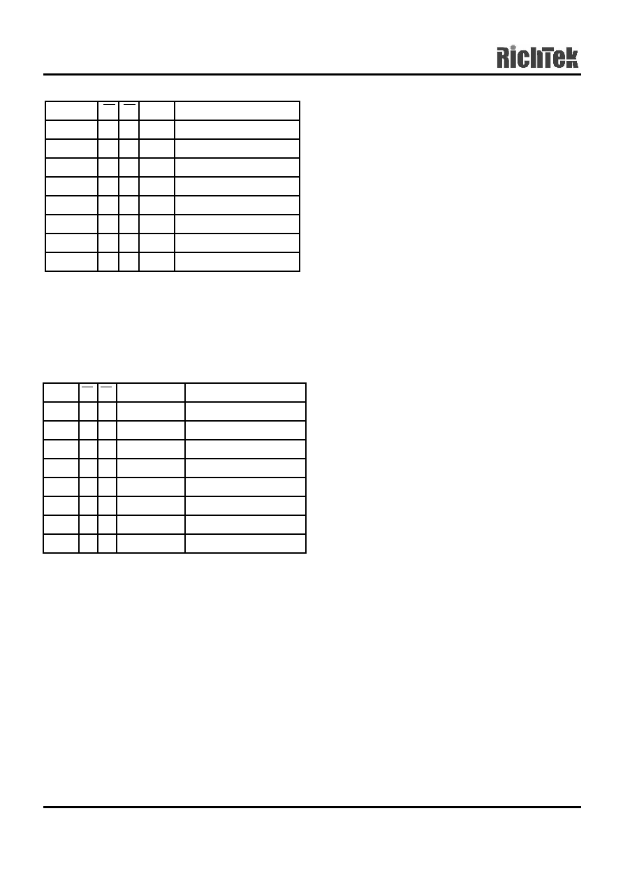
Operational Truth Tables
The EN3VDL and EN5VDL pins offer a host of choices
in terms of the overall system architecture and
supported features. Tables 1~3 describe the truth
combinations pertaining to each of the three outputs.
Table 1. 3.3V
DUAL
Output (V
OUT1
) Truth Table
EN3VDL S5 S3 3V3D
Comments
0
1
1
3.3V
S0, S1 States (Active)
0
1
0
3.3V
S3
0
0
1
Note
Maintains Previous State
0
0
0
3.3V
S4/S5
1
1
1
3.3V
S0, S1 States (Active)
1
1
0
3.3V
S3
1
0
1
Note
Maintains Previous State
1
0
0
0V
S4/S5
Note: Combination not allowed.
As seen in Table 1, EN3VDL simply controls whether
the 3.3V
DUAL
plane remains powered up during S4/S5
sleep state.
RT9641A/B
www.richtek-ic.com.tw
DS9641A/B-03 March 2002
8
Table 2. 5VDUAL Output (V
OUT3
) Truth Table
EN5VDL S5 S3 5VDL
Comments
0
1
1
5V
S0, S1 States(Active)
0
1
0
0V
S3
0
0
1
Note Maintains Previous State
0
0
0
0V
S4/S5
1
1
1
5V
S0, S1 States(Active)
1
1
0
5V
S3
1
0
1
Note Maintains Previous State
1
0
0
5V
S4/S5
Note: Combination not allowed.
Very similarly, Table 2 details the fact that EN5VDL
status controls whether the 5VDUAL plane supports
sleeps states.
Table 3. 2.5V/3.3V(2.6V/3.43V) VMEM Output (V
OUT2
)
Truth Table
RSEL S5 S3
2.5V/3.3V
Comments
1K
1
1
2.5V/2.6V
S0, S1 States(Active)
1K
1
0
2.5V
S3
1K
0
1
Note
Maintains Previous State
1K
0
0
0V
S4/S5
10K
1 1
3.3V/3.43V
S0, S1 States(Active)
10K
1 0
3.3V
S3
10K
0 1
Note
Maintains Previous State
10K
0 0
0V
S4/S5
Note: Combination not allowed.
As seen in Table 3, 2.5V/3.3V(2.6V/3.43V) VMEM
output is maintained in S3 (Suspend-To-RAM), but not
in S4/S5 state. The dual-voltage support
accommodates both SDRAM as well as RDRAM type
memories.
Fault Protection
All the outputs are monitored against under-voltage
events. A serve over-current caused by a failed load
on any of the outputs, would, in turn, cause that
specific output to suddenly drop. If any of the output
voltages drop below 68% of their set value, such event
is reported by having the FAULT/MSEL pin pulled to
5V. Additionally, the 2.5V/3.3V(2.6V/3.43V) memory
regulator is internally current limited while in a sleep
state. Exceeding the maximum current rating of this
output in a sleep state can lead to output voltage
drooping. If excessive, this droop can ultimately trip the
under-voltage detector and send a FAULT signal to the
computer system. However, a FAULT condition will
only set off the FAULT flag, and it will not shut off or
latch off any part of the circuit. If shutdown or latch off
the circuit is desired, this can be achieved by externally
pulling or latching the SS pin low. Pulling the SS pin
low will also force the FAULT pin to go low.
Under-voltage sensing is disabled on all disabled
outputs and during soft-start ramp-up intervals.
Another condition that could set off the FAULT flag is
chip over-temperature. If the RT9641A/B reaches an
internal temperature of 145
�C (typical), the FAULT flag
is set (FAULT/MSEL pulled high), but the chip
continues to operate until the temperature reaches
155
�C (typical), when unconditional shutdown of all
outputs takes place. The thermal shutdown can be
released with a re-soft-start when the chip cools down.
Shutdown
In case of a FAULT condition that might endanger the
computer system, or at any other time, the RT9641A/B
can be shut down by pulling the SS pin below the
specified shutdown level (typically 0.8V) with an open
drain or open collector device capable of sinking a
minimum of 2mA. Pulling the SS pin low effectively
shuts down all the pass elements. Upon release of the
SS pin, the RT9641A/B undergoes a new soft-start
cycle and resumes normal operation in accordance to
the ATX supply and control pins status.
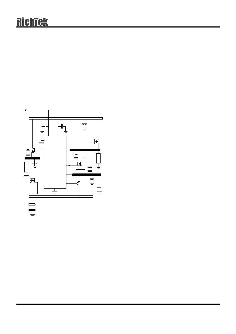
Layout Considerations
The typical application employing a RT9641A/B is a
fairly straight-forward implementation. Similar to any
other linear regulators, attention has to be paid to a
few potentially sensitive small signal components, such
as those connected to high-impedance nodes or those
supplying critical by-pass currents.
RT9641A/B
DS9641A/B-03 March 2002
www.richtek-ic.com.tw
9
The power components (pass transistors) and the
controller IC should be placed first. The controller
should be placed in a central position on the
motherboard, closer to the memory load if possible.
Ensure the VSEN2 connection is properly sized to
carry 300mA without significant resistive losses. The
pass transistors should be placed on pads capable of
heatsinking, matching the device's power dissipation.
Where applicable, multiple via corrections to a large
internal plane can significantly lower localized device
temperature rise.
Fig.1 Printed Circuit Board Islands
Placement of the decoupling and bulk capacitors
should follow a placement reflecting their purpose. As
such, the high-frequency decoupling capacitors (C
HF
)
should be placed as close as possible to the load they
are decoupling; the ones decoupling the controller
(C
12V
, C
5VSB
) close to the controller pins, the one
decoupling the load close to the load connector or the
load itself (if embedded). The bulk capacitance
(aluminum electrolytic or tantalum capacitors)
placement is not as critical as the high-frequency
capacitor placement, but having these capacitors close
to the load they serve is preferable.
The only critical small signal component is the soft-
start capacitor, C
SS
. Locate the component close to SS
pin of the control IC and connect to ground though a
vias placed close to the capacitor's ground pad.
Minimize any leakage current paths from SS node,
since the internal current source is only 5
�A.
A multi-layer printed circuit board is recommended.
Fig.1 shows the connections of most of the
components to the converter. Note that each individual
capacitor could represent numerous physical
capacitors. Dedicate one solid layer for a ground plane
and make all critical component ground connections
through vias placed as close to the component as
possible. Dedicate another solid layer as a power
plane and break this plane into smaller islands of
common voltage levels. Ideally, the power plane should
support both the input power and output power nodes.
Use copper filled polygons on the top and bottom
circuit layers to create power islands connecting the
filtering components (output capacitors) and the loads.
Use the remaining printed circuit layers for small signal
wiring.
Component Selection Guidelines
Output Capacitors Selection
The output capacitors for all outputs should be
selected to allow the output voltage to meet the
dynamic regulation requirements of active state
operation (S0, S1). The load transient for the various
microprocessor system's components may require high
quality capacitors to supply the high slew rate (di/dt)
current demands. Thus, it is recommended that
capacitors C
OUT1
and C
OUT2
should be selected for
transient load regulation.
Also, during the transition between active and sleep
states, there is a short interval of time during which
none of the power pass elements are conducting-
during this time the output capacitors have to supply all
the output current. The output voltage drop during this
brief period of time can be approximated with the
following formula:
V
OUT
= I
OUT
x (ESR
OUT
+ t
t
/ C
OUT
), where
ISLAND ON POWER PLANE LAYER
ISLAND ON CIRCUIT/POWER PLANE LAYER
VIA CONNECTION TO GROUND PLANE
LO
A
D
LO
A
D
+12V
IN
+5V
SB
C
12V
C
5VSB
C
I N
Q2
V
OUT2
+5V
IN
C
HF2
+3.3V
I N
Q1
C
BULK2
C
BULK3
C
BULK1
C
SS
V
OUT1
C
HF1
Q3
Q4
12V
5VSB
5VDLSB
5VDL
DLA
VSEN2
DRV2
GND
3V3DL
3V3DLSB
SS
V
OUT3
C
HF3
Q5
LO
A
D
RT9641A/B

RT9641A/B
www.richtek-ic.com.tw
DS9641A/B-03 March 2002
10
V
OUT
:
output voltage drop
ESR
OUT
: output capacitor bank ESR
I
OUT
: output current during transition
C
OUT
: output capacitor bank capacitance
t
t
: active-to-sleep or sleep-to-active transition time
(5
�S typical)
Since the output voltage drop is heavily dependent on
the ESR (equivalent series resistance) of the output
capacitor bank, the capacitors should be chosen to
maintain the output voltage above the lowest allowable
regulation level.
Input Capacitors Selection
The input capacitors for an RT9641A/B application
must have sufficiently low ESR so that the input
voltage does not dip excessively when energy is
transferred to the output capacitors.
Transistor Selection/Considerations
The RT9641A/B typically requires one P-channel or
PNP transistor and two N-channel power MOSFETs
and two bipolar NPN transistors.
One general requirement for selection of transistors for
all the linear regulators/switching elements is package
selection for efficient removal of heat. The power
dissipated in a linear regulator/switching element is:
P
LINEAR
= I
O
x (V
IN
� V
OUT
)
Select a package and heatsink that maintains the
junction temperature below the rating with the
maximum expected ambient temperature.
Q1
The active element on the 2.5V/3.3V (2.6V/3.43V)
V
MEM
output has different requirements for each the
two voltage settings. In 2.5V systems utilizing RDRAM
(or voltage-compatible) memory, Q1 had better to be a
bipolar NPN capable of conducting the maximum
required output current and it must have a minimum
current gain (h
fe
) of 100~150 at this current and 0.7V
V
CE
. In such systems, the 2.5V(2.6V) output is
regulated from the ATX 3.3V output while in an active
state. In 3.3V systems (SDRAM or compatible) Q1 is
suggested to use an N-channel MOSFET, then the
MOSFET serves like a switch when it is connected to
ATX3.3V during active states (S0, S1). The main
criteria for the selection of this transistor is output
voltage budgeting. The maximum R
DS(ON)
allowed at
highest junction temperature can be expressed with
the following equation:
R
DS(ON)
MAX
= (V
IN MIN
-V
OUT MIN
)/ I
OUT MAX
, where
V
IN MIN
: minimum input voltage
V
OUT
MIN
: minimum output voltage allowed.
I
OUT
MAX
: maximum output current
The gate bias available for this MOEFET is
approximately 6V, so the logic level MOSFET is
prefered. The 3.3V(3.43V) V
MEM
power also can be
regulated from ATX 5V in order to have high quality
V
MEM
, in such a configuration, either MOSFET or NPN
transistors can be used. While the heat dissipation
should be carefully handled.
Q4
If a P-chanel MOSFET is used to switch the 5VSB
output of the ATX supply into the 5V
DUAL
output during
S3 and S4/S5 states (as dictated by EN5VDL status),
then, similar to the situation where Q1 is a MOSFET,
the selection criteria of this device is also proper
voltage budgeting. The maximum r
DS (ON)
,
however,
has to be achieved with only 4.5V of V
GS
, so a logic
level MOSFET needs to be selected. If a PNP device
is chosen to perform this function, it has to have a low
saturation voltage while providing the maximum sleep-
state current and have current gain sufficiently high to
be saturated using the minimum drive current (typically
20mA). A 100~200 resistor is recommended to be
inserted between the 5VDLSB pin and Base node of
the PNP transistor for limiting the base current.
Q3, Q5
The two N-channel MOSFETs are used to switch the
3.3V and 5V inputs provided by the ATX supply into the
3.3V
DUAL
and 5V
DUAL
outputs, respectively, while in
active (S0, S1) state. Similar R
DS(ON)
criteria apply in
these cases as well, unlike the PMOS, however, these
NMOS transistors get the benefit of an increased V
GS
drive (approximately 8V and 7V respectively).
Q2
The NPN transistor used as sleep-state pass element
on the 3.3V
DUAL
output must have a minimum current
gain of 100 at V
CE
= 1.5V and I
CE
= 500mA throughout
the in-circuit operating temperature range.
RT9641A/B
DS9641A/B-03 March 2002
www.richtek-ic.com.tw
11
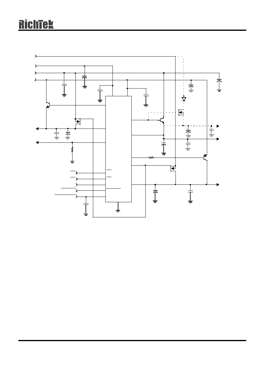
Typical Application Circuit
V
OUT2
3.3V/3.43 V
MEM
+12V
IN
+3.3V
IN
+5V
IN
+5V
SB
3V3DL
5VSB
GND
RT9641A/B
SS
C2
1
�F
C1
10
�F
C4
1
�F
Q2
2SD1802
V
OUT1
3.3V
DUAL
Q3
1/2 UF76113DK8
C6
1
�F
C7
200
�F
R1
1K
C13
0.1
�F
FAULT/MSEL
EN5VDL
(From Open-drain N-MOS)
C3
220
�F
C14
470
�F
DRV2
VSEN2
5VDLSB
100
R2
DLA
5VDL
C11
150
�F
C12
1
�F
Q5
1/2 HUF76113DK8
V
OUT3
5V
DUAL
V
OUT2
2.5V
MEM
C5
1
�F
C8,9
2X150
�F
C10
1
�F
Q1
2SD1802
Q4
MMBT2907A
3V3DLSB
12V
ER800D
CEB603AL
2X150
�F
1
�F
EN3VDL
SHUTDOWN
S3
S5
+
+
+
S3
S5
EN5VDL
EN3VDL
+
+
+
+
RT9641A/B
www.richtek-ic.com.tw
DS9641A/B-03 March 2002
12
Package Information
Dimensions In Millimeters
Dimensions In Inches
Symbol
Min
Max
Min
Max
A
9.804
10.008
0.386
0.394
B
3.810
3.988
0.150
0.157
C
1.346
1.753
0.053
0.069
D
0.330
0.508
0.013
0.020
F
1.194
1.346
0.047
0.053
H
0.178
0.254
0.007
0.010
I
0.102
0.254
0.004
0.010
J
5.791
6.198
0.228
0.244
M
0.406
1.270
0.016
0.050
M
H
B
J
A
C
I
F
D
B

RT9641A/B
DS9641A/B-03 March 2002
www.richtek-ic.com.tw
13

RT9641A/B
www.richtek-ic.com.tw
DS9641A/B-03 March 2002
14
RICHTEK TECHNOLOGY CORP.
Headquarter
6F, No. 35, Hsintai Road, Chupei City
Hsinchu, Taiwan, R.O.C.
Tel: (8863)5510047 Fax: (8863)5537749
RICHTEK TECHNOLOGY CORP.
Taipei Office (Marketing)
8F-1, No. 137, Lane 235, Paochiao Road, Hsintien City
Taipei County, Taiwan, R.O.C.
Tel: (8862)89191466 Fax: (8862)89191465
Email: marketing@richtek-ic.com.tw