128Mb: x4, x8, x16
SDRAM 3.3V
PDF: 09005aef807827f6 / Source: 09005aef807825bd
128Mb SDRAM
Rev: 11/29/2004
3
www.spectek.com
SpecTek reserves the right to change products or
specifications without notice.
©
2001, 2002, 2004 SpecTek
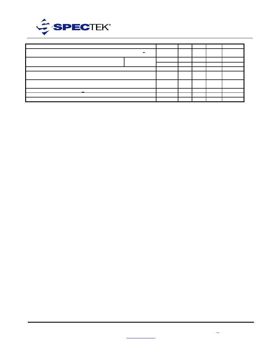
ICC OPERATING CONDITIONS AND MAXIMUM LIMITS
:
Vdd = 3.3V
±
10%V, Temp.
=
25
∞
to 70
∞
C
Supply Current
Symbol
-75A
-8A
Units
Notes
OPERATING CURRENT: ACTIVE mode, burst = 1, READ or WRITE, tRC > tRC
(MIN), one bank active, CL=3
Icc1
165
140
mA
1, 2, 3, 4
Standard parts
Idd2
9
9
mA
32
STANDBY CURRENT: POWER-DOWN mode, CKE = LOW,
no accesses in progress
Self refresh parts
Idd2
3
3
mA
32
STANDBY CURRENT: CS# = HIGH, CKE = HIGH, all banks idle
Icc3
75
60
mA
1, 2, 3, 4
STANDBY CURRENT: CS# = HIGH, CKE = HIGH, all banks active after tRCD met,
no accesses in progress.
Icc4
75
50
mA
1, 2, 3, 4
OPERATING CURRENT: BURST mode after tRCD met, continuous burst, READ,
WRITE, all banks active, CL=3
Icc5
165
145
mA
1, 2, 3, 4
AUTO REFRESH CURRENT tRC > tRC (MIN) CL = 3
Icc6
265
245
mA
1, 2, 3, 4
AUTO REFRESH CURRENT tRC=15.6us CL = 3
Icc7
50
50
mA
1, 2, 3, 4
SELF REFRESH CURRENT (Self refresh parts only, part M)
Idd8
3
3
mA
Notes
1.
All voltages referenced to Vss.
2.
An initial pause of 100
µ
s is required after power-up, followed by two AUTO REFRESH commands, before proper device operation
is ensure. (Vdd and VddQ must be powered-up simultaneously Vss and VssQ must be at the same potential.) The two AUTO
REFRESH command wake-ups should be repeated any time the
t
REF refresh requirement is exceeded.
3.
Icc specifications are tested after the device is properly initialized. tCK= 10ns for ≠8 and tCK=7.5ns for ≠75A.
128Mb: x4, x8, x16
SDRAM 3.3V
PDF: 09005aef807827f6 / Source: 09005aef807825bd
128Mb SDRAM
Rev: 11/29/2004
4
www.spectek.com
SpecTek reserves the right to change products or
specifications without notice.
©
2001, 2002, 2004 SpecTek
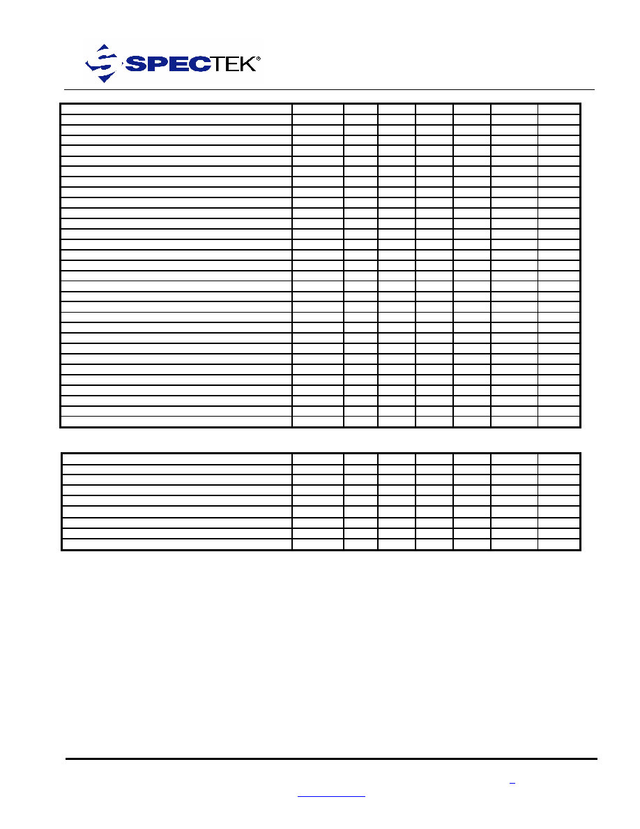
AC ELECTRICAL CHARACTERISTICS: Vdd = 3.3V
±
10%V, Temp. = 25
∞
to 70
∞
C
AC CHARACTERISTICS
-75A
-75A
-8A
-8A
PARAMETER
SYMBOL
MIN
MAX
MIN
MAX
UNITS
NOTES
Access time from CLK (positive edge) CL = 3
tAC
5.4
6
ns
Access time from CLK (positive edge) CL = 2
tAC
N/A
ns
Address hold time
tAH
0.8
1
ns
Address setup time
tAS
1.5
2
ns
CLK high level width
tCH
2.5
3
ns
CLK low level width
tCL
2.5
3
ns
Clock cycle time CL = 3
tCK
7.5
10
ns
Clock cycle time CL = 2
tCK
N/A
ns
CKE hold time
tCKH
0.8
1
ns
CKE setup time
tCKS
1.5
2
ns
CS#, RAS#, CAS#, WE#, DQM hold time
tCMH
0.8
1
ns
CS#, RAS#, CAS#, WE#, DQM setup time
tCMS
1.5
2
ns
Data-in hold time
tDH
0.8
1
ns
Data-in setup time
tDS
1.5
2
ns
Data-out high impedance time
tHZ
9
9
ns
4
Data-out low impedance time
tLZ
1
2
ns
Data-out hold time
tOH
2.7
3
ns
ACTIVE to PRECHARGE command period
tRAS
44
16K
50
16K
ns
AUTO REFRESH to ACTIVE command period
tRC
60
80
ns
ACTIVE to READ or WRITE delay
tRCD
22.5
30
ns
Refresh period (4096 cycles)
tREF
64
64
ms
PRECHARGE command period
tRP
22.5
30
ns
ACTIVE bank A to bank B command period
tRRD
15
20
ns
Transition time
tT
0.3
2
0.3
2
ns
Write recovery time
tWR
20
20
ns
3
Exit SELF REFRESH to ACTIVE command
tXSR
8
8
tCK
READ/WRITE command to READ/WRITE command
tCCD
1
1
tCK
1
CKE to clock disable or power down entry mode
tCKED
1
1
tCK
2
CKE to clock enable or power down exit setup
tPED
1
1
tCK
2
AC ELECTRICAL CHARACTERISTICS: Vdd = 3.3V
±
10%V, Temp. = 25
∞
to 70
∞
C
AC CHARACTERISTICS
-75A
-75A
-8
-8
PARAMETER
SYMBOL
MIN
MAX
MIN
MAX
UNITS
NOTES
DQM to input data delay
tDQD
0
0
tCK
1
WRITE command to input data delay
tDWD
0
0
tCK
1
Data-in to ACTIVATE command w/ Auto precharge
tDAL
5
5
tCK
3
Data-in to precharge
tDPL
2
2
tCK
2, 3
Last data-in to precharge command
tRDL
2
2
tCK
1
LOAD MODE REGISTER command to command
tMRD
2
2
tCK
1
Data-out to high impedance from precharge
tROH
3
3
tCK
1
NOTES:
1.
Clocks required specified by JEDEC functionality and not dependent on any timing parameter.
2.
Timing actually specified by tCKS, clock(s) specified as a reference only at a minimum cycle rate.
3.
Timing actually specified by tWR plus tRP clock(s) specified as a reference only at a minimum cycle rate.
4.
tHZ defines the time at which the output achieves the open circuit condition; it is not a reference to Voh or Vol. The last valid data
element will meet tOH before going high-Z.
5.
Based on tCK = 10ns for ≠8 and tCK = 7.5ns for ≠75a
128Mb: x4, x8, x16
SDRAM 3.3V
PDF: 09005aef807827f6 / Source: 09005aef807825bd
128Mb SDRAM
Rev: 11/29/2004
5
www.spectek.com
SpecTek reserves the right to change products or
specifications without notice.
©
2001, 2002, 2004 SpecTek
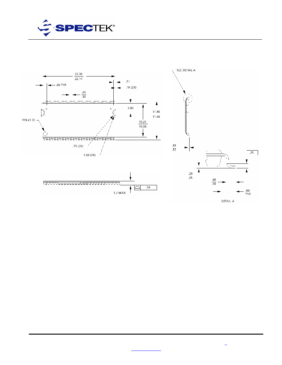
54-PIN PLASTIC TSOP (400 mil)
(Package TK)
NOTE: 1. All dimensions in millimeters MAX/MIN or typical where noted.
2. Package width and length do not include mold protrusion; allowable mold protrusion is 0.25mm per side.