SUMMIT MICROELECTRONICS, Inc. ∑ 300 Orchard City Drive, Suite 131 ∑ Campbell, CA 95008 ∑ Telephone 408-378-6461 ∑ Fax 408-378-6586 ∑ www.summitmicro.com
1
© SUMMIT MICROELECTRONICS, Inc. 1998
2008 1.4 5/15/98
Characteristics subject to change without notice
SUMMIT
MICROELECTRONICS, Inc.
FEATURES
∑
Voltage ProtectionTM
∑
Precision Low-V
CC
Write Lockout
∑
All Write Operations Inhibited When V
CC
Falls
below V
LOCK
∑
One 3Volt and Two 5Volt System Versions
≠ V
LOCK
= 2.6V+.1V/-.05V
≠ V
LOCK
= 4.25V +.25V/-0.0V
≠ V
LOCK
= 4.50 +.25V/-0.0V
∑
100% Compatible with Industry Standard I
2
CTM
Devices
≠ Bi-directional data transfer protocol
≠ Standard 100kHz and 400kHz Transfer Rates
∑
16-Byte Page-Write Mode
≠ Minimizes total write time per byte
∑
1,000,000 Program/Erase Cycles
∑
100 Year Data Retention
∑
Commercial Industrial Temperature Range
4K Serial E
2
PROM with a Precision Low-V
CC
Lockout Circuit
S24VP04
OVERVIEW
The S24VP04 is a 4K-bit serial E
2
PROM memory inte-
grated with a precision V
CC
sense circuit. The sense
circuit will disable write operations whenever V
CC
falls
below the V
LOCK
voltage. It is fabricated using SUMMIT's
advanced CMOS E
2
PROM technology and is suitable for
both 3 and 5 volt systems.
The S24VP04 is internally organized as 512 x 8. It fea-
tures the I
2
C serial interface and software protocol allow-
ing operation on a simple two-wire bus.
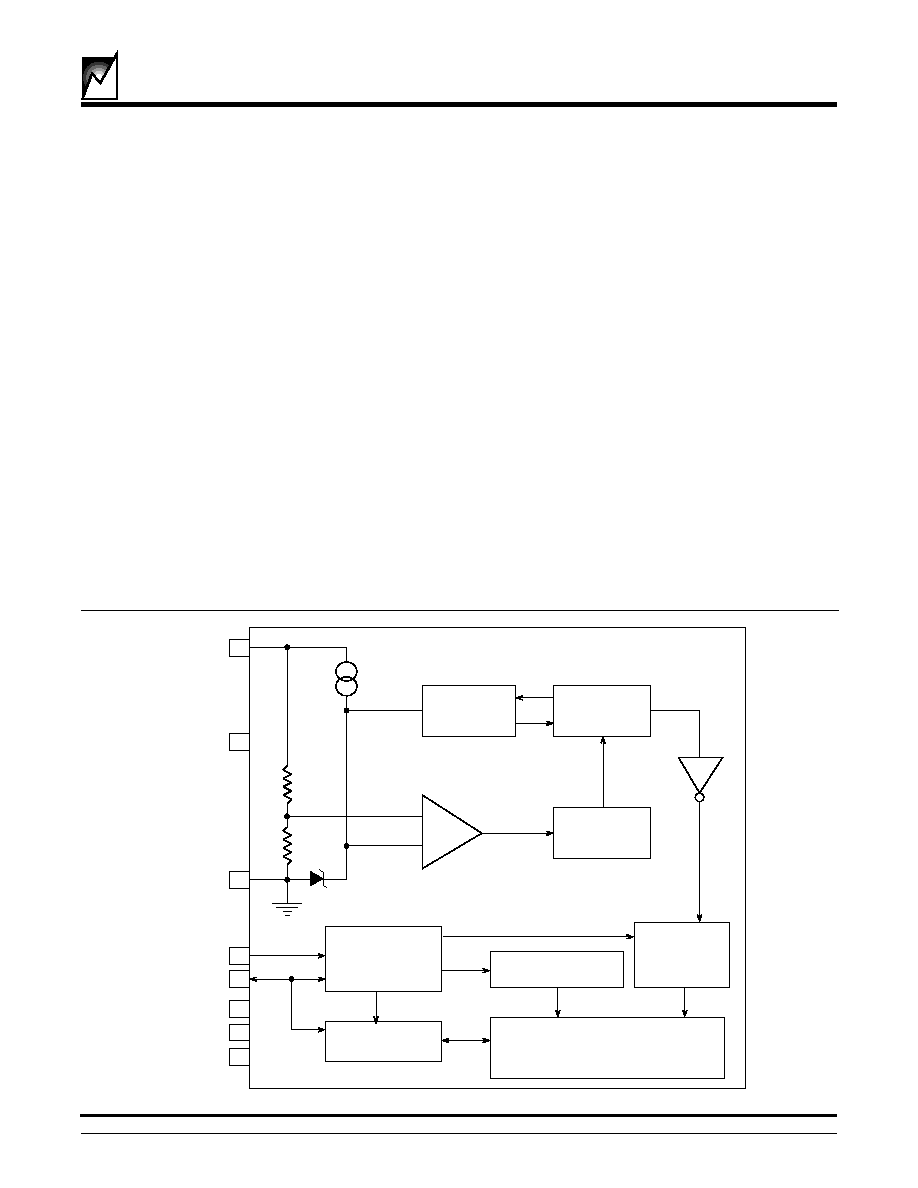
BLOCK DIAGRAM
3 and 5 Volt Systems
+
-
7
2
VCC
8
NC
SDA
NC
SCL
1
6
3
4
5
GND
NC
NC
2008 ILL2 1.2
E2PROM
MEMORY
ARRAY
ADDRESS
DECODER
WRITE
CONTROL
RESET
CONTROL
RESET
PULSE
GENERATOR
5KHz
Oscillator
VTRIP
1.26V
MODE
DECODE
DATA I/O

2
S24VP04
2008 1.4 5/15/98
Address Inputs A0, A1, A2- Device Address Inputs
These inputs are unused by the S24VP04; however, to
ensure proper operation they should be left unconnected
or tied to ground. The should not be tied high.
ENDURANCE AND DATA RETENTION
The S24VP04 is designed for applications requiring
1,000,000 erase/write cycles and unlimited read cycles. It
provides 100 years of secure data retention, with or
without power applied, after the execution of 1,000,000
erase/write cycles.
DEVICE OPERATION
APPLICATIONS
The S24VP04 was designed specifically for applications
where the integrity of the stored data is paramount. In
recent years, as the operating voltage range of serial
E
2
PROMs has widened, most semiconductor manufac-
turers have arbitrarily eliminated their V
CC
sense circuits.
The S24VP04 will protect your data by guaranteeing write
lockout below the selected V
CC
Lockout voltage.
V
CC
Lockout
The S24VP04 has an on-board precision V
CC
sense
circuit. Whenever V
CC
is below V
LOCK
, the S24VP04 will
disable the internal write circuitry. The V
CC
lockout circuit
will ensure a higher level of data integrity than can be
expected from industry standard devices that have either
a very loose specification or no V
CC
lockout specification.
During a power-on sequence all writes will be inhibited
below the V
LOCK
level and will continue to be held in a write
inhibit state for approximately 200ms after V
CC
reaches,
then stays at or above V
LOCK
. The 200ms delay provides
a buffer space for the microcontroller to complete its
power-on initialization routines (reading is OK) while still
protecting against inadvertent writes.
During a power-down sequence initiation of writes will be
inhibited whenever V
CC
falls below V
LOCK
. This will guard
against the system's microcontroller performing an inad-
vertent write within the `danger zone'. (see AN001)
PIN DESCRIPTIONS
Serial Clock (SCL) - The SCL input is used to clock data
into and out of the device. In the WRITE mode, data must
remain stable while SCL is HIGH. In the READ mode, data
is clocked out on the falling edge of SCL.
Serial Data (SDA) - The SDA pin is a bidirectional pin
used to transfer data into and out of the device. Data may
change only when SCL is LOW, except START and STOP
conditions. It is an open-drain output and may be wire-
ORed with any number of open-drain or open-collector
outputs.
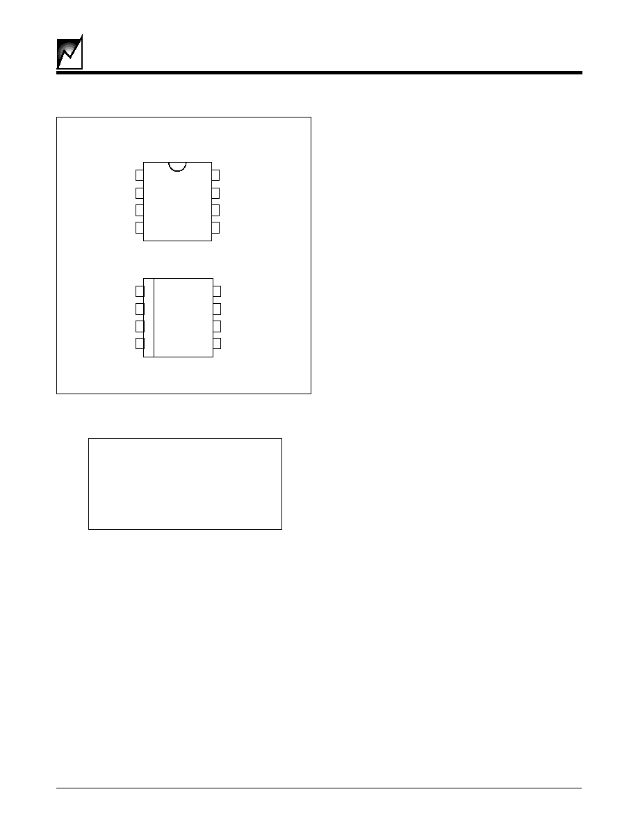
PIN NAMES
A0, A1,A2
Address Inputs
SDA
Serial Data I/O
SCL
Serial Clock Input
DC
Don't Care
GND
Ground
V
CC
Supply Voltage
PIN CONFIGURATIONS
8
7
6
5
1
2
3
4
A0
A1
A2
GND
V
CC
DC
SCL
SDA
A0
A1
A2
GND
V
CC
DC
SCL
SDA
Plastic Dual-in-line
"P" Package
8
7
6
5
1
2
3
4
JEDEC Small Outline
"S" Package
2008 ILL1 1.2

S24VP04
3
2008 1.4 5/15/98
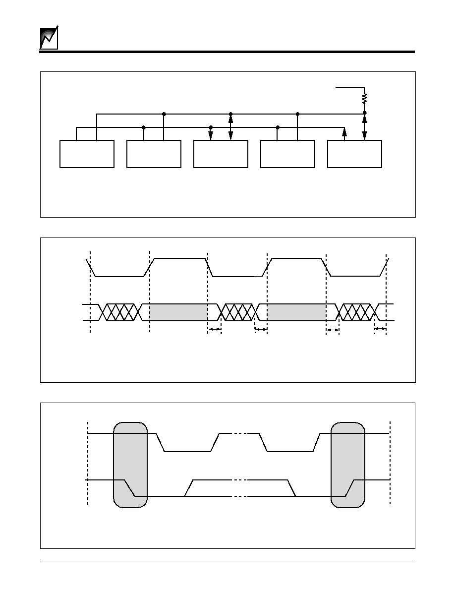
FIGURE 1. TYPICAL SYSTEM CONFIGURATION
FIGURE 3. START AND STOP CONDITIONS
FIGURE 2. INPUT DATA PROTOCOL
Data must
remain stable
while clock
is HIGH.
Data must
remain stable
while clock
is HIGH.
Change
of data
allowed
SCL
SDA In
t
HD:DAT
t
SU:DAT
t
HD:DAT
2008 ILL4 1.0
SCL
SDA In
START
Condition
STOP
Condition
2008 ILL5 1.0
Master
Transmitter
SDA
SCL
Slave
Transmitter/
Receiver
Master
Transmitter/
Receiver
Slave
Receiver
Master
Transmitter/
Receiver
Vcc
(
µ
C/
µ
P)
(24VP04)
2008 ILL 3 1.1
RESET

4
S24VP04
2008 1.4 5/15/98
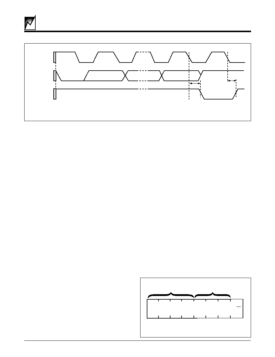
FIGURE 4. ACKNOWLEDGE RESPONSE FROM RECEIVER
CHARACTERISTICS OF THE I
2
C BUS
General Description
The I
2
C bus was designed for two-way, two-line serial
communication between different integrated circuits. The
two lines are: a serial data line (SDA), and a serial clock
line (SCL). The SDA line must be connected to a positive
supply by a pull-up resistor, located somewhere on the
bus (See Figure 1). Data transfer between devices may
be initiated with a START condition only when SCL and
SDA are HIGH (bus is not busy).
Input Data Protocol
One data bit is transferred during each clock pulse. The
data on the SDA line must remain stable during clock
HIGH time, because changes on the data line while SCL
is HIGH will be interpreted as start or stop condition (See
Figure 2).
START and STOP Conditions
When both the data and clock lines are HIGH, the bus is
said to be not busy. A HIGH-to-LOW transition on the data
line, while the clock is HIGH, is defined as the "START"
condition. A LOW-to-HIGH transition on the data line,
while the clock is HIGH, is defined as the "STOP" condi-
tion (See Figure 3).
DEVICE OPERATION
The S24VP04 is a 16,384-bit serial E
2
PROM. The device
supports the I
2
C bidirectional data transmission protocol.
The protocol defines any device that sends data onto the
bus as a "transmitter" and any device which receives data
as a "receiver." The device controlling data transmission
is called the "master" and the controlled device is called
the "slave." In all cases, the S24VP04 will be a "slave"
device, since it never initiates any data transfers.
FIGURE 5. SLAVE ADDRESS BYTE
Acknowledge (ACK)
Acknowledge is a software convention used to indicate
successful data transfers. The transmitting device, either
the master or the slave, will release the bus after transmit-
ting eight bits. During the ninth clock cycle, the receiver
will pull the SDA line LOW to ACKnowledge that it re-
ceived the eight bits of data (See Figure 4).
The S24VP04 will respond with an ACKnowledge after
recognition of a START condition and its slave address
byte. If both the device and a write operation are selected,
the S24VP04 will respond with an ACKnowledge after the
receipt of each subsequent 8-bit word.
In the READ mode, the S24VP04 transmits eight bits of
data, then releases the SDA line, and monitors the line for
an ACKnowledge signal. If an ACKnowledge is detected,
and no STOP condition is generated by the master, the
S24VP04 will continue to transmit data. If an ACKnowledge
is not detected, the S24VP04 will terminate further data
transmissions and awaits a STOP condition before return-
ing to the standby power mode.
Device Addressing
Following a start condition the master must output the
address of the slave it is accessing. The most significant
four bits of the slave address are the device type identifier
(see figure 5). For the S24VP04 this is fixed as 1010[B].
SCL from
Master
Data Output
from
Transmitter
Data Output
from
Receiver
Start
Condition
ACKnowledge
t
AA
t
AA
1
8
9
2008 ILL6 1.0
1 0 1 0
S2 S1 BS
DEVICE
IDENTIFIER
HIGH ORDER
WORD ADDRESS
2008 ILL7 1.0
(A8)

S24VP04
5
2008 1.4 5/15/98
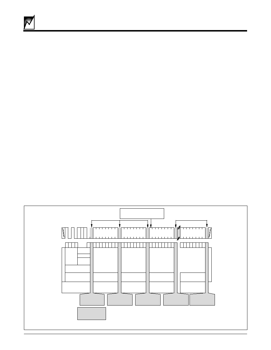
FIGURE 6. PAGE/BYTE WRITE MODE
WRITE OPERATIONS
The S24VP04 allows two types of write operations: byte
write and page write. The byte write operation writes a
single byte during the nonvolatile write period (t
WR
). The
page write operation allows up to 16 bytes in the same
page to be written during t
WR
.
Byte WRITE
After the slave address is sent (to identify the slave
device, specify high order word address and a read or
write operation), a second byte is transmitted which
contains the low 8 bit addresses of any one of the 512
words in the array.
Upon receipt of the word address, the S24VP04 responds
with an ACKnowledge. After receiving the next byte of
data, it again responds with an ACKnowledge. The mas-
ter then terminates the transfer by generating a STOP
condition, at which time the S24VP04 begins the internal
write cycle.
While the internal write cycle is in progress, the S24VP04
inputs are disabled, and the device will not respond to any
requests from the master. Refer to Figure 6 for the
address, ACKnowledge and data transfer sequence.
Page WRITE
The S24VP04 is capable of a 16-byte page write opera-
tion. It is initiated in the same manner as the byte-write
operation, but instead of terminating the write cycle after
the first data word, the master can transmit up to 15 more
words of data. After the receipt of each word, the
S24VP04 will respond with an ACKnowledge.
The S24VP04 automatically increments the address for
subsequent data words. After the receipt of each word,
the four low order address bits are internally incremented
by one. The high order five bits of the address byte remain
constant. Should the master transmit more than sixteen
words, prior to generating the STOP condition, the ad-
dress counter will "roll over," and the previously written
data will be overwritten. As with the byte-write operation,
all inputs are disabled during the internal write cycle.
Refer to Figure 6 for the address, ACKnowledge and data
transfer sequence.
The next two bits are don't care. The S24VP04 will
respond to all commands for device 1010.
Bank Select Bit
The next bit of the serial stream is the bank select bit. It is
used by the host to toggle between the two 2K-bit banks
of memory. It is, in effect, the most significant bit of the
word address, or A8.
Read/Write Bit
The last bit of the data stream defines the operation to be
performed. When set to "1," a read operation is selected;
when set to "0," a write operation is selected.
D
7
D
6
D
5
D
4
D
3
D
2
D
1
D
0
D
7
D
6
D
5
D
4
D
3
D
2
D
1
D
0
A
7
A
6
A
5
A
4
A
3
A
2
A
1
A
0
D
7
D
5
D
6
D
4
D
0
D
3
D
2
D
1
S
T
A
R
T
Word Address
Data Byte n
Data Byte n+15
S
T
O
P
A
C
K
Acknowledges Transmitted from
24VP04 to Master Receiver
Slave Address
Device
Type
Address
Read/Write
0= Write
A2,A1,BS
SDA
Bus
Activity
A
C
K
A
C
K
Master Sends Read
Request to Slave
Master Writes Word
Address to Slave
1 0 1 0
0
Data Byte n+1
A
C
K
Master Writes
Data to Slave
Master Transmitter
to
Slave Receiver
Slave Transmitter
to
Master Receiver
Slave Transmitter
to
Master Receiver
Master Transmitter
to
Slave Receiver
Master Transmitter
to
Slave Receiver
Shading Denotes
24VP04
SDA Output Active
Master Transmitter
to
Slave Receiver
Slave Transmitter
to
Master Receiver
Slave Transmitter
to
Master Receiver
Master Transmitter
to
Slave Receiver
Slave Transmitter
to
Master Receiver
Master Writes
Data to Slave
Master Writes
Data to Slave
Acknowledges Transmitted from
24043 to Master Receiver
If single byte-write only,
Stop bit issued here.
A
2
A
1
R
W
A
C
K
B
S
2008 ILL8 1.0
