This Datasheet states Saifun's current technical specifications regarding the Products described herein. This Datasheet
may be revised by subsequent versions or modifications due to changes in technical specifications.
Publication# 1908 Rev: 1 Amendment: 1
Issue Date: 26 August 2003
SA24C1024
Datasheet
Features
∑
=
Saifun NROMTM NVM Technology
∑
=
Operating voltage: 2.7V to 3.6V
∑
=
Clock frequency: 100/400/1700/3400 kHz
∑
=
Low power consumption
≠
0.5
µ
µ
µ
µ
A standby current typical (L version)
≠
<0.2
µ
µ
µ
µ
A standby current typical (LZ version)
∑
=
Write Modes
≠
Byte Mode
≠
Page Mode (128 Bytes/Page)
∑
=
Schmitt trigger inputs
∑
=
Hardware and software write protection for entire or partial array
∑
=
Endurance: up to 1 million data changes
∑
=
Data Retention: Greater than 40 years
∑
=
Packages: 8-Pin DIP and 8-Pin SOIC and MLF Leadless
∑
=
Temperature range
≠
Commercial: 0 ∞C to +70 ∞C
≠
Industrial (E): -40 ∞C to +85 ∞C
1024Kb EEPROM
IIC
http://www.saifun.com
Saifun NROM
TM
is a trademark of Saifun Semiconductors Ltd.

SA24C1024 Datasheet
SAIFUN
3
Table of Contents
Features ......................................................................... 1
General Description ...................................................... 2
Block Diagram ............................................................... 4
Connection Diagrams ................................................... 5
Ordering Information .................................................... 6
Product Specifications ................................................. 7
Absolute Maximum Ratings Operating Conditions... 7
ESD/Latch up Specification (JEDEC 8 Spec) ........... 7
Operating Conditions............................................... 7
V
CC
(2.7 V to 3.6 V) DC Electrical Characteristics ... 8
Capacitance ............................................................ 8
AC Test Conditions ................................................. 9
AC Testing Input/Output Waveforms....................... 9
AC Characteristics (V
CC
2.7 V ≠ 3.6 V).................... 9
Bus Timing ............................................................ 10
Write Cycle Timing ................................................ 11
Typical System Configuration................................ 11
Background Information (IIC Bus) ............................. 12
Slave Address ....................................................... 12
Device Type .......................................................... 13
Device/Page Block Selection................................. 13
Read/Write Bit....................................................... 13
Acknowledge......................................................... 13
Array Address#1.................................................... 13
Array Address#0.................................................... 13
Pin Descriptions.......................................................... 14
Serial Clock (SCL)................................................. 14
Serial Data (SDA).................................................. 14
Write Protect (WP) ................................................ 14
Choice 1: Full Array Write Protect ................. 14
Device Selection Input ≠ A1 (as Appropriate) ........ 14
Choice 2: Programmable Write Protect
......... 15
Device Operation......................................................... 16
Clock and Data Conventions ................................. 16
START Condition .................................................. 16
STOP Condition .................................................... 16
SA24C1024 Array Addressing............................... 16
Write Operations ......................................................... 18
Byte Write ............................................................. 18
Page Write ............................................................ 18
Acknowledge Polling ............................................. 19
Write Protection .................................................... 19
Read Operations ......................................................... 20
Current Address Read........................................... 20
Random Read ....................................................... 20
Sequential Read.................................................... 20
Switching from Standard/Fast Modes to High-speed
Mode and Back ....................................................... 22
Physical Dimensions................................................... 24
Contact Information .................................................... 27
Life Support Policy...................................................... 27
List of Figures
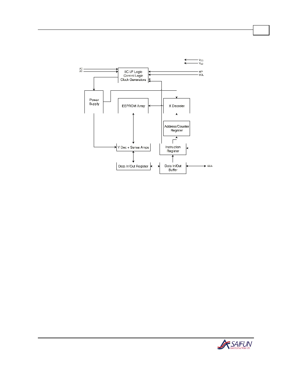
Figure 1. SA24C1024 Block Diagram.............................. 4
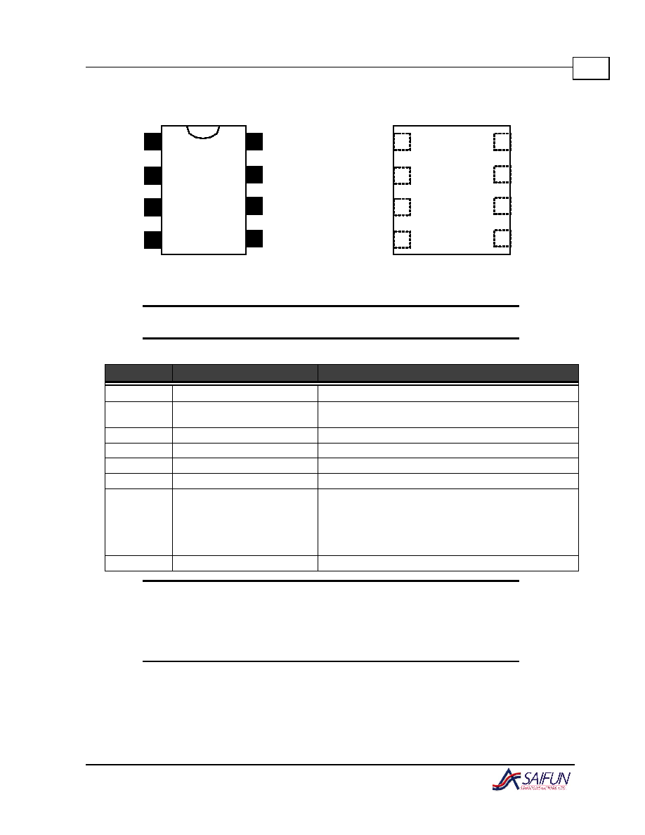
Figure 2. SO Package (MW), Dual Inline (N) ≠ Top View 5
Figure 3. Leadless Package (MLF) ≠ Top View ............... 5
Figure 4. SA24C1024 Ordering Information..................... 6
Figure 5. AC Testing Input/Output Waveforms ................ 9
Figure 6. Bus Timing ..................................................... 10
Figure 7. Write Cycle Timing ......................................... 11
Figure 8. Typical System Configuration......................... 11
Figure 9. Slave Address ................................................ 12
Figure 10. Data Validity ................................................. 17
Figure 11. START and STOP Definition ........................ 17
Figure 12. Acknowledge Response from Receiver ........ 17
Figure 13. Byte Write .................................................... 19
Figure 14. Page Write ................................................... 19
Figure 15. Current Address Read.................................. 21
Figure 16. Random Read .............................................. 21
Figure 17. Sequential Read........................................... 21
Figure 18. Data Transfer ............................................... 22
Figure 19. A Complete HS Mode Transfer..................... 23
Figure 20. 8-pin Molded Small Outline Package (MW8),
Package Number M08D ...................................... 24
Figure 21. Molded Dual-in-Line Package (N), Package
Number N08E...................................................... 25
Figure 22. 8-pin MLF Leadless Package ....................... 26
List of Tables
Table 1. Pin Names......................................................... 5
Table 2. Write Protection Truth Table............................ 14