 | –≠–ª–µ–∫—Ç—Ä–æ–Ω–Ω—ã–π –∫–æ–º–ø–æ–Ω–µ–Ω—Ç: SED1190 | –°–∫–∞—á–∞—Ç—å:  PDF PDF  ZIP ZIP |
705
SED1190
CMOS LCD 64-COMMON DRIVERS
s
DESCRIPTION
The SED1190 is a dot matrix LCD common (row) driver for driving high-capacity LCD panel at duty cycles
higher than 1/64. The LSI uses two serially connected, 32-bit shift registers to hold the display data, and level
shifter converts the TTL level 64-bit parallel data from the shift registers to levels suitable for use by the LCD
drive circuitry. The SED1190 generates common drive signals using the voltages supplied to LCD drive
voltages pins.
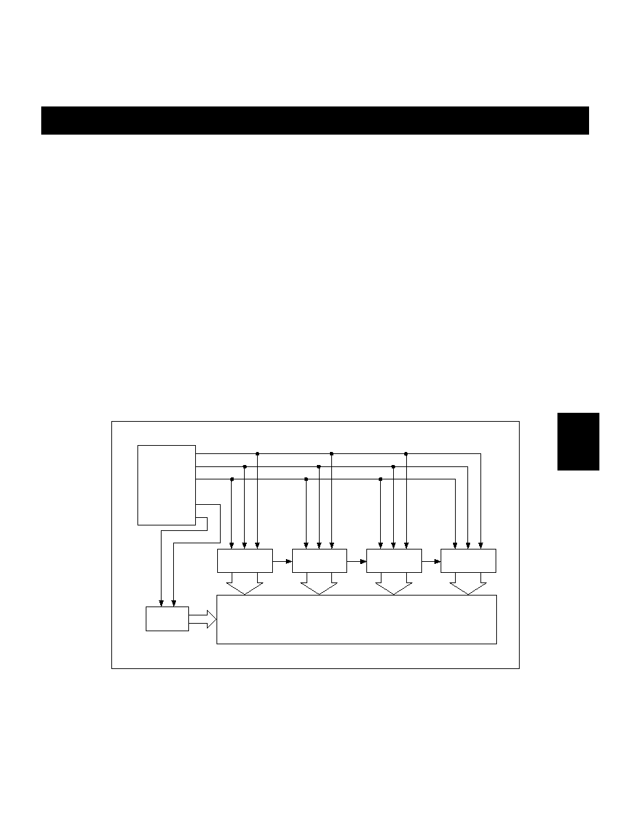
The SED1190 is used in conjunction with the SED1180 (64-bit row driver) to drive a large capacity dot matrix
LCD panel.
s
FEATURES
∑
Low-power CMOS technology
∑
64-bit common (row) driver
∑
Display blanking
∑
Duty cycle: 1/64 to 1/128
∑
Daisy chain enable support
∑
Wide range of LCD voltage: ≠14V to ≠25V
∑
Supply voltage: 5.0V
±
10%
∑
Package: ............................... QFP1-80 pin (F
0A
)
QFP5-80 pin (F
5A
)
DIE: Al pad chip (D
0A
)
s
SYSTEM BLOCK DIAGRAM
SED1180F
SED1180
SED1180
SED1180
LCD
CONTR
256SEG
◊
64 COM
DUTY: 1/64
SED1190
64
64
64
64
64
D0 ~ D3
XSCL
YSCL
YD
LP, FR
706
s
BLOCK DIAGRAM
LCD Driver
Level Shifter
Shift Register
32 bits
32 bits
32 bits
Shift Register
Level Shifter
LCD Driver
32 bits
32 bits
32 bits
Voltage Control
Latch
0
31
32
63
5
COM
COM
DI
INH
YSCL
FR
V
SS
V
DD
V2
V3
V
SSH
DO
LAT
SED1190
s
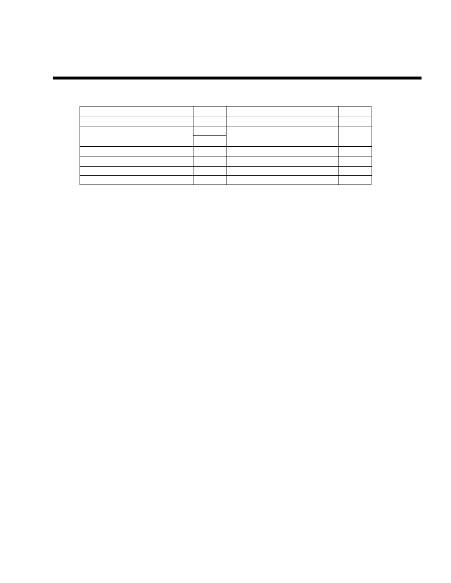
PIN CONFIGURATION
Index
5
1
10
15
20
25
30
35
45
50
55
60
65
70
75
80
SED1190
DO
V
SSH
V
4
NC
NC
NC
NC
V
1
V
SS
V
DD
NC
DI
LAT
INH
FR
YSCL
COM39
COM38
COM37
COM36
COM35
COM34
COM33
COM32
COM0
COM1
COM2
COM3
COM4
COM5
COM6
COM7
COM63
COM62
COM61
COM60
COM59
COM58
COM57
COM56
COM55
COM54
COM53
COM52
COM51
COM50
COM49
COM48
COM47
COM46
COM45
COM44
COM43
COM42
COM41
COM40
COM31
COM30
COM29
COM28
COM27
COM26
COM25
COM24
COM23
COM22
COM21
COM20
COM19
COM18
COM17
COM16
COM15
COM14
COM13
COM12
COM11
COM10
COM9
COM8
40

707
SED1190
Number
Name
Number
Name
Number
Name
Number
Name
1
COM31
21
COM11
41
COM40
61
COM60
2
COM30
22
COM10
42
COM41
62
COM61
3
COM29
23
COM 9
43
COM42
63
COM62
4
COM28
24
COM 8
44
COM43
64
COM63
5
COM27
25
COM 7
45
COM44
65
DO
6
COM26
26
COM 6
46
COM45
66
V
SSH
7
COM25
27
COM 5
47
COM46
67
V4
8
COM24
28
COM 4
48
COM47
68
NC
9
COM23
29
COM 3
49
COM48
69
NC
10
COM22
30
COM 2
50
COM49
70
NC
11
COM21
31
COM 1
51
COM50
71
NC
12
COM20
32
COM 0
52
COM51
72
V1
13
COM19
33
COM32
53
COM52
73
V
SS
14
COM18
34
COM33
54
COM53
74
V
DD
15
COM17
35
COM34
55
COM54
75
NC
16
COM16
36
COM35
56
COM55
76
DI
17
COM15
37
COM36
57
COM56
77
LAT
18
COM14
38
COM37
58
COM57
78
INH
19
COM13
39
COM38
59
COM58
79
FR
20
COM12
40
COM39
60
COM59
80
YSCL
NC = Not connected
Pin Name
Function
COM0 to COM63
LCD common drive outputs
DI
Serial data input
Transparent latch control input:
LAT
DI
DI latch output
LAT
H
H
H
L
L
L
X
DI latch
DO
Serial data output
YSCL
Serial data shift clock. Data is shifted through the controller on the falling
edge of this clock
FR
LCD AC-drive signal input
INH
Active-low blanking input
V
DD
, V
SS
Logic power supply inputs
V1, V4, V
SSH
LCD drive power inputs
V
DD
V1
V4
V
SSH
s
PIN DESCRIPTION
708
SED1190
s
ELECTRICAL CHARACTERISTICS
∑
Absolute Maximum Ratings
Parameter
Symbol
Ratings
Unit
Supply voltage (1)
V
SS
≠7.0 to +0.3
V
Supply voltage (2)
V
SSH
≠28.0 to +0.3
V
V1, V4
Input voltage
V
I
V
SS
≠0.3 to +0.3
V
Operating temperature
T
opr
≠20 to +75
∞
C
Storage temperature
T
stg
≠55 to +125
∞
C
Soldering temperature and time
T
sol
260, 10
∞
C, s
Notes:
1. All voltages referenced to a V
DD
of 0 V.
2. V1 and V4 must satisfy the relationship V
DD
V1, V4
V
SSH
3. Exceeding the absolute maximum ratings can cause permanent damage to the device. Functional operation under these
conditions is not implied.
4. Moisture resistance of flat packages can be reduced by the soldering process. Care should be taken to avoid thermally
stressing the package during board assembly.
709
∑
DC Characteristics
Parameter
Symbol
Conditions
Rating
Unit
Min
Typ
Max
Supply voltage (1)
V
SS
≠5.5
≠5.0
≠4.5
V
V1
V
SSH
--
V
DD
V
Supply voltage (2)
V4
V
SSH
--
V
DD
V
V
SSH
Recommended V
SSH
≠25.0
--
≠14.0
V
Operable V
SSH
(see note)
≠25.0
--
≠5.0
V
High level input voltage
V
IH
0.2V
SS
--
V
DD
+0.3
V
Low level input voltage
V
IL
V
SS
≠0.3
--
0.8V
SS
V
High level output voltage
V
OH
I
OH
= ≠0.6 mA
≠0.4
--
--
V
Low level output voltage
V
OL
I
OL
= 0.6 mA
--
--
V
SS
+0.4
V
Input leakage current
I
LI
0 V
V
I
V
SS
--
0.05
2.0
µ
A
Output leakage current
I
LO
0 V
V
O
V
SS
--
0.05
5.0
µ
A
Shift clock
YSCL
--
--
2.5
MHz
Frame signal
FR
--
1/60
--
s
Input capacitance
C
I
T
a
= 25
∞
C
--
5.0
8.0
pF
V
SSH
= ≠20.0 V
--
0.8
1.0
Common output on
R
COM
V
SSH
= ≠14.0 V
--
0.9
1.3
k
resistance
V
SSH
= ≠9.0 V
--
1.3
2.0
V
SSH
= ≠5.0 V
--
3.0
30.0
Quiescent current
I
Q
SED
V
SSH
= ≠25 V, V
SSH
= ≠5.5 V,
--
0.05
30
µ
A
1190
V
I
= V
DD
V
SS
= ≠5.0 V,
V
IH
= V
DD
,
V
IL
= V
SS
,
YSCL cycle =
Operating current for
I
SS
FR cycle = 16.7 ms
130
µ
s
--
3.0
8.0
µ
A
the logic
(duty 50%), All
"H" output
terminals are
opened at every
data input all
1/128 duty.
V
SS
= ≠4.5 V,
V
1
= ≠2.0 V,
V
4
= ≠18.0 V,
YSCL cycle =
Operating current for LCD
I
SSH
FR cycle = 16.7 ms
130
µ
s
--
3.0
8.0
µ
A
(duty 50%), All
"H" output
terminals are
opened at every
data input of
1/128 duty.
Pull up MOS current
≠I
p
V
SS
= ≠5.0 V, V
IL
= ≠5.0 V
10.0
25.0
50.0
µ
A
Applicable to LAT input terminals
V
OH
= V
DD
≠0.5 V
V
OL
= V
SSH
+0.5 V
COM bit
(V
DD
= 0V, V
SS
= ≠5.0 V
±
10%, T
a
= ≠20 to 75
∞
C)
Note: Error free operation is guaranteed in this range but the output resistance of the LCD drivers is higher than in the recommended
operating range. It is suggested that the driver is tested with the target LCD panel to determine if performance is acceptable.
SED1190