 | ÐлекÑÑоннÑй компоненÑ: SED1336F | СкаÑаÑÑ:  PDF PDF  ZIP ZIP |
Äîêóìåíòàöèÿ è îïèñàíèÿ www.docs.chipfind.ru

S-MOS Systems, Inc. · 2460 North First Street · San Jose, CA 95131 · Tel: (408) 922-0200 · Fax: (408) 922-0238
268-0.4
1
SED1330F/1335F/1336F
LCD Controller ICs
Technical Manual
S-MOS Systems, Inc.
September, 1995
Version 0.4

S-MOS Systems, Inc. · 2460 North First Street · San Jose, CA 95131 · Tel: (408) 922-0200 · Fax: (408) 922-0238
2
268-0.4
THIS PAGE INTENTIONALLY BLANK

S-MOS Systems, Inc. · 2460 North First Street · San Jose, CA 95131 · Tel: (408) 922-0200 · Fax: (408) 922-0238
268-0.4
3
Table of Contents
SED1330F/1335F/1336F
CONTENTS
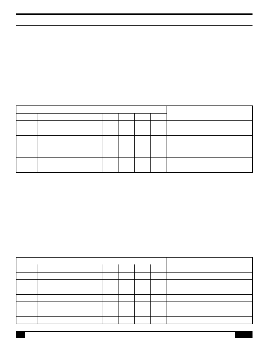
1.0 Overview ............................................................................................................. 9
1.1 Description .................................................................................................................................. 11
1.2 Features ...................................................................................................................................... 11
1.3 Block Diagram ............................................................................................................................. 12
1.4 Pinouts ........................................................................................................................................ 14
1.4.1 SED1330FBA, 1335FBB and SED1336F0A Pinouts ............................................. 14
1.4.2 SED1330FBA and SED1335F0A Pinouts .............................................................. 14
1.5 Package Dimensions ................................................................................................................... 15
2.0 Pin Description ................................................................................................. 17
2.1 SED1330FBA/BB Pin Summary .................................................................................................. 18
2.2 SED1330F/1335F0A/0B Pin Summary ....................................................................................... 19
2.3 SED1336F0A Pin Summary ........................................................................................................ 20
2.4 Pin Functions ............................................................................................................................... 21
2.4.1 Power Supply .......................................................................................................... 21
2.4.2 Oscillator ................................................................................................................. 21
2.4.3 Microprocessor Interface ........................................................................................ 21
2.4.4 Display Memory Control ......................................................................................... 23
2.4.5 LCD Drive Signals .................................................................................................. 23
3.0 Command Description ..................................................................................... 25
3.1 The Command Set ...................................................................................................................... 27
3.2 System Control Commands ........................................................................................................ 28
3.2.1 SYSTEM SET ......................................................................................................... 28
3.2.1.1 C ........................................................................................................ 29
3.2.1.2 M0 ...................................................................................................... 29
3.2.1.3 M1 ...................................................................................................... 29
3.2.1.4 M2 ...................................................................................................... 29
3.2.1.5 W/S .................................................................................................... 29
3.2.1.6 IV ........................................................................................................ 32
3.2.1.7 T/L ...................................................................................................... 32
3.2.1.8 DR ...................................................................................................... 32
3.2.1.9 FX ...................................................................................................... 32
3.2.1.10 WF ................................................................................................... 33
3.2.1.11 FY ..................................................................................................... 33
3.2.1.12 C/R .................................................................................................... 34
3.2.1.13 TC/R ................................................................................................. 34
3.2.1.14 L/F .................................................................................................... 35
3.2.1.15 AP .................................................................................................... 35
3.2.2 SLEEP IN................................................................................................................ 36

S-MOS Systems, Inc. · 2460 North First Street · San Jose, CA 95131 · Tel: (408) 922-0200 · Fax: (408) 922-0238
4
268-0.4
SED1330F/1335F/1336F
Table of Contents
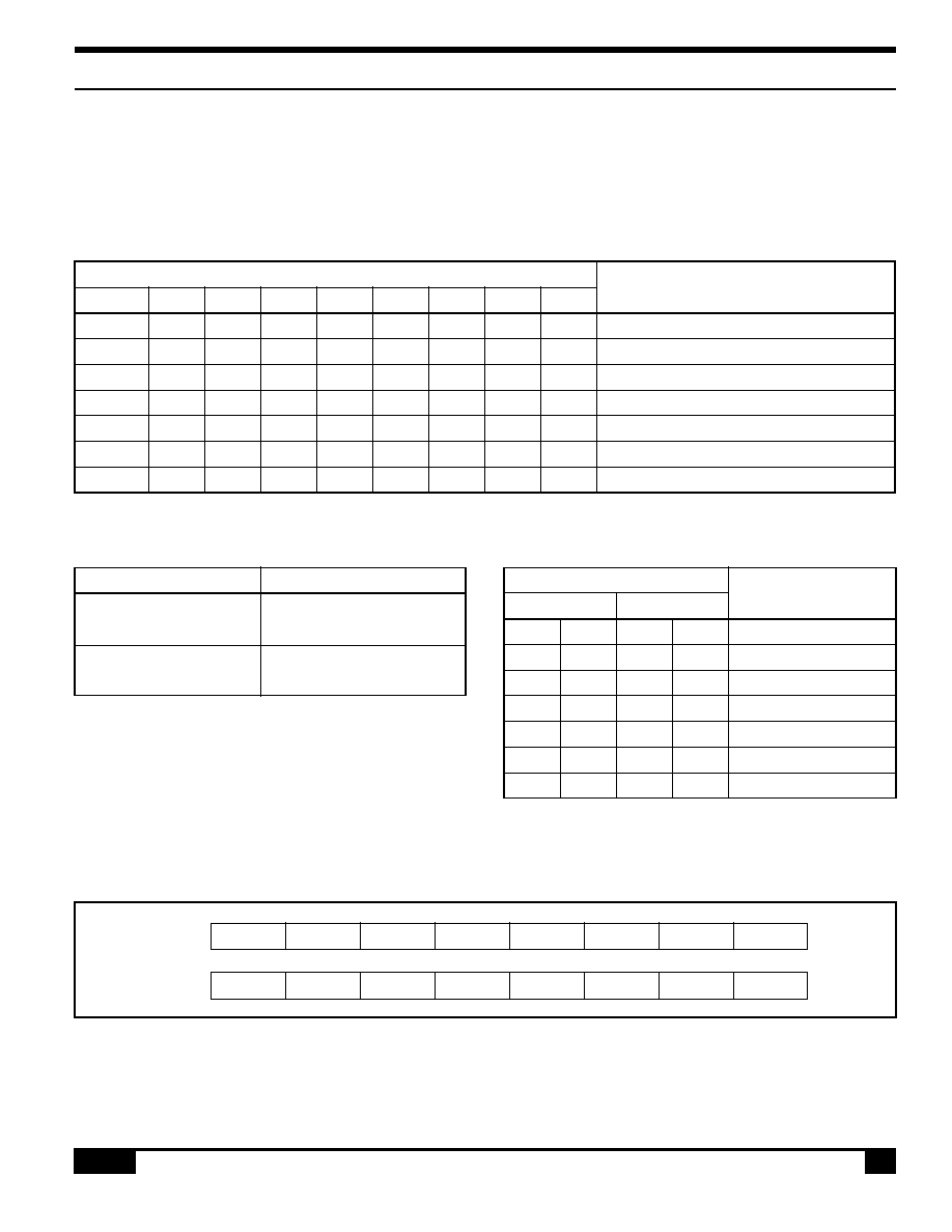
3.3 Display Control Commands ......................................................................................................... 36
3.3.1 DISP ON/OFF ......................................................................................................... 36
3.3.1.1 D ........................................................................................................ 37
3.3.1.2 FC ...................................................................................................... 37
3.3.1.3 FP ...................................................................................................... 37
3.3.2 SCROLL ................................................................................................................. 37
3.3.2.1 C ........................................................................................................ 37
3.3.2.2 SL1, SL2 ............................................................................................ 38
3.3.3 CSRFORM.............................................................................................................. 42
3.3.3.1 CRX ................................................................................................... 42
3.3.3.2 CRY .................................................................................................... 42
3.3.3.3 CM ..................................................................................................... 43
3.3.4 CSRDIR .................................................................................................................. 43
3.3.5 OVLAY .................................................................................................................... 43
3.3.5.1 MX0, MX1 .......................................................................................... 43
3.3.5.2 DM1, DM2 .......................................................................................... 45
3.3.5.3 OV ...................................................................................................... 45
3.3.6 CGRAM ADR .......................................................................................................... 45
3.3.7 HDOT SCR ............................................................................................................. 45
3.3.7.1 D0 to D2 ............................................................................................. 45
3.4 Drawing Control Commands ....................................................................................................... 46
3.4.1 CSRW ..................................................................................................................... 46
3.4.2 CSRR ...................................................................................................................... 46
3.5 Memory Control Commands ....................................................................................................... 47
3.5.1 MWRITE ................................................................................................................. 47
3.5.2 MREAD ................................................................................................................... 47
4.0 Specifications ................................................................................................... 49
4.1 Absolute Maximum Ratings ......................................................................................................... 51
4.1.1 SED1330 ................................................................................................................ 51
4.1.2 SED1335/SED1336 ................................................................................................ 51
4.2 SED 1330 Electrical Characteristics ............................................................................................ 52
4.3 SED1335/1336 Electrical Characteristics .................................................................................... 53
4.4 SED1330 Timing Diagrams ......................................................................................................... 54
4.4.1 System bus READ/WRITE timing I (8080) ............................................................. 54
4.4.1.1 SED1330F ......................................................................................... 54
4.4.2 System bus READ/WRITE timing II (6800) ............................................................ 55
4.4.2.1 SED1330F ......................................................................................... 55
4.4.3 Display memory READ timing ................................................................................ 56
4.4.3.1 SED1330F ......................................................................................... 56
4.4.4 Display memory WRITE timing ............................................................................... 57
4.4.4.1 SED1330F ......................................................................................... 57
4.4.5 LCD control timing .................................................................................................. 58
4.4.5.1 SED1330F ......................................................................................... 59

S-MOS Systems, Inc. · 2460 North First Street · San Jose, CA 95131 · Tel: (408) 922-0200 · Fax: (408) 922-0238
268-0.4
5
4.4.6 Oscillator timing ...................................................................................................... 60
4.4.6.1 SED1330F ......................................................................................... 60
4.4.7 Measurement circuit ............................................................................................... 61
4.5 SED1335/SED1336 AC Timing Diagrams ................................................................................... 62
4.5.1 8080 family Interface Timing ................................................................................... 62
4.5.1.1 SED1335F ......................................................................................... 62
4.5.1.2 SED1336F ......................................................................................... 63
4.5.2 6800 family Interface Timing ................................................................................... 64
4.5.2.1 SED1335F ......................................................................................... 65
4.5.2.2 SED1336F ......................................................................................... 65
4.5.3 Display Memory Read Timing ................................................................................. 66
4.5.3.1 SED1335F ......................................................................................... 66
4.5.3.2 SED1336F ......................................................................................... 67
4.5.4 Display Memory Write Timing ................................................................................. 68
4.5.4.1 SED1335F ......................................................................................... 69
4.5.4.2 SED1336F ......................................................................................... 70
4.5.5 SLEEP IN Command Timing .................................................................................. 71
4.5.5.1 SED1335F ......................................................................................... 71
4.5.5.2 SED1336F ......................................................................................... 71
4.5.6 External Oscillator Signal Timing ............................................................................ 72
4.5.6.1 SED1335F ......................................................................................... 72
4.5.6.2 SED1336F ......................................................................................... 72
4.5.7 E-1330 LCD Controller IC ........................................................................................................ 73
4.5.7.1 SED1335F ......................................................................................... 75
4.5.7.2 SED1336F ......................................................................................... 75
5.0 Display Control Functions .............................................................................. 77
5.1 Character Configuration .............................................................................................................. 79
5.2 Screen Configuration ................................................................................................................... 81
5.2.1 Screen Configuration .............................................................................................. 81
5.2.2 Display Address Scanning ...................................................................................... 81
5.2.3 Display Scan Timing ............................................................................................... 84
5.3 Cursor Control ............................................................................................................................. 85
5.3.1 Cursor Register Function ........................................................................................ 85
5.3.2 Cursor Movement ................................................................................................... 85
5.3.3 Cursor Display Layers ............................................................................................ 85
5.4 Memory to Display Relationship .................................................................................................. 87
5.5 Scrolling ....................................................................................................................................... 90
5.5.1 On-page Scrolling ................................................................................................... 90
5.5.2 Inter-page Scrolling ................................................................................................. 91
5.5.3 Horizontal Scrolling ................................................................................................. 92
5.5.4 Bidirectional Scrolling ............................................................................................. 93
5.5.5 Scroll Units.............................................................................................................. 93
Table of Contents
SED1330F/1335F/1336F

S-MOS Systems, Inc. · 2460 North First Street · San Jose, CA 95131 · Tel: (408) 922-0200 · Fax: (408) 922-0238
6
268-0.4
6.0 Character Generator ........................................................................................ 95
6.1 CG Characteristics ...................................................................................................................... 97
6.1.1 Internal Character Generator .................................................................................. 97
6.1.2 External Character Generator ROM ....................................................................... 97
6.1.3 Character Generator RAM ...................................................................................... 97
6.2 CG Memory Allocation................................................................................................................. 98
6.3 Setting the Character Generator Address ................................................................................... 99
6.3.1 M1 = 1 ................................................................................................................... 100
6.3.2 CG RAM Addressing Example .............................................................................. 100
6.4 Character Codes ....................................................................................................................... 101
7.0 TV Mode (SED1336F only) ............................................................................. 103
7.1 Sync Generator Circuit Timing .................................................................................................. 105
8.0 Description of Circuit Blocks ........................................................................ 109
8.1 Microprocessor Interface ........................................................................................................... 111
8.1.1 System Bus Interface............................................................................................ 111
8.1.1.1 8080 series ...................................................................................... 111
8.1.1.2 6800 series ...................................................................................... 111
8.1.2 Microprocessor Synchronization........................................................................... 111
8.1.2.1 Display Status Indication Output For SED1336F only...................... 111
8.1.2.2 Internal Register Access .................................................................. 111
8.1.2.3 Display Memory Access ................................................................... 111
8.1.3 Interface Examples ............................................................................................... 113
8.1.3.1 Z80® to SED1330F/1335F/1336F Interface .................................... 113
8.1.3.2 6802 to SED1330F/1335F/1336F Interface ..................................... 114
8.2 Display Memory Interface .......................................................................................................... 115
8.2.1 Static RAM ............................................................................................................ 115
8.2.2 Supply Current during Display Memory Access .................................................... 115
8.3 Oscillator Circuit ........................................................................................................................ 116
8.4 Status Flag ................................................................................................................................ 116
8.5 Reset ......................................................................................................................................... 117
9.0 Application Notes ........................................................................................... 119
9.1 Initialization Parameters ............................................................................................................ 121
9.1.1 SYSTEM SET Instruction and Parameters ........................................................... 121
9.1.2 Initialization Example ............................................................................................ 122
9.1.3 Display Mode Setting Example 1: Combining Text and Graphics ......................... 128
9.1.4 Display Mode Setting Example 2: Combining Graphics and Graphics ................. 129
9.1.5 Display Mode Setting Example 3: Combining Three Graphics Layers ................. 130
9.2 System Overview ...................................................................................................................... 132
SED1330F/1335F/1336F
Table of Contents

S-MOS Systems, Inc. · 2460 North First Street · San Jose, CA 95131 · Tel: (408) 922-0200 · Fax: (408) 922-0238
268-0.4
7
Table of Contents
SED1330F/1335F/1336F
9.3 System Interconnection ............................................................................................................. 133
9.3.1 SED1330F/1335F ................................................................................................. 133
9.3.2 SED1336F ............................................................................................................ 134
9.4 Smooth Horizontal Scrolling ...................................................................................................... 135
9.5 Layered Display Attributes ......................................................................................................... 137
9.5.1 Inverse Display ..................................................................................................... 137
9.5.2 Half-tone Display .................................................................................................. 137
9.5.2.1 Menu Pad Display ............................................................................ 137
9.5.2.2 Graph Display .................................................................................. 138
9.5.3 Flashing Areas ...................................................................................................... 138
9.5.3.1 Small Area ........................................................................................ 138
9.5.3.2 Large Area ....................................................................................... 138
9.6 16
×
16-dot Graphic Display ...................................................................................................... 139
9.6.1 Command Usage .................................................................................................. 139
9.6.2 Kanji Character Display ........................................................................................ 139
10.0 Internal Character Generator Font ............................................................. 141
11.0 Glossary of Terms ........................................................................................ 145

S-MOS Systems, Inc. · 2460 North First Street · San Jose, CA 95131 · Tel: (408) 922-0200 · Fax: (408) 922-0238
8
268-0.4
SED1330F/1335F/1336F
Table of Contents
THIS PAGE INTENTIONALLY BLANK

S-MOS Systems, Inc. · 2460 North First Street · San Jose, CA 95131 · Tel: (408) 922-0200 · Fax: (408) 922-0238
268-0.4
9
1.0
Overview

S-MOS Systems, Inc. · 2460 North First Street · San Jose, CA 95131 · Tel: (408) 922-0200 · Fax: (408) 922-0238
10
268-0.4
THIS PAGE INTENTIONALLY BLANK

S-MOS Systems, Inc. · 2460 North First Street · San Jose, CA 95131 · Tel: (408) 922-0200 · Fax: (408) 922-0238
268-0.4
11
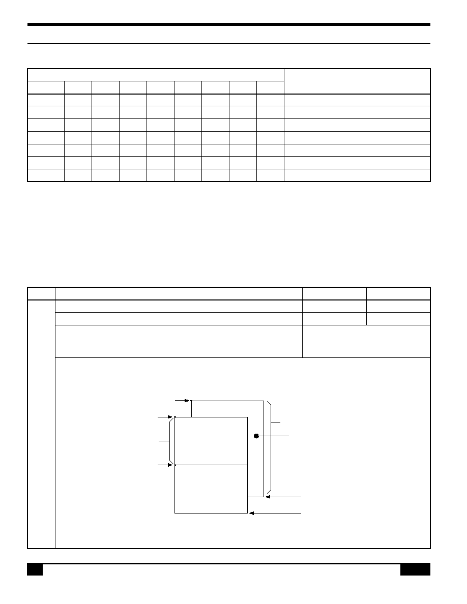
1.0 1.2
1.0 Overview
1.0 Overview
1.1 Description
The SED1330/1335F/1336F is a family of versatile
LCD controller ICs that can display text and graphics
on a medium size LCD panel. The software is
compatible among all three chips. S-MOS recom-
mends new designs use the SED1335 since the
SED1330 will gradually be replaced by the SED1335.
The SED1336F incorporates a TV sync generator
circuit that is compatible with both NTSC and PAL
systems. The 256
×
200 pixel TV display comprises
three superimposed layers, and is identical to the
simultaneous LCD panel display. When driving an
LCD only, up to 3 overlapping layers can be displayed
on LCD panels up to 640
×
256 pixels in size. The
SED1330/1335F does not incorporate a TV controller.
The SED1330/1335F/1336F can display layered text
and graphics, scroll the display in any direction and
partition the display into multiple screens.
The SED1330/1335F/1336F stores text, character
codes and bit-mapped graphics data in external frame
buffer memory. Display controller functions include
transferring data from the controlling microprocessor
to the buffer memory, reading memory data, convert-
ing data to display pixels and generating timing sig-
nals for the buffer memory, TV monitor and LCD
panel.
The SED1330/1335F/1336F has an internal charac-
ter generator with 160, 5
×
7 pixel characters in
internal mask ROM. The character generators sup-
port up to 64, 8
×
16 pixel characters in external
character generator RAM and up to 256, 8
×
16 pixel
characters in external character generator ROM.
1.2 Features
· Text, graphics and combined text/graphics dis-
play modes
· Three overlapping screens in graphics mode
· 640
×
256 pixel LCD panel display resolution
· Programmable cursor control
· Smooth horizontal and vertical scrolling of all or
part of the display
· 1/2-duty to 1/256-duty LCD drive
· Up to 64 Kbytes of external static RAM frame
buffer memory
· Internal character generator
· 160, 5
×
7 pixel characters in internal mask-
programmed character generator ROM
· Up to 64, 8
×
16 pixel characters in external
character generator RAM
· Up to 256, 8
×
16 pixel characters in external
character generator ROM
· 6800 and 8080 family microprocessor inter-
faces
· NTSC and PAL systems compatible
(SED1336F only)
· 256
×
200 pixel TV monitor display resolution
(SED1336F only)
· Low power consumption--3.5 mA operating
current (V
DD
= 3.5V), 0.05
µ
A standby current
· 4.5 to 5.5V (SED1330F)
· 2.7 to 5.5V (SED1330F/1335F)
· 3.0 to 5.5V (SED1336F)
· Available in 60-pin QFPs
S-MOS Systems, Inc. · 2460 North First Street · San Jose, CA 95131 · Tel: (408) 922-0200 · Fax: (408) 922-0238
12
268-0.4
1.0 Overview
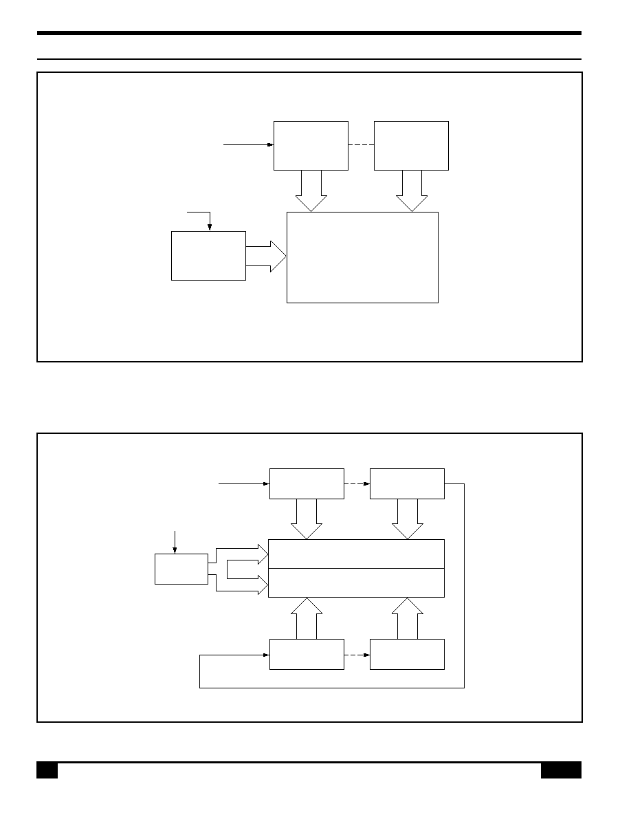
1.3
1.3 Block Diagram
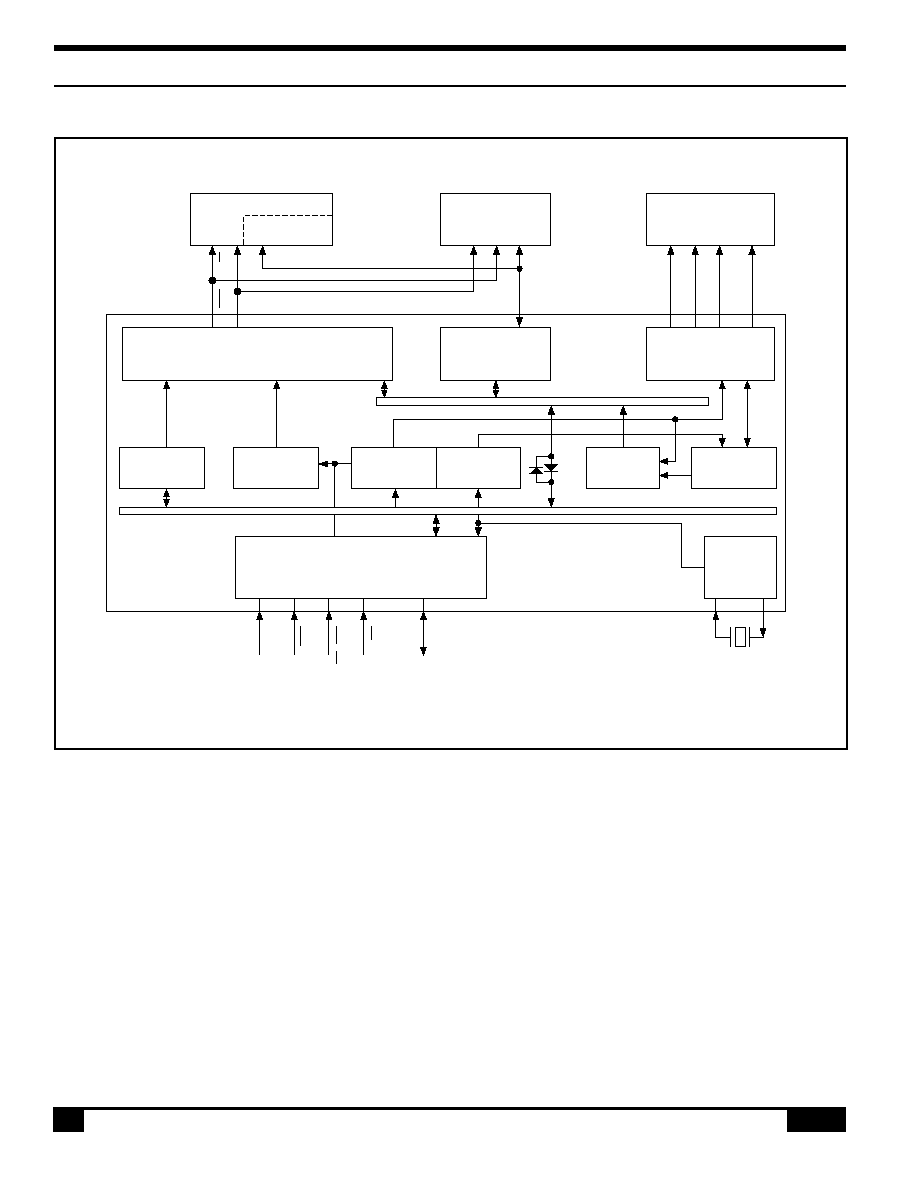
Figure 1. SED1330F block diagram
Video RAM
Character
Generator RAM
Character
Generator ROM
LCD
LCD Controller
Input/Output
Register
Video RAM Interface
Display
Address
Controller
Cursor
Address
Controller
Refresh
Counter
Dot Counter
Layered
Controller
Character
Generator
ROM
Oscillator
Microprocessor Interface
YSCL,YD,YDIS
LP, WF
XSCL, XECL
XD0 to XD3
VD0 to VD7
VA0 to VA15
VCE
VR/W
SEL1
SEL0
RES
RD, WR
A0, CS
D0 to D7
OSC1
OSC2
S-MOS Systems, Inc. · 2460 North First Street · San Jose, CA 95131 · Tel: (408) 922-0200 · Fax: (408) 922-0238
268-0.4
13
1.3 Block Diagram
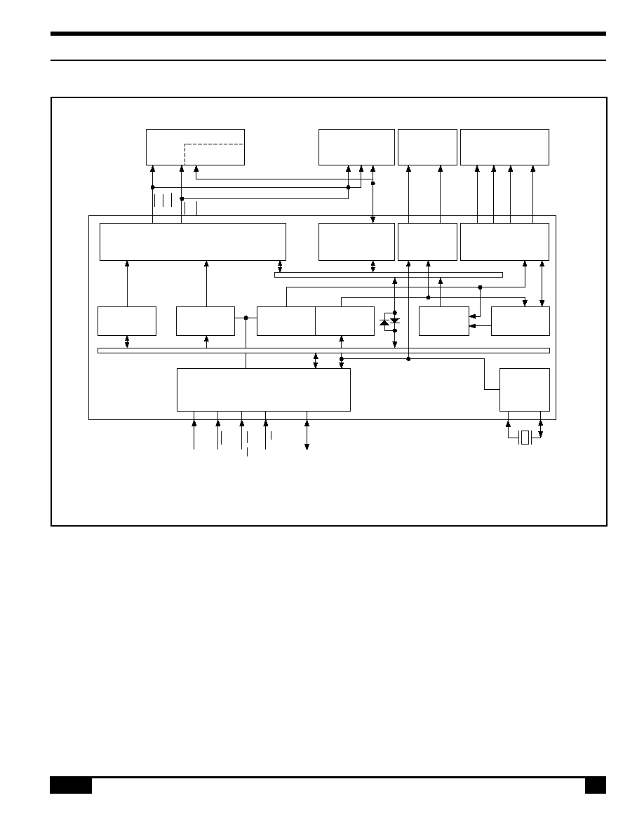
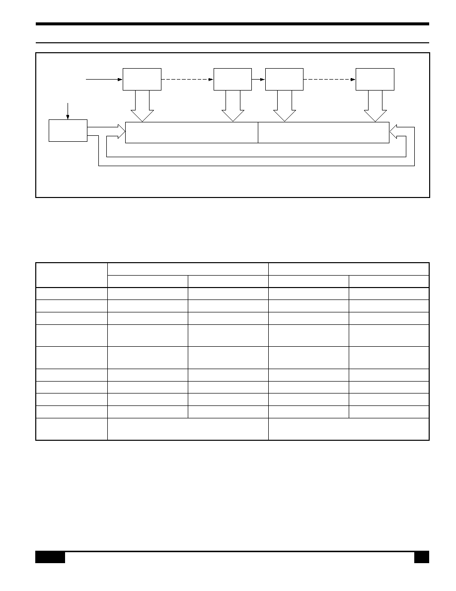
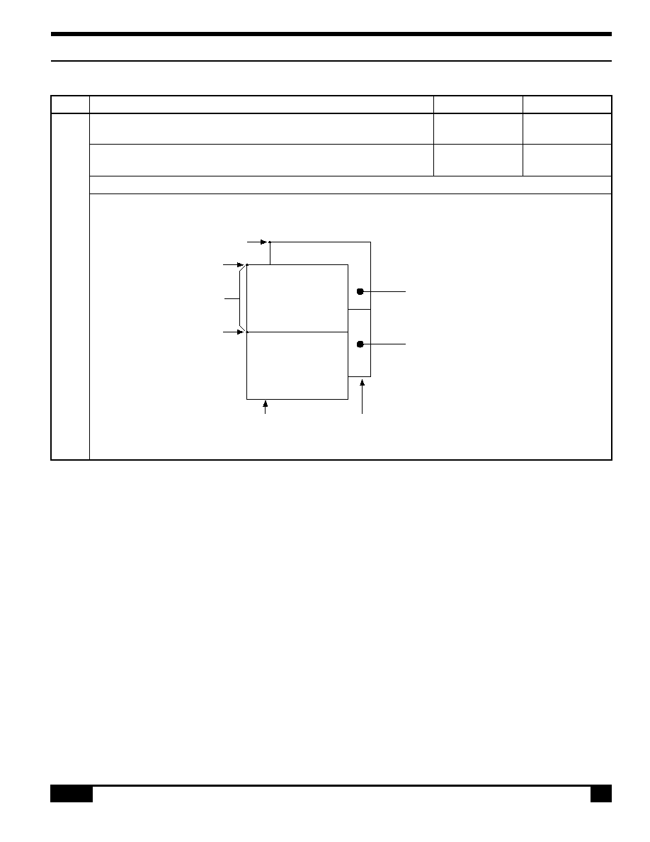
Figure 2. SED1335F/1336F block diagram
1.3
1.0 Overview
Video RAM
Character
Generator RAM
Character
Generator ROM
LCD Controller
Video RAM Interface
Display
Address
Controller
Cursor
Address
Controller
Refresh
Counter
Dot Counter
Character
Generator
ROM
Layered
Controller
Oscillator
Microprocessor Interface
YSCL, YD, YDIS
LP, WF
XSCL, XECL
XD0 to XD3
VD0 to VD7
VA0 to VA15
VCE,
VRD,
VWR
VRD
VWR
SEL1
SEL0
RES
RD, WR
A0, CS
D0 to D7
XG
XD
TV
Controller*
Input/Output
Register
TV
LCD
VSD
SNC
*SED1336F only
S-MOS Systems, Inc. · 2460 North First Street · San Jose, CA 95131 · Tel: (408) 922-0200 · Fax: (408) 922-0238
14
268-0.4
1.0 Overview
1.4 1.4.2
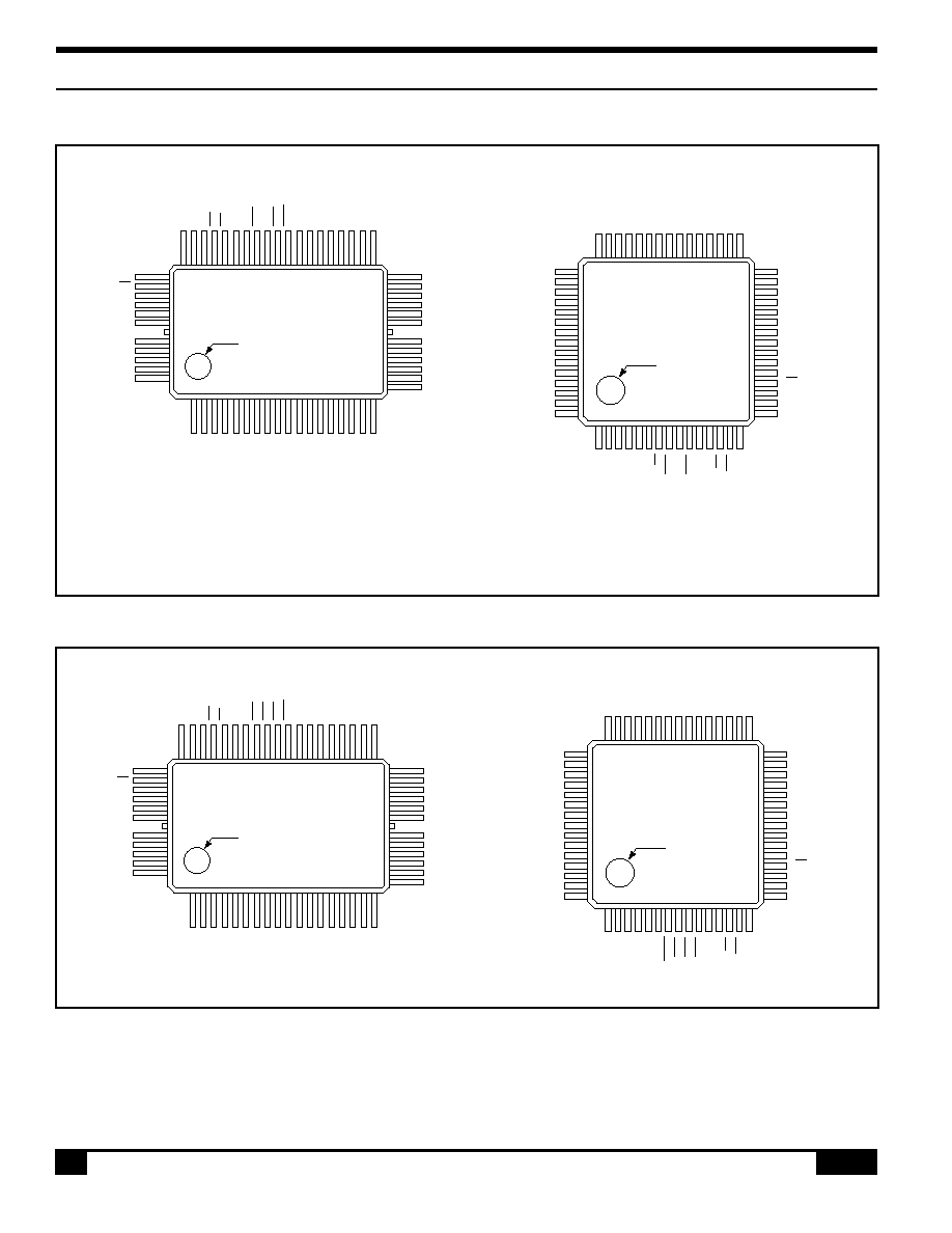
1.4 Pinouts
Index
1
15
31
45
46
60
SED1330F
BB
16
30
XD3
D7
D6
D5
D4
D3
D2
D1
D0
V
DD
A0
CS
OSC2
OSC1
SEL 1
VD3
VD2
VD1
VD0
VA15
VA14
VA13
VA12
VA11
VA10
VA9
VA8
VA7
VA6
NC
VD4
VD5
VD6
VD7
YSCL
YD
YDIS
WF
LP
V
SS
XSCL
XECL
XD0
XD1
XD2
VA5
VA4
VA3
VA2
VA1
VA0
VR/W
VCE
NC
RES
NC
NC
RD
WR
SEL 2
Index
55
1
30
60
5
29
40
45
50
20
15
10
SED1330F
BA
VA8
VA9
VA10
VA11
VA12
VA13
NC
VA14
VA15
VD0
VD1
VD2
XD
CS
A0
V
DD
D0
D1
D2
D3
D4
D5
D6
D7
XD3
XD2
XD1
XD0
XECL
XSCL
V
SS
LP
WF
YDIS
YD
YSCL
VD7
VD6
VD5
VD4
VD3
XG
SEL1
SEL2
WR
RD
NC
NC
RES
NC
VCE
VWR
VA0
VA1
VA2
VA3
VA4
VA5
VA6
VA7
6
Figure 3. SED1330F and SED1335F pinouts
Index
1
15
31
45
46
60
SED1335F
0B
(SED1336F
0A
)
16
30
XD3
D7
D6
D5
D4
D3
D2
D1
D0
V
DD
A0
CS
XD
XG
SEL1
VD3
VD2
VD1
VD0
VA15
VA14
VA13
VA12
VA11
VA10
VA9
VA8
VA7
VA6
NC
VD4
VD5
VD6
VD7
YSCL(SNC)
YD
YDIS
WF
LP
V
SS
XSCL
XECL(VSD)
XD0
XD1
XD2
VA5
VA4
VA3
VA2
VA1
VA0
VWR
VCE
VRD
RES
NC
NC(CLO)
RD
WR
SEL 2(NT/PL)
Index
55
1
30
60
5
29
40
45
50
20
15
10
SED1335F
OA
VA8
VA9
VA10
VA11
VA12
VA13
NC
VA14
VA15
VD0
VD1
VD2
XD
CS
A0
V
DD
D0
D1
D2
D3
D4
D5
D6
D7
XD3
XD2
XD1
XD0
XECL
XSCL
V
SS
LP
WF
YDIS
YD
YSCL
VD7
VD6
VD5
VD4
VD3
XG
SEL1
SEL2
WR
RD
NC
NC
RES
VRD
VCE
VWR
VA0
VA1
VA2
VA3
VA4
VA5
VA6
VA7
6
S-MOS Systems, Inc. · 2460 North First Street · San Jose, CA 95131 · Tel: (408) 922-0200 · Fax: (408) 922-0238
268-0.4
15
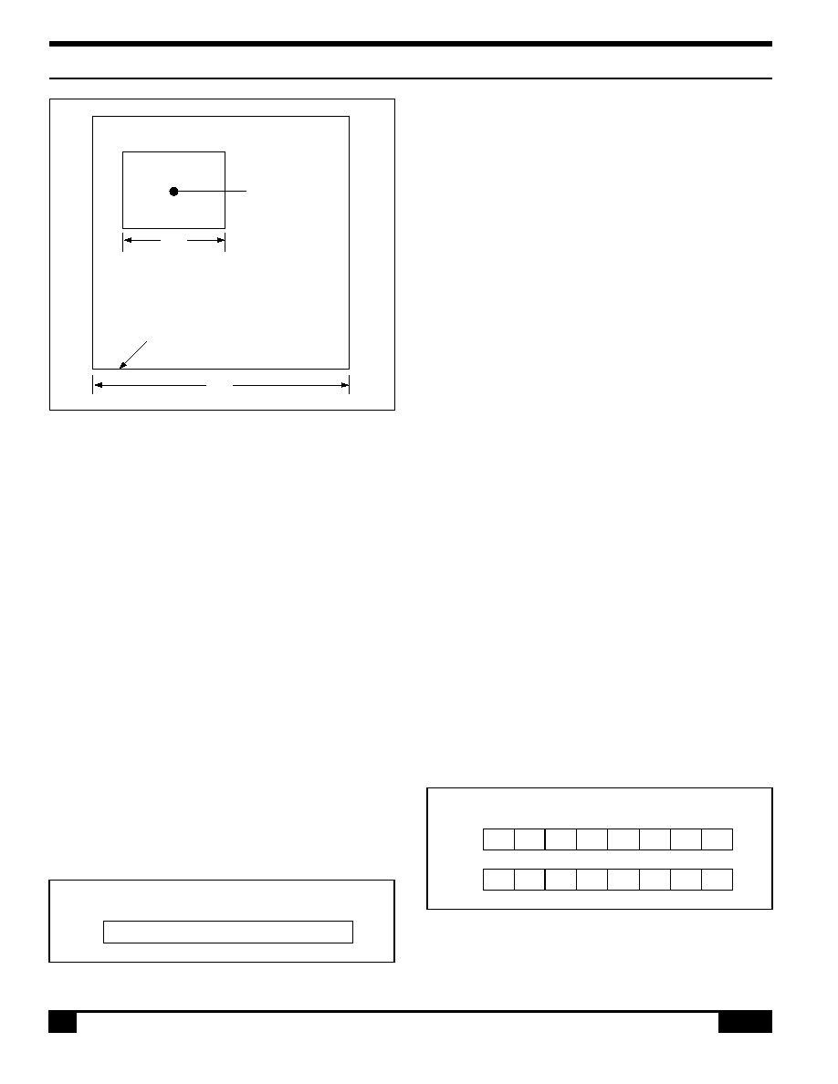
1.5 Package Dimensions
QFP5
Unit: mm
Figure 5. SED1330F
BB
, 1335F
0B
and SED1336F
0A
QFP6
Unit: mm
Index
1
15
31
16
45
46
60
30
0 ~ 12
°
1.8
2.7
±
0.1
0.8
±
0.3
0.15
±
0.05
0.35
±
0.15
0.8
±
0.15
17.6
±
0.4
14.0
±
0.2
17.6
±
0.4
14.0
±
0.2
0 ~ 12
°
2.8
2.7
±
0.1
1.5
±
0.3
0.15
±
0.05
Index
6
23
36
24
54
55
1
30
0.35
±
0.1
19.6
±
0.4
14.0
±
0.1
25.6
±
0.4
20.0
±
0.1
60
5
29
35
1.0
±
0.1
Figure 4. SED1330F
BA
and 1335F
0A
package dimensions
1.4 1.4.2
1.0 Overview

S-MOS Systems, Inc. · 2460 North First Street · San Jose, CA 95131 · Tel: (408) 922-0200 · Fax: (408) 922-0238
16
268-0.4
THIS PAGE INTENTIONALLY BLANK

S-MOS Systems, Inc. · 2460 North First Street · San Jose, CA 95131 · Tel: (408) 922-0200 · Fax: (408) 922-0238
268-0.4
17
2.0
Pin Description
S-MOS Systems, Inc. · 2460 North First Street · San Jose, CA 95131 · Tel: (408) 922-0200 · Fax: (408) 922-0238
18
268-0.4
2.0 Pin Description
2.1 SED1330F
BA/BB
Pin Summary
2.0 Pin Description
2.0 2.1
Name
Number
Type
Description
SED1330F
0A
SED1330F
BB
VA0 to VA15
27 to 28
50 to 59
Output
VRAM address bus
30 to 43
1 to 6
VR/W
44
7
Output
VRAM write signal
VCE
45
8
Output
Memory control signal
RES
47
10
Input
Reset
NC
29, 46, 48, 49
9, 11, 12, 60
--
No connection
RD
50
13
Input
8080 family: Read signal
6800 family: Enable clock (E)
WR
51
14
Input
8080 family: Write signal
6800 family: R/W signal
SEL2
52
15
Input
8080 or 6800 family interface
select
SEL1
53
16
Input
8080 or 6800 family interface
select
OSC1
54
17
Input
Oscillator connection
OSC2
55
18
Output
Oscillator connection
CS
56
19
Input
Chip select
A0
57
20
Input
Data type select
V
DD
58
21
Supply
4.5 to 5.5V supply
D0 to D7
59 to 60
22 to 29
Input/output
Data bus
1 to 6
XD0 to XD3
10 to 7
33 to 30
Output
X-driver data
XECL
11
34
Output
X-driver enable chain clock
XSCL
12
35
Output
X-driver data shift clock
V
SS
13
36
Supply
Ground
LP
14
37
Output
Latch pulse
WF
15
38
Output
Frame signal
YDIS
16
39
Output
Power-down signal when display is
blanked
YD
17
40
Output
Scan start pulse
YSCL
18
41
Output
Y-driver shift clock
VD0 to VD7
26 to 19
49 to 42
Input/output
VRAM data bus
S-MOS Systems, Inc. · 2460 North First Street · San Jose, CA 95131 · Tel: (408) 922-0200 · Fax: (408) 922-0238
268-0.4
19
2.0 2.2
2.0 Pin Description
2.0 Pin Description
2.2 SED1330F/1335F
0A/0B
Pin Summary
Name
Number
Type
Description
SED1335F
0A
SED1335F
0B
VA0 to VA15
27 to 28
50 to 59
Output
VRAM address bus
30 to 43
1 to 6
VWR
44
7
Output
VRAM write signal
VCE
45
8
Output
Memory control signal
VRD
46
9
Output
VRAM read signal
RES
47
10
Input
Reset
NC
29, 48, 49
11, 12, 60
--
No connection
RD
50
13
Input
8080 family: Read signal
6800 family: Enable clock (E)
WR
51
14
Input
8080 family: Write signal
6800 family: R/W signal
SEL2
52
15
Input
8080 or 6800 family interface
select
SEL1
53
16
Input
8080 or 6800 family interface
select
XG
54
17
Input
Oscillator connection
XD
55
18
Output
Oscillator connection
CS
56
19
Input
Chip select
A0
57
20
Input
Data type select
V
DD
58
21
Supply
2.7 to 5.5V supply
D0 to D7
59 to 60
22 to 29
Input/output
Data bus
1 to 6
XD0 to XD3
10 to 7
33 to 30
Output
X-driver data
XECL
11
34
Output
X-driver enable chain clock
XSCL
12
35
Output
X-driver data shift clock
V
SS
13
36
Supply
Ground
LP
14
37
Output
Latch pulse
WF
15
38
Output
Frame signal
YDIS
16
39
Output
Power-down signal when display is
blanked
YD
17
40
Output
Scan start pulse
YSCL
18
41
Output
Y-driver shift clock
VD0 to VD7
26 to 19
49 to 42
Input/output
VRAM data bus
S-MOS Systems, Inc. · 2460 North First Street · San Jose, CA 95131 · Tel: (408) 922-0200 · Fax: (408) 922-0238
20
268-0.4
2.0 Pin Description
2.3
2.3 SED1336F
0A
Pin Summary
Name
Number
Type
Description
VA0 to VA15
1 to 6
Output
VRAM address bus
50 to 59
VWR
7
Output
VRAM write signal
VCE
8
Output
Memory control signal
VRD
9
Output
VRAM read signal
RES
10
Input
Reset
NC
11, 60
--
No connection
CLO
12
Output
Clock output
RD
13
Input
8080 family: Read signal
6800 family: Enable clock (E)
WR
14
Input
8080 family: Write signal
6800 family: R/W signal
NT/PL
15
Input
NTSC or PAL TV mode select
SEL1
16
Input
8080 or 6800 family interface select
OSC1
17
Input
Oscillator connection
OSC2
18
Output
Oscillator connection
CS
19
Input
Chip select
A0
20
Input
Data type select
V
DD
21
Supply
3.0 to 5.5V supply
D0 to D7
22 to 29
Input/output
Data bus
XD0 to XD3
30 to 33
Output
X-driver data
VSD
34
Output
Video data
XSCL
35
Output
Data shift clock
V
SS
36
Supply
Ground
LP
37
Output
Latch pulse
WF
38
Output
Frame signal
YDIS
39
Output
Power-down signal when display is
blanked
YD
40
Output
Scan start pulse
SNC
41
Output
TV sync signal
VD0 to VD7
42 to 49
Input/output
VRAM data bus
S-MOS Systems, Inc. · 2460 North First Street · San Jose, CA 95131 · Tel: (408) 922-0200 · Fax: (408) 922-0238
268-0.4
21
2.4 2.4.3
2.0 Pin Description
2.4 Pin Functions
2.4.1 Power Supply
Pin Name
Function
V
DD
4.5 to 5.5V (SED1330F), 3.0 to 5.5V (SED1336F) or 2.7 to 5.5V (SED1330F/1335F) supply.
This may be the same supply as the controlling microprocessor.
V
SS
Ground
Note: The peak supply current drawn by the SED1330F/1335F/1336F may be up to ten times the average supply current. The power
supply impedance must be kept as low as possible by ensuring that supply lines are sufficiently wide and by placing 0.47
µ
F
decoupling capacitors that have good high-frequency response near the device's supply pins.
2.4.3 Microprocessor Interface
Pin Name
Function
D0 to D7
Tristate input/output pins. Connect these pins to an 8- or 16-bit microprocessor bus.
Microprocessor interface select pin. The SED1336F supports both 8080 family processors
(such as the 8085 and Z80®) and 6800 family processors (such as the 6802 and 6809).
SEL1*
SEL2
Interface
A0
RD
WR
CS
0
0
8080 family
A0
RD
WR
CS
1
0
6800 family
A0
E
R/W
CS
* SED1330F and SED1335F only
Note: SEL1 should be tied directly to V
DD
or V
SS
to prevent noise. If noise does appear on SEL1, decouple it to ground using a
capacitor placed as close to the pin as possible.
SEL1, SEL2
2.4.2 Oscillator
Pin Name
Function
(OSC) XG
Crystal connection for internal oscillator (see Section 8.3). This pin can be driven by an external
clock source that satisfies the timing specifications of the EXT
0 signal (see Section 4.3.6).
(OSC2) XD
Crystal connection for internal oscillator. Leave this pin open when using an external clock
source.
CLO
Clock output (SED1336F only). Same phase as XG. Clock is output when system command
P1 is executed. Output stops during system reset.
S-MOS Systems, Inc. · 2460 North First Street · San Jose, CA 95131 · Tel: (408) 922-0200 · Fax: (408) 922-0238
22
268-0.4
2.0 Pin Description
2.4.3
Pin Name
Function
A0, in conjunction with the RD and WR or R/W and E signals, controls the type of access to
the SED1336F, as shown below.
8080 family interface
A0
RD
WR
Function
0
0
1
Status flag read
1
0
1
Display data and cursor address read
0
1
0
Display data and parameter write
1
1
0
Command write
6800 family interface
A0
R/W
E
Function
0
1
1
Status flag read
1
1
1
Display data and cursor address read
0
0
1
Display data and parameter write
1
0
1
Command write
When the 8080 family interface is selected, this signal acts as the active-LOW read strobe. The
SED1330F/1335F/1336F's output buffers are enabled when this signal is active.
When the 6800 family interface is selected, this signal acts as the active-HIGH enable clock.
Data is read from or written to the SED1330F/1335F/1336F when this clock goes HIGH.
When the 8080 family interface is selected, this signal acts as the active-LOW write strobe. The
bus data is latched on the rising edge of this signal.
When the 6800 family interface is selected, this signal acts as the read/write control signal. Data
is read from the SED1330F/1335F/1336F if this signal is HIGH, and written to the SED1330F/
1335F/1336F if it is LOW.
Chip select. This active-LOW input enables the SED1330F/1335F/1336F. It is usually
connected to the output of an address decoder device that maps the SED1330F/1335F/1336F
into the memory space of the controlling microprocessor.
This active-LOW input performs a hardware reset on the SED1330F/1335F/1336F. It is a
Schmitt-trigger input for enhanced noise immunity; however, care should be taken to ensure
that it is not triggered if the supply voltage is lowered.
WR or R/W
CS
RES
RD or E
A0
S-MOS Systems, Inc. · 2460 North First Street · San Jose, CA 95131 · Tel: (408) 922-0200 · Fax: (408) 922-0238
268-0.4
23
2.4.4 2.4.5
2.0 Pin Description
2.4.4 Display Memory Control
The SED1330F/1335F/1336F can directly access static
RAM and PROM. The designer may use a mixture of
these two types of memory to achieve an optimum
trade-off between low cost and low power consumption.
Pin Name
Function
VA0 to VA15
16-bit display memory address. When accessing character generator RAM or ROM, VA0 to
VA3, reflect the lower 4 bits of the row counter.
VD0 to VD7
8-bit tristate display memory data bus. These pins are enabled when VR/W is LOW.
VR/W
Active-LOW display memory write control output (SED1330).
VRD
Active-LOW display memory read control output (SED1335/6).
VCE
Active-LOW static memory standby control signal. VCE can be used with CS.
VWR
Active-LOW display memory write control output (SED1335/6).
2.4.5 LCD Drive Signals
In order to provide effective low-power drive for LCD
matrixes, the SED1330F/1335F/1336F can directly
control both the X- and Y-drivers using an enable
chain.
Pin Name
Function
XD0 to XD3
4-bit X-driver (column drive) data outputs. Connect these outputs to the inputs of the X-driver
chips.
The falling edge of XSCL latches the data on XD0 to XD3 into the input shift registers of the
X-drivers. To conserve power, this clock halts between LP and the start of the following display
line (see Section 4.3.7).
XECL
The falling edge of XECL (SED1330F/1335F only) triggers the enable chain cascade for the
X-drivers (SED1600/SED1180). Every 16th clock pulse is output to the next X-driver.
LP latches the signal in the X-driver shift registers into the output data latches. LP is a falling-
edge triggered signal, and pulses once every display line.
Connect LP to the Y-driver shift clock on modules that use the SED1600 and SED1610 drivers.
WF
LCD panel AC drive output. The WF period is selected to be one of two values with SYSTEM
SET command.
The falling edge of YSCL (SED1330F/1335F only) latches the data on YD into the input shift
registers of the Y-drivers. YSCL is not used with the SED1600, SED1610 or other driver ICs
which use LP as the Y-driver shift clock.
YD is the data pulse output for the Y drivers. It is active during the last line of each frame, and
is shifted through the Y drivers one by one (by YSCL), to scan the display's common
connections.
Power-down output signal. YDIS is HIGH while the display drive outputs are active.
YDIS goes LOW one or two frames after the sleep command is written to the SED1330F/
1335F/1336F. All Y-driver outputs are forced to an intermediate level (de-selecting the display
segments) to blank the display. In order to implement power-down operation in the LCD unit,
the LCD power drive supplies must also be disabled when the display is disabled by YDIS.
XSCL
LP
YSCL
YD
YDIS

S-MOS Systems, Inc. · 2460 North First Street · San Jose, CA 95131 · Tel: (408) 922-0200 · Fax: (408) 922-0238
24
268-0.4
1.0 Overview
1.3
THIS PAGE INTENTIONALLY BLANK

S-MOS Systems, Inc. · 2460 North First Street · San Jose, CA 95131 · Tel: (408) 922-0200 · Fax: (408) 922-0238
268-0.4
25
1.3 1.4
1.0 Overview
3.0
Command Description

S-MOS Systems, Inc. · 2460 North First Street · San Jose, CA 95131 · Tel: (408) 922-0200 · Fax: (408) 922-0238
26
268-0.4
THIS PAGE INTENTIONALLY BLANK
S-MOS Systems, Inc. · 2460 North First Street · San Jose, CA 95131 · Tel: (408) 922-0200 · Fax: (408) 922-0238
268-0.4
27
3.0 3.1
3.0 Command Description
3.0 Command Description
3.1 The Command Set
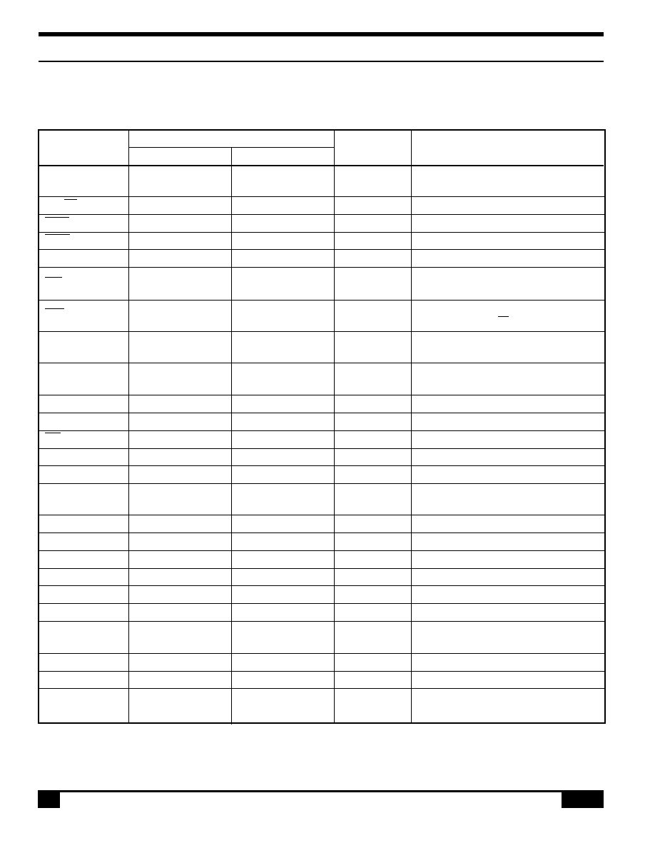
Table 1. The Command Set
Command
Code
Read
Class
Command
Hex Command Description
Parameters
RD WR A0 D7 D6 D5 D4 D3 D2 D1 D0
No. of
Sec-
Bytes
tion
SYSTEM SET
1
0
1
0
1
0
0
0
0
0
0
40
Initialize device and dis-
8
3.2.1
play
SLEEP IN
1
0
1
0
1
0
1
0
0
1
1
53
Enter standby mode
0
3.2.2
DISP ON/OFF
1
0
1
0
1
0
1
1
0
0
D
58, Enable and disable dis-
1
3.3.1
59
play and display flashing
SCROLL
1
0
1
0
1
0
0
0
1
0
0
44
Set display start address
10
3.3.2
and display regions
CSRFORM
1
0
1
0
1
0
1
1
1
0
1
5D Set cursor type
2
3.3.3
CGRAM ADR
1
0
1
0
1
0
1
1
1
0
0
5C
Set start address of char-
2
3.3.6
acter generator RAM
CD CD
4C
Set direction of cursor
CSRDIR
1
0
1
0
1
0
0
1
1
1
0
to
movement
0
3.3.4
4F
HDOT SCR
1
0
1
0
1
0
1
1
0
1
0
5A
Set horizontal scroll pos-
1
3.3.7
ition
OVLAY
1
0
1
0
1
0
1
1
0
1
1
5B
Set display overlay for-
1
3.3.5
mat
CSRW
1
0
1
0
1
0
0
0
1
1
0
46
Set cursor address
2
3.4.1
CSRR
1
0
1
0
1
0
0
0
1
1
1
47
Read cursor address
2
3.4.2
MWRITE
1
0
1
0
1
0
0
0
0
1
0
42
Write to display memory
--
3.5.1
MREAD
1
0
1
0
1
0
0
0
0
1
1
43
Read from display mem-
--
3.5.2
ory
Notes:
1. In general, the internal registers of the SED1330F/1335F/1336F are modified as each command parameter is input. However,
the microprocessor does not have to set all the parameters of a command and may send a new command before all parameters
have been input. The internal registers for the parameters that have been input will have been changed but the remaining
parameter registers are unchanged.
2-byte parameters (where two bytes are treated as one data item) are handled as follows:
a. CSRW, CSRR: Each byte is processed individually. The microprocessor may read or write just the low byte of the cursor
address.
b. SYSTEM SET, SCROLL, CGRAM ADR: Both parameter bytes are processed together. If the command is changed after
half of the parameter has been input, the single byte is ignored.
2. APL and APH are 2-byte parameters, but are treated as two 1-byte parameters.
System
control
Display
control
Drawing
control
Memory
control
S-MOS Systems, Inc. · 2460 North First Street · San Jose, CA 95131 · Tel: (408) 922-0200 · Fax: (408) 922-0238
28
268-0.4
3.0 Command Description
3.2 3.2.1
3.2 System Control Commands
3.2.1 SYSTEM SET
Initializes the device, sets the window sizes, and
selects the LCD interface format. Since the command
sets the basic operating parameters of the SED1330F/
1335F/1336F, an incorrect SYSTEM SET command
may cause other commands to operate incorrectly.
C
0
1
0
0
0
0
0
0
1
0
1
D7
D6
D5
D4
D3
D2
D1
D0
A0
WR
RD
P1
DR
T/L
IV
1
W/S
M2
M1
M0
0
0
1
P2
WF
0
0
0
0
FX
0
0
1
P3
0
0
0
0
FY
0
0
1
P4
C/R
0
0
1
P5
TC/R
0
0
1
P6
L/F
0
0
1
P7
APL
0
0
1
P8
APH
0
0
1
LSB
MSB
Figure 7. SYSTEM SET instruction

S-MOS Systems, Inc. · 2460 North First Street · San Jose, CA 95131 · Tel: (408) 922-0200 · Fax: (408) 922-0238
268-0.4
29
3.2.1.1 3.2.1.5
3.0 Command Description
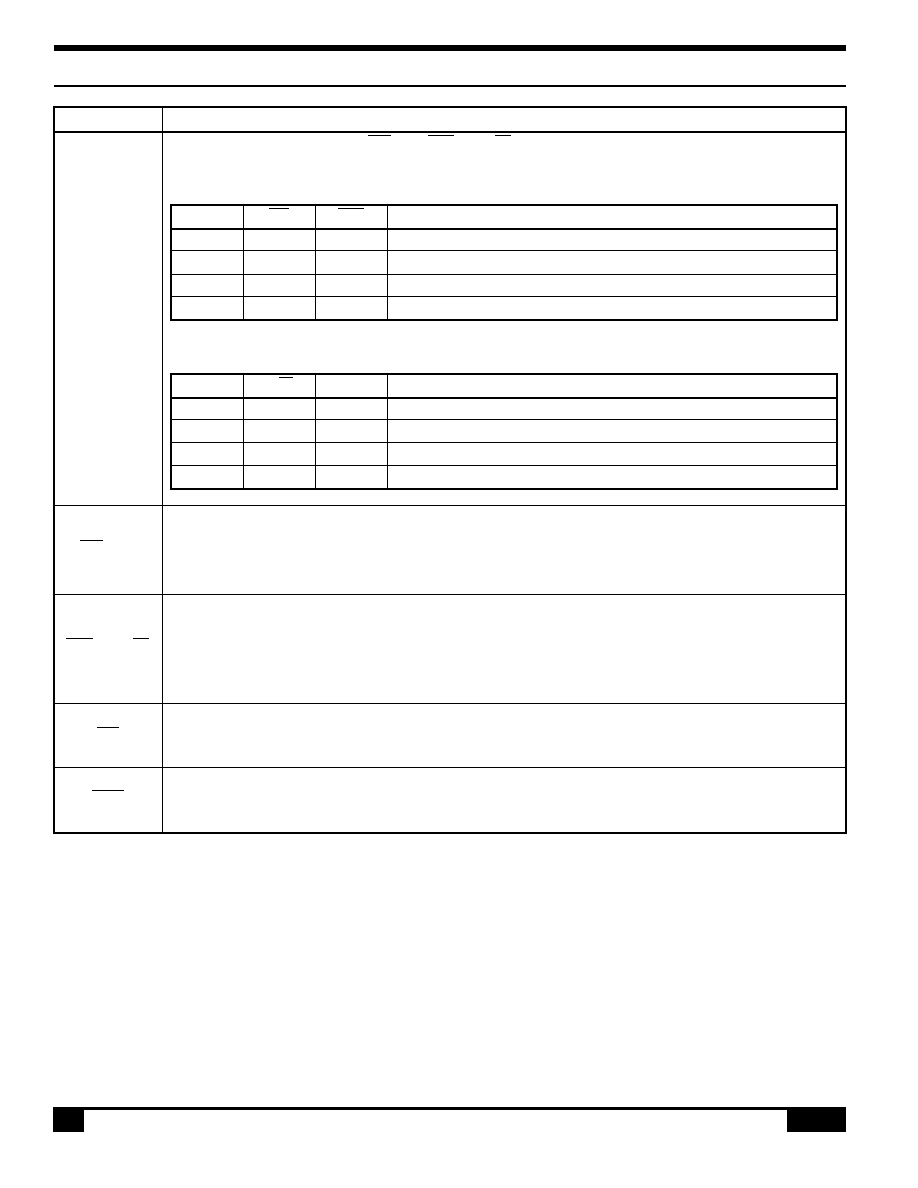
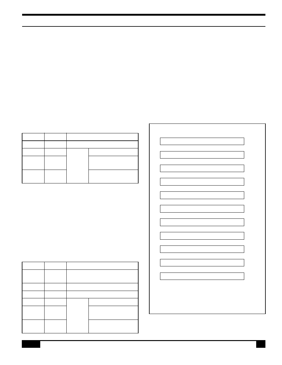
3.2.1.1 C
This control byte performs the following:
1. Resets the internal timing generator
2. Disables the display
3. Cancels sleep mode
Parameters following P1 are not needed if only can-
celing sleep mode.
3.2.1.2 M0
Selects the internal or external character generator
ROM. The internal character generator ROM con-
tains 160, 5
×
7 pixel characters. These characters are
fixed at fabrication by the metalization mask. The
external character generator ROM can contain up to
256 user-defined characters.
M0 = 0: Internal CG ROM
M0 = 1: External CG ROM
Note that if the CG ROM address space overlaps the
display memory address space, that portion of the
display memory cannot be written to.
3.2.1.3 M1
Selects the CG RAM area for user-definable charac-
ters. The CG RAM codes are selected from the 64
codes shown in Figure 59.
M1 = 0: CG RAM1; 32 char
The CG RAM1 and CG RAM2 address spaces are not
contiguous, the CG RAM1 address space is treated
as character generator RAM, and the CG RAM2
address space is treated as character generator ROM.
M1 = 1: 64 char CG RAM + CG RAM2
The CG RAM1 and CG RAM2 address spaces are
contiguous and are both treated as character genera-
tor RAM.
3.2.1.4 M2
Selects the height of the character defined in external
CG ROM and CG RAM. Characters more than 16 pix-
els high can be displayed by creating a bitmap for
each portion of each character and using the
SED1330F/1335F/1336F's graphics mode to reposi-
tion them.
M2 = 0: 8-pixel character height (2716 or
equivalent ROM)
M2 = 1: 16-pixel character height (2732
or equivalent ROM)
3.2.1.5 W/S
Selects the LCD drive method.
W/S = 0: Single-panel drive
W/S = 1: Dual-panel drive
S-MOS Systems, Inc. · 2460 North First Street · San Jose, CA 95131 · Tel: (408) 922-0200 · Fax: (408) 922-0238
30
268-0.4
3.0 Command Description
3.2.1.5
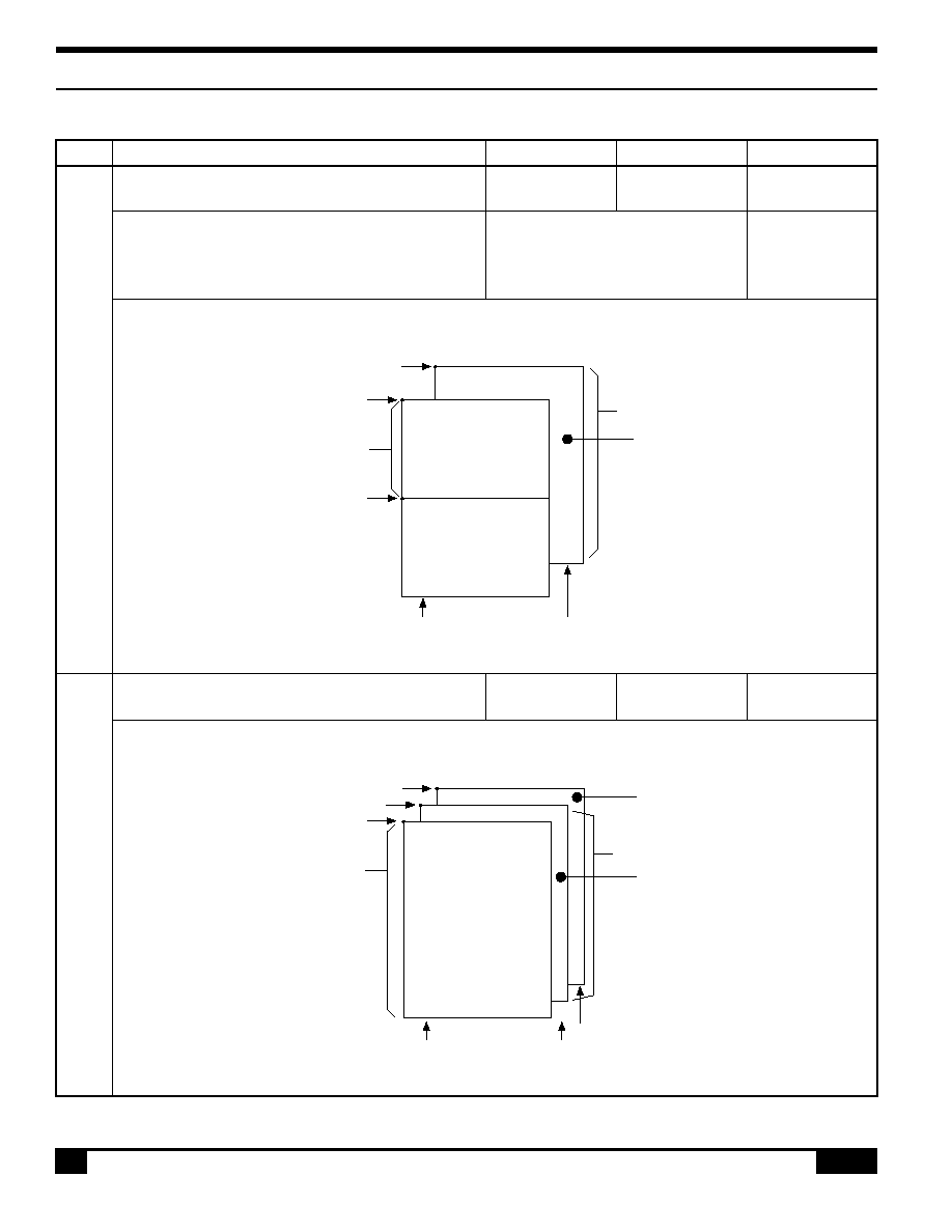
Figure 8. Single-panel display
Figure 9. Dual-panel display
EI
X driver
X driver
LCD
Y driver
YD
EI
X driver
X driver
YD
X driver
X driver
Upper Panel
Lower Panel
Y driver
S-MOS Systems, Inc. · 2460 North First Street · San Jose, CA 95131 · Tel: (408) 922-0200 · Fax: (408) 922-0238
268-0.4
31
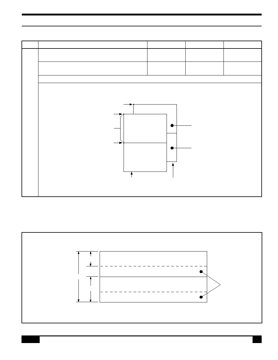
3.2.1.5
3.0 Command Description
EI
YD
Y driver
X driver
X driver
X driver
X driver
Right Panel
Left Panel
Note: There are no Seiko-Epson LCD units in the configuration shown in Figure 10.
Figure 10. Left-and-right two-panel display
Table 3. LCD parameters
Parameter
W/S = 0
W/S = 1
IV = 1
IV = 0
IV = 1
IV = 0
C/R
C/R
C/R
C/R
C/R
TC/R
TC/R
TC/R (see note 1)
TC/R
TC/R
L/F
L/F
L/F
L/F
L/F
SL1
00H to L/F
00H to L/F + 1
(L/F) / 2
(L/F) / 2
(see note 2)
SL2
00H to L/F
00H to L/F + 1
(L/F) / 2
(L/F) / 2
(see note 2)
SAD1
First screen block
First screen block
First screen block
First screen block
SAD2
Second screen block Second screen block Second screen block Second screen block
SAD3
Third screen block
Third screen block
Third screen block
Third screen block
SAD4
Invalid
Invalid
Fourth screen block
Fourth screen block
Cursor move-
Continuous movement over whole screen
Above-and-below configuration:
ment range
continuousmovement over whole screen
Notes:
1. See table 31 (page 105) for further details on setting the C/R and TC/R parameters when using the HDOT SCR command.
2. The value of SL when IV = 0 is equal to the value of SL when IV = 1, plus one.
S-MOS Systems, Inc. · 2460 North First Street · San Jose, CA 95131 · Tel: (408) 922-0200 · Fax: (408) 922-0238
32
268-0.4
3.0 Command Description
3.2.1.6 3.2.1.9
3.2.1.6 IV
Screen origin compensation for inverse display. IV is
usually set to 1.
The best way of displaying inverted characters is to
Exclusive-OR the text layer with the graphics back-
ground layer. However, inverted characters at the top
or left of the screen are difficult to read as the charac-
ter origin is at the top-left of its bitmap and there are no
background pixels either above or to the left of these
characters.
The IV flag causes the SED1330F/1335F/1336F to
offset the text screen against the graphics back layer
by one vertical pixel. Use the horizontal pixel scroll
function (HDOT SCR) to shift the text screen 1 to 7
pixels to the right. All characters will then have the
necessary surrounding background pixels that en-
sure easy reading of the inverted characters.
See Section 5.5 for information on scrolling.
IV = 0:
Screen top-line correction
IV = 1:
No screen top-line correction (no
offset)
3.2.1.7 T/L
Selects TV or LCD mode. When TV mode is selected,
the TV sync generator circuit is ON.
T/L = 0: LCD mode
T/L = 1: TV mode
3.2.1.9 FX
Sets the width, in pixels, of the character field. The
character width in pixels is equal to FX + 1, where FX
can range from 00 to 07H inclusive. If data bit 3 is set
(FX is in the range 08 to 0FH) and an 8-pixel font is
used, a space is inserted between characters. Note
that the maximum character width in TV mode is eight
pixels.
Table 4. Horizontal character size selection
FX
[FX] character width
HEX
D3 D2 D1 D0
(pixels)
00
0
0
0
0
1
01
0
0
0
1
2
07
0
1
1
1
8
Since the SED1330F/1335F/1336F handles display
data in 8-bit units, characters larger than 8 pixels wide
must be formed from 8-pixel segments. As Figure 12
shows, the remainder of the second eight bits are not
displayed. This also applies to the second screen layer.
In graphics mode, the normal character field is also
eight pixels. If a wider character field is used, any
remainder in the second eight bits is not displayed.
3.2.1.8 DR
Selects output of an additional shift-clock cycle for
every 64 pixels. The extra cycles are required for
correct operation of the enable chain when using a
two-panel display.
DR = 0: Normal operation
DR = 1: Additional shift-clock cycles
IV
1 dot
Dots 1 to 7
Display start point
Back layer
HDOT SCR
Character
Figure 11. IV and HDOT SCR adjustment
S-MOS Systems, Inc. · 2460 North First Street · San Jose, CA 95131 · Tel: (408) 922-0200 · Fax: (408) 922-0238
268-0.4
33
3.2.1.10 3.2.1.11
3.0 Command Description
8 bits
FY
FX
8 bits
FY
FX
Non-display area
Address B
Address A
8 bits
8 bits
Figure 12. FX and FY display addresses
3.2.1.10 WF
Selects the AC frame drive waveform period. WF is
usually set to 1.
WF = 0: 16-line AC drive
WF = 1: two-frame AC drive
In two-frame AC drive, the WF period is twice the
frame period.
In 16-line AC drive, WF inverts every 16 lines.
Although 16-line AC drive gives a more readable
display, horizontal lines may appear when using high
LCD drive voltages or at high viewing angles.
3.2.1.11 FY
Sets the height, in pixels, of the character. The height
in pixels is equal to FY + 1.
FY can range from 00 to 0FH inclusive.
Set FY to zero (vertical size equals one) when in
graphics mode.
Table 5. Vertical character size selection
FY
[FY] character
HEX
D3 D2 D1 D0
height (pixels)
00
0
0
0
0
1
01
0
0
0
1
2
07
0
1
1
1
8
0E
1
1
1
0
15
0F
1
1
1
1
16
S-MOS Systems, Inc. · 2460 North First Street · San Jose, CA 95131 · Tel: (408) 922-0200 · Fax: (408) 922-0238
34
268-0.4
3.0 Command Description
3.2.1.12 3.2.1.13
3.2.1.12 C/R
Sets the address range covered by one display line,
that is, the number of characters less one, multiplied
by the number of horizontal bytes per character.
C/R can range from 0 to 239.
For example, if the character width is 10 pixels, then
the address range is equal to twice the number of
characters, less 2. See Section 9.1.1 for the calcula-
tion of C/R.
[C/R] cannot be set to a value greater than the
address range. It can, however, be set smaller than
the address range, in which case the excess display
area is blank. The number of excess pixels must not
exceed 64.
Table 6. Display line address range
C/R
[C/R] bytes per display line
HEX
D7
D6
D5
D4
D3
D2
D1
D0
00
0
0
0
0
0
0
0
0
1
01
0
0
0
0
0
0
0
1
2
4F
0
1
0
0
1
1
1
1
80
EE
1
1
1
0
1
1
1
0
239
EF
1
1
1
0
1
1
1
1
240
3.2.1.13 TC/R
Sets the length, including horizontal blanking, of one
line. The line length is equal to TC/R + 1, where TC/
R can range from 0 to 255.
TC/R must be greater than or equal to C/R + 4.
Provided this condition is satisfied, [TC/R] can be set
according to the equation given in section 9.1.1 in
order to hold the frame period constant and minimize
jitter for any given main oscillator frequency, f
OSC
.
Table 7. Line length selection
TC/R
[TC/R] line length (bytes)
HEX
D7
D6
D5
D4
D3
D2
D1
D0
00
0
0
0
0
0
0
0
0
1
01
0
0
0
0
0
0
0
1
2
52
0
1
0
1
0
0
1
0
83
FE
1
1
1
1
1
1
1
0
255
FF
1
1
1
1
1
1
1
1
256
S-MOS Systems, Inc. · 2460 North First Street · San Jose, CA 95131 · Tel: (408) 922-0200 · Fax: (408) 922-0238
268-0.4
35
3.2.1.14 3.2.1.15
3.0 Command Description
3.2.1.14 L/F
Sets the height, in lines, of a frame. The height in lines
is equal to L/F + 1, where L/F can range from 0 to 255.
If W/S is set to 1, selecting two-screen display, the
number of lines must be even and L/F must, therefore,
be an odd number.
Table 8. Frame height selection
L/F
[L/F] lines per frame
HEX
D7
D6
D5
D4
D3
D2
D1
D0
00
0
0
0
0
0
0
0
0
1
01
0
0
0
0
0
0
0
1
2
7F
0
1
1
1
1
1
1
1
128
FE
1
1
1
1
1
1
1
0
255
FF
1
1
1
1
1
1
1
1
256
Table 9. Frame heights and compatible LCD units
Number of lines [LF]
Panel Duty Cycle
64
1/64
128
1/64
Table 10. Horizontal address range
Hex code
[AP] addresses
APH
APL
per line
0
0
0
0
0
0
0
0
1
1
0
0
5
0
80
F
F
F
E
2
16
2
F
F
F
F
2
16
1
3.2.1.15 AP
Defines the horizontal address range of the virtual
screen. APL is the least significant byte of the ad-
dress.
Figure 13. AP parameters
APL
AP7
AP6
AP5
AP4
AP3
AP2
AP1
AP0
APH
AP15
AP14
AP13
AP12
AP11
AP10
AP9
AP8
S-MOS Systems, Inc. · 2460 North First Street · San Jose, CA 95131 · Tel: (408) 922-0200 · Fax: (408) 922-0238
36
268-0.4
3.0 Command Description
3.2.1.15 3.3.1
Figure 14. AP and C/R relationship
3.2.2 SLEEP IN
Places the system in standby mode. This command
has no parameter bytes. At least one blank frame after
receiving this command, the SED1330F/1335F/1336F
halts all internal operations, including the oscillator,
and enters the sleep mode. Blank data is sent to the
X-drivers, and the Y-drivers have their bias supplies
turned off by the YDIS signal. Using the YDIS signal
to disable the Y-drivers guards against any spurious
displays.
The internal registers of the SED1330F/1335/1336F
maintain their values during the sleep mode. The
display memory control pins maintain their logic levels
to ensure that the display memory is not corrupted.
The SED1330F/1335F/1336F can be removed from
the sleep state by sending the SYSTEM SET com-
mand with only the P1 parameter. The DISP ON
command should be sent next to enable the display.
Figure 15. SLEEP IN instruction
1. The YDIS signal goes LOW between one
and two frames after the SLEEP IN com-
mand is received. Since YDIS forces all
display driver outputs to go to the dese-
lected output voltage, YDIS can be used as
a power-down signal for the LCD unit. This
can be done by having YDIS turn off the
relatively high-power LCD drive supplies at
the same time as it blanks the display.
2. Since all internal clocks in the SED1330F/
1335F/1336F are halted while in the sleep
state, a DC voltage will be applied to the LCD
panel if the LCD drive supplies remain on.
If reliability is a prime consideration, turn off
the LCD drive supplies before issuing the
SLEEP IN command.
3. Note that, although the bus lines become
high impedance in the sleep state, pull-up
or pull-down resistors on the bus line will
force these lines to a known state.
3.3 Display Control Commands
3.3.1 DISP ON/OFF
Turns the whole display on or off. The single-byte
parameter enables and disables the cursor and lay-
ered screens, and sets the cursor and screen flash
rates. The cursor can be set to flash over one charac-
ter or over a whole line.
MSB
LSB
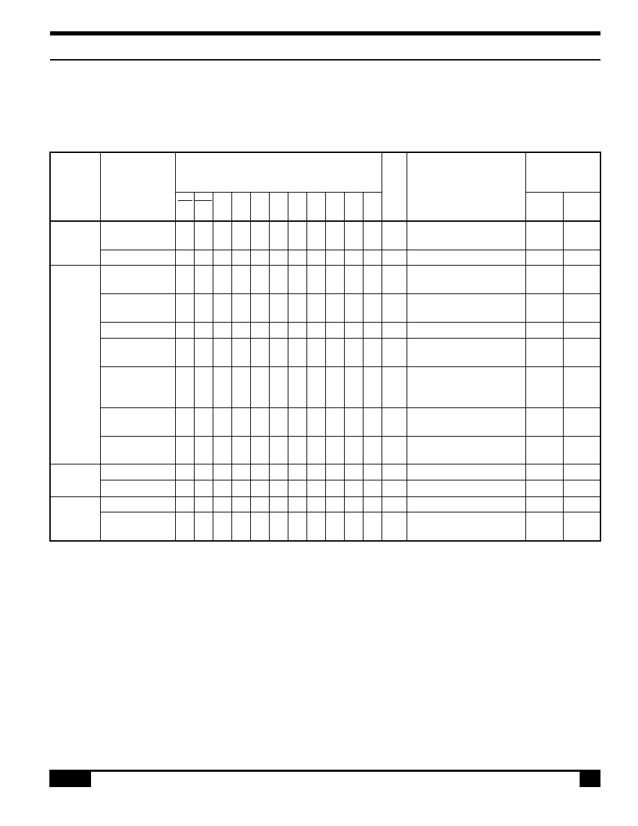
C
0
1
0
1
0
0
1
1
Figure 16. DISP ON/OFF parameters
MSB
LSB
C
0
1
0
1
1
0
0
0
P1
FP5 FP4 FP3 FP2 FP1 FP0 FC1 FC0
Display area
C/R
Display memory limit
AP
S-MOS Systems, Inc. · 2460 North First Street · San Jose, CA 95131 · Tel: (408) 922-0200 · Fax: (408) 922-0238
268-0.4
37
3.3.1.1 3.3.2.1
3.0 Command Description
3.3.1.1 D
Turns the display ON or OFF. The D bit takes prece-
dence over the FP bits in the parameter.
D = 0:
Display OFF
D = 1:
Display ON
3.3.1.2 FC
Enables/disables the cursor and sets the flash rate.
The cursor flashes with a 70% duty cycle (ON/OFF).
Table 11. Cursor flash rate selection
FC1
FC0
Cursor display
0
0
OFF (blank)
0
1
No flashing
1
0
Flash at f
FR
/32 Hz
(approx. 2 Hz)
1
1
Flash at f
FR
/64 Hz
(approx. 1 Hz)
Note: As the MWRITE command always enables the cursor,
the cursor position can be checked even when perform-
ing consecutive writes to display memory while the
cursor is flashing.
3.3.1.3 FP
Each pair of bits in FP sets the attributes of one screen
block, as follows.
Table 12. Screen block attribute selection
FP1
FP0
First screen block (SAD1)
FP3
FP2
Second screen block (SAD2,
SAD4). See note.
FP5
FP4
Third screen block (SAD3)
0
0
OFF (blank)
0
1
No flashing
1
0
Flash at f
FR
/32 Hz
(approx. 2 Hz)
1
1
Flash at f
FR
/4 Hz
(approx. 16 Hz)
Note: If SAD4 is enabled by setting W/S to 1, FP3 and FP2
control both SAD2 and SAD4. The attributes of SAD2
and SAD4 cannot be set independently.
3.3.2 SCROLL
3.3.2.1 C
Sets the scroll start address and the number of lines
per scroll block. Parameters P1 to P10 can be omitted
if not required. The parameters must be entered
sequentially as shown in Figure 17.
ON
ON
MSB
LSB
C
0
1
0
0
0
1
0
0
P1
A7
A6
A5
A4
A3
A2
A1
A0 (SAD 1L)
P2
A15 A14 A13 A12 A11 A10
A9
A8 (SAD 1H)
P3
L7
L6
L5
L4
L3
L2
L1
L0
(SL 1)
P4
A7
A6
A5
A4
A3
A2
A1
A0 (SAD 2 L)
P5
A15 A14 A13 A12 A11 A10
A9
A8 (SAD 2H)
P6
L7
L6
L5
L4
L3
L2
L1
L0
(SL 2)
P7
A7
A6
A5
A4
A3
A2
A1
A0 (SAD 3L)
P8
A15 A14 A13 A12 A11 A10
A9
A8 (SAD 3H)
P9
A7
A6
A5
A4
A3
A2
A1
A0 (SAD 4L)
P10 A15 A14 A13 A12 A11 A10
A9
A8 (SAD 4H)
Note: Set parameters P9 and P10 only if both two-screen
drive (W/S = 1) and two-layer configuration are se-
lected. SAD4 is the fourth screen block display start
address.
Figure 17. SCROLL instruction parameters
S-MOS Systems, Inc. · 2460 North First Street · San Jose, CA 95131 · Tel: (408) 922-0200 · Fax: (408) 922-0238
38
268-0.4
3.0 Command Description
3.3.2.1 3.3.2.2
Table 13. Screen block start address selection
SL1, SL2
[SL] screen lines
HEX
L7
L6
L5
L4
L3
L2
L1
L0
00
0
0
0
0
0
0
0
0
1
01
0
0
0
0
0
0
0
1
2
7F
0
1
1
1
1
1
1
1
128
FE
1
1
1
1
1
1
1
0
255
FF
1
1
1
1
1
1
1
1
256
3.3.2.2 SL1, SL2
SL1 and SL2 set the number of lines per scrolling
screen. The number of lines is SL1 or SL2 plus one.
The relationship between SAD, SL and the display
mode is described below.
Table 14. Text display mode
W/S
Screen
First Layer
Second Layer
First screen block
SAD1
SAD2
Second screen block
SL1
SL2
SAD3 (see note 1)
Third screen block (partitioned screen)
Set both SL1 and SL2 to L/F + 1
if not using a partitioned screen.
Screen configuration example:
0
(continued)
Character display page 1
Character display page 3
SAD2
SAD1
SAD3
SL1
SL2
Graphics display page 2
Layer 2
Layer 1
S-MOS Systems, Inc. · 2460 North First Street · San Jose, CA 95131 · Tel: (408) 922-0200 · Fax: (408) 922-0238
268-0.4
39
3.3.2.2
3.0 Command Description
Table 14. Text display mode (continued)
W/S
Screen
First Layer
Second Layer
Upper screen
SAD1
SAD2
SL1
SL2
Lower screen
SAD3
SAD4
(see note 2)
(see note 2)
Set both SL1 and SL2 to ((L/F) / 2 + 1)
Screen configuration example:
1
Notes:
1. SAD3 has the same value as either SAD1 or SAD2, whichever has the least number of lines (set by SL1 and SL2).
2. Since the parameters corresponding to SL3 and SL4 are fixed by L/F, they do not have to be set in this mode.
Character display page 1
Character display page 3
SAD2
SAD1
SAD3
SL1
Graphics display page 2
Layer 2
Layer 1
Graphics display page 4
(SAD4)
S-MOS Systems, Inc. · 2460 North First Street · San Jose, CA 95131 · Tel: (408) 922-0200 · Fax: (408) 922-0238
40
268-0.4
3.0 Command Description
3.3.2.2
Table 15. Graphics display mode
W/S
Screen
First Layer
Second Layer
Third Layer
Two-layer composition
SAD1
SAD2
SL1
SL2
SAD3 (see note 3)
Upper screen
Set both SL1 and SL2 to
L/F + 1 if not using a
partitioned screen
Screen configuration example:
0
0
Three-layer configuration
SAD1
SAD2
SAD3
SL1 = L/F + 1
SL2 = L/F + 1
--
Screen configuration example:
Character display page 1
Character display page 3
SAD2
SAD1
SAD3
SL1
SL2
Graphics display page 2
Layer 1
Layer 2
Graphics display page 1
SAD2
SAD1
SAD3
SL1
SL2
Graphics display page 2
Layer 1
Graphics display page 3
Layer 2
Layer 3
S-MOS Systems, Inc. · 2460 North First Street · San Jose, CA 95131 · Tel: (408) 922-0200 · Fax: (408) 922-0238
268-0.4
41
3.3.2.2
3.0 Command Description
Notes:
1. SAD3 has the same value as either SAD1 or SAD2, whichever has the least number of lines (set by SL1 and SL2).
2. Since the parameters corresponding to SL3 and SL4 are fixed by L/F, they do not have to be set.
3. If, and only if, W/S = 1, the differences between SL1 and (L/F + 1) / 2, and between SL2 and (L/F + 1) / 2, are blanked.
Table 15. Graphics display mode (continued)
W/S
Screen
First Layer
Second Layer
Third Layer
Upper screen
SAD1
SAD2
--
SL1
SL2
Lower screen
SAD3
SAD4
--
(see note 2)
(see note 2)
Set both SL1 and SL2 to ((L/F) / 2 + 1)
Screen configuration example (see note 3):
1
Figure 18. Two-panel display height
Graphics display page 1
Graphics display page 3
SAD2
SAD1
SAD3
SL1
Graphics display page 2
Layer 2
Layer 1
Graphics display page 4
Upper Panel
Lower Panel
SL1
L/2
L
Graphics
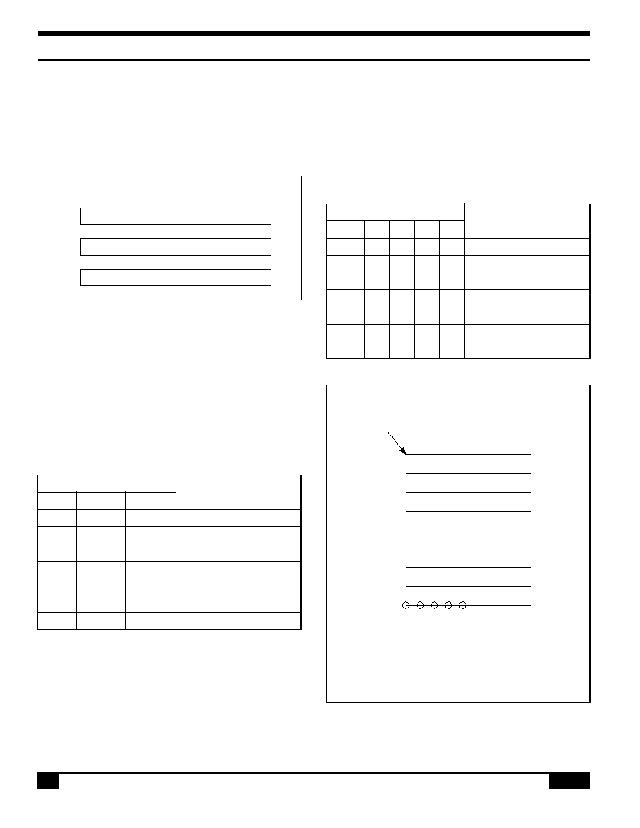
S-MOS Systems, Inc. · 2460 North First Street · San Jose, CA 95131 · Tel: (408) 922-0200 · Fax: (408) 922-0238
42
268-0.4
MSB
LSB
C
0
1
0
1
1
1
0
1
P1
0
0
0
0
X3
X2
CRX
X1
X0
P2
CM
0
0
0
Y3
Y2
CRY
Y1
Y0
3.0 Command Description
3.3.3 3.3.3.2
3.3.3 CSRFORM
Sets the cursor size and display mode. Although the
cursor is normally only used in text displays, it may
also be used in graphics displays when displaying
special characters.
3.3.3.2 CRY
Sets the location of an underscored cursor in lines,
from the character origin. When using a block cursor,
CRY sets the vertical size of the cursor from the
character origin. CRY is equal to the number of lines
less one.
Table 17. Cursor height selection
CRY
[CRY] cursor
HEX
Y3
Y2
Y1
Y0
height (lines)
0
0
0
0
0
illegal
1
0
0
0
1
2
8
1
0
0
0
9
E
1
1
1
0
15
F
1
1
1
1
16
Figure 20. Cursor size and position
Figure 19. CSRFORM parameter bytes
3.3.3.1 CRX
Sets the horizontal size of the cursor from the charac-
ter origin. CRX is equal to the cursor size less one.
CRX must be less than or equal to FX.
Table 16. Horizontal cursor size selection
CRX
[CRX] cursor width
HEX
X3 X2
X1
X0
(pixels)
0
0
0
0
0
1
1
0
0
0
1
2
8
1
0
0
0
9
E
1
1
1
0
15
F
1
1
1
1
16
0 1 2 3 4 5 6 ·
·
·
0
1
2
3
4
5
6
7
8
9
Character start point
CRX = 5 dots
CRY = 9 dots
CM = 0
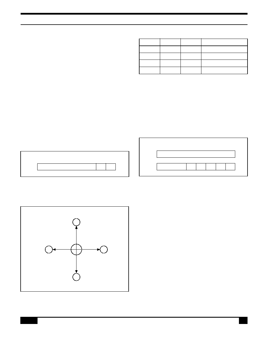
S-MOS Systems, Inc. · 2460 North First Street · San Jose, CA 95131 · Tel: (408) 922-0200 · Fax: (408) 922-0238
268-0.4
43
3.3.3.3 3.3.5.1
3.0 Command Description
3.3.3.3 CM
Sets the cursor display mode. Always set CM to 1
when in graphics mode.
CM = 0: Underline cursor
CM = 1: Block cursor
3.3.4 CSRDIR
Sets the direction of automatic cursor increment. The
cursor can move left or right one character, or up or
down by the number of bytes specified by the address
pitch, AP.
When reading from and writing to display memory,
this automatic cursor increment controls the display
memory address increment on each read or write.
Table 18. Cursor shift direction
C
CD1
CD0
Shift direction
4CH
0
0
Right
4DH
0
1
Left
4EH
1
0
Up
4FH
1
1
Down
Note: Since the cursor moves in address units even if FX
9,
the cursor address increment must be preset for move-
ment in character units. See Section 5.3.
3.3.5 OVLAY
Selects layered screen composition and screen text/
graphics mode.
MSB
LSB
C
0
1
0
0
1
1
CD1 CD2
Figure 21. CSRDIR parameters
Figure 22. Cursor direction
MSB
LSB
C
0
1
0
1
1
0
1
1
P1
0
0
0
OV DM2 DM1 MX1 MX0
Figure 23. OVLAY parameter
3.3.5.1 MX0, MX1
MX0 and MX1 set the layered screen composition
method, which can be either OR, AND, Exclusive-OR
or Priority-OR. Since the screen composition is orga-
nized in layers and not by screen blocks, when using
a layer divided into two screen blocks, different com-
position methods cannot be specified for the indi-
vidual screen blocks.
The Priority-OR mode is the same as the OR mode
unless flashing of individual screens is used.
10
11
00
01
1
+1
+AP
AP
S-MOS Systems, Inc. · 2460 North First Street · San Jose, CA 95131 · Tel: (408) 922-0200 · Fax: (408) 922-0238
44
268-0.4
3.0 Command Description
3.3.5.1
Table 19. Composition method selection
MX1
MX0
Function
Composition Method
Applications
0
0
L1
L2
L3
OR
Underlining, rules, mixed text and graphics
0
1
(L1
L2)
L3
Exclusive-OR
Inverted characters, flashing regions, un-
derlining
1
0
(L1
L2)
L3
AND
Simple animation, three-dimensional ap-
1
1
L1 > L2 > L3
Priority-OR
pearance
Notes:
L1: First layer (text or graphics). If text is selected, layer L3 cannot be used.
L2: Second layer (graphics only)
L3: Third layer (graphics only)
Notes:
L1: Not flashing
L2: Flashing at 1 Hz
L3: Flashing at 2 Hz
Figure 24. Combined layer display
EPSON
Layer 1
Layer 2
Layer 3
EPSON
Visible display
1
OR
EPSON
EPSON
2
Exclusive OR
EPSON
3
AND
EPSON
4
Prioritized OR
EPSON
SON
S-MOS Systems, Inc. · 2460 North First Street · San Jose, CA 95131 · Tel: (408) 922-0200 · Fax: (408) 922-0238
268-0.4
45
3.3.5.2 3.3.7.1
3.0 Command Description
3.3.5.2 DM1, DM2
DM1 and DM2 specify the display mode of screen
blocks 1 and 3, respectively.
DM1/2 = 0: Text mode
DM1/2 = 1: Graphics mode
Note 1: Screen blocks 2 and 4 can only display graphics.
Note 2: DM1 and DM2 must be the same, regardless of the
setting of W/S.
3.3.5.3 OV
Specifies two- or three-layer composition in graphics
mode.
OV = 0: Two-layer composition
OV = 1: Three-layer composition
Set OV to 0 for mixed text and graphics mode.
3.3.6 CGRAM ADR
Specifies the CG RAM start address.
MSB
LSB
C
0
1
0
1
1
1
0
0
P1
A7
A6
A5
A4
A3
A2
A1
A0 (SAGL)
P2
A15 A14 A13 A12 A11 A10
A9
A8 (SAGH)
Figure 25. CGRAM ADR parameters
Note: See Section 6 for information on the SAG parameters.
3.3.7 HDOT SCR
While the scroll command only allows scrolling by
characters, HDOT SCR allows the screen to be scrolled
horizontally by pixels. HDOT SCR cannot be used on
individual layers.
MSB
LSB
C
0
1
0
1
1
0
1
0
P1
0
0
0
0
0
D2
D1
D0
3.3.7.1 D0 to D2
Specifies the number of pixels to scroll. The C/R
parameter has to be set to one more than the number
of horizontal characters before using HDOT SCR.
Smooth scrolling can be simulated if the controlling
microprocessor repeatedly issues the HDOT SCR
command to the SED1330F/1335F/1336F. See Sec-
tion 5.5 for more information on scrolling the display.
Table 20. Scroll step selection
P1
Number of pixels
HEX
D2 D1 D0
to scroll
00
0
0
0
0
01
0
0
1
1
02
0
1
0
2
06
1
1
0
6
07
1
1
1
7
Figure 26. HDOT SCR parameters
S-MOS Systems, Inc. · 2460 North First Street · San Jose, CA 95131 · Tel: (408) 922-0200 · Fax: (408) 922-0238
46
268-0.4
3.0 Command Description
3.4 3.4.2
3.4 Drawing Control Commands
3.4.1 CSRW
The 16-bit cursor address register contains the dis-
play memory of the data at the cursor position as
shown in Figure 28.
Figure 28. CSRW parameters
Note that the microprocessor cannot directly access
the display memory.
The MREAD and MWRITE commands use the ad-
dress in this register.
The cursor address register can only be modified by
the CSRW command, and by the automatic incre-
ment after an MREAD or MWRITE command. It is not
affected by display scrolling.
If a new address is not set, display memory accesses
will be from the last set address or the address after
previous automatic increments.
3.4.2 CSRR
Reads from the cursor address register. After issuing
the command, the data read address is read twice, for
the low byte and then the high byte of the register.
MSB
LSB
C
0
1
0
0
0
1
1
0
P1
A7
A6
A5
A4
A3
A2
A1
A0 (CSRL)
P2
A15 A14 A13 A12 A11 A10
A9
A8 (CSRH)
Figure 29. CSRR parameters
MSB
LSB
C
0
1
0
0
0
1
1
1
P1
A7
A6
A5
A4
A3
A2
A1
A0 (CSRL)
P2
A15 A14 A13 A12 A11 A10
A9
A8 (CSRH)
M
A
B
X
Y
A
B
X
Y
Z
A
B
X
Y
Z
M = 0
N = 0
Display width
N
M/N is the number of bits (dots) that parameter 1 (P1)
is incremented/decremented by.
Figure 27. Horizontal scrolling
S-MOS Systems, Inc. · 2460 North First Street · San Jose, CA 95131 · Tel: (408) 922-0200 · Fax: (408) 922-0238
268-0.4
47
3.5 3.5.2
3.0 Command Description
3.5 Memory Control Commands
3.5.1 MWRITE
The microprocessor may write a sequence of data
bytes to display memory by issuing the MREAD
command and then writing the bytes to the SED1330F/
1335F/1336F. There is no need for further MWRITE
commands or for the microprocessor to update the
cursor address register after each byte as the cursor
address is automatically incremented by the amount set
with CSRDIR, in preparation for the next data write.
Figure 30. MWRITE parameters
3.5.2 MREAD
Puts the SED1330F/1335F/1336F into the data out-
put state. On the MREAD command, the display
memory data at the cursor address is read into a
buffer in the SED1330F/1335F/1336F.
Each time the microprocessor reads the buffer, the
cursor address is incremented by the amount set by
CSRDIR and the next data byte fetched from memory,
so a sequence of data bytes may be read without
further MREAD commands or by updating the cursor
address register.
If the cursor is displayed, the read data will be from two
positions ahead of the cursor.
Figure 31. MREAD parameters
MSB
LSB
C
0
1
0
0
0
0
1
0
P1
P2
Pn
n
1
Note:
P1, P2, ..., Pn: display data.
MSB
LSB
C
0
1
0
0
0
0
1
1
P1
P2
Pn
n
1

S-MOS Systems, Inc. · 2460 North First Street · San Jose, CA 95131 · Tel: (408) 922-0200 · Fax: (408) 922-0238
48
268-0.4
1.0 Overview
1.3
THIS PAGE INTENTIONALLY BLANK

S-MOS Systems, Inc. · 2460 North First Street · San Jose, CA 95131 · Tel: (408) 922-0200 · Fax: (408) 922-0238
268-0.4
49
3.3.2.2
3.0 Command Description
4.0
Specifications

S-MOS Systems, Inc. · 2460 North First Street · San Jose, CA 95131 · Tel: (408) 922-0200 · Fax: (408) 922-0238
50
268-0.4
THIS PAGE INTENTIONALLY BLANK
S-MOS Systems, Inc. · 2460 North First Street · San Jose, CA 95131 · Tel: (408) 922-0200 · Fax: (408) 922-0238
268-0.4
51
4.0 4.1
4.0 Specifications
4.0 Specifications
4.1 Absolute Maximum Ratings
4.1.1 SED1330
Parameter
Symbol
Rating
Unit
Supply voltage range
V
DD
0.3 to 7.0
V
Input voltage range
V
IN
0.5 to V
DD
+ 0.5
V
Power dissipation
P
D
300
mW
Operating temperature range
T
opr
20 to 75
°
C
Storage temperature range
T
stg
65 to 150
°
C
Soldering temperature (10 seconds). See note 1.
T
solder
260
°
C
4.1.2 SED1335/SED1336
Parameter
Symbol
Rating
Unit
Supply voltage range
V
DD
0.3 to 7.0
V
Input voltage range
V
IN
0.3 to V
DD
+ 0.3
V
Power dissipation
P
D
300
mW
Operating temperature range
T
opr
20 to 75
°
C
Storage temperature range
T
stg
65 to 150
°
C
Soldering temperature (10 seconds). See note 1.
T
solder
260
°
C
Notes:
1. The humidity resistance of the flat package may be reduced if the package is immersed in solder. Use a soldering technique
that does not heatstress the package.
2. If the power supply has a high impedance, a large voltage differential can occur between the input and supply voltages. Take
appropriate care with the power supply and the layout of the supply lines. (See Section 2.3.)
3. All supply voltages are referenced to V
SS
= 0V.
S-MOS Systems, Inc. · 2460 North First Street · San Jose, CA 95131 · Tel: (408) 922-0200 · Fax: (408) 922-0238
52
268-0.4
4.0 Specifications
4.2
V
DD
= 5V
±
10%, V
SS
= 0V, T
a
= 20 to 75
°
C
Measured at OSC1
4.2 SED 1330 Electrical Characteristics
Parameter
Symbol
Condition
Rating
Unit
min
typ
max
Supply voltage
V
DD
4.5
5.0
5.5
V
Register data retention voltage
V
OH
2.0
--
5.5
V
Input leakage current
I
LI
V
I
= V
DD
.
--
0.05
2.0
µ
A
Output leakage current
I
LO
V
I
= V
SS
.
--
0.10
5.0
µ
A
Operating supply current
I
opr
See note 4.
--
8
12
mA
Quiescent supply current
I
Q
V
OSC1
= V
CS
= V
RD
= V
DD
--
0.05
20.0
µ
A
Oscillator frequency
f
OSC
1.0
--
10.0
MHz
External clock frequency
f
CL
--
--
10.0
MHz
Oscillator feedback resistance
R
f
0.5
1.0
5.0
M
TTL
HIGH-level input voltage
V
IHT
See note 1.
2.2
--
V
DD + 0.3
V
LOW-level input voltage
V
ILT
See note 1.
0.3
--
0.8
V
HIGH-level output voltage
V
OHT
I
OH
= 5.0 mA.
2.4
--
--
V
See note 1.
LOW-level output voltage
V
OLT
I
OL
= 5.0 mA. See note 1.
--
--
0.4
V
CMOS
HIGH-level input voltage
V
IHC
See note 2.
0.8V
DD
--
--
V
LOW-level input voltage
V
ILC
See note 2.
--
--
0.2V
DD
V
HIGH-level output voltage
V
OHC
I
OH
= 1.6 mA. See note 2.
V
DD
0.4
--
--
V
LOW-level output voltage
V
OLC
I
OH
= 1.6 mA. See note 2.
--
--
0.4
V
Schmitt-trigger
Rising-edge threshold voltage
V
T+
See note 3.
0.5V
DD
0.7V
DD
0.8V
DD
V
Falling-edge threshold voltage
V
T
See note 3.
0.2V
DD
0.3V
DD
0.5V
DD
V
Notes:
1. D0 to D7, A0, CS, RD, WR, VD0 to VD7, VA0 to VA15,
VR/W and VCE are TTL-level inputs.
2. SEL1, SEL2 and OSC1 are CMOS-level inputs. YD,
XD0 to XD3, XSCL, YECL, LP, WF, YSCL, YDIS and
CLO are CMOS-level outputs.
3. RES is a Schmitt-trigger input. The pulsewidth on RES
must be at least 200
µ
s. Note that pulses of more than
a few seconds will cause DC voltages to be applied to
the LCD panel.
4. f
OSC
= 10 MHz, no load (no display memory), internal
character generator, 256
×
200 pixel display. The
operating supply current can be reduced by approxi-
mately 1 mA by setting both CLO and the display OFF.
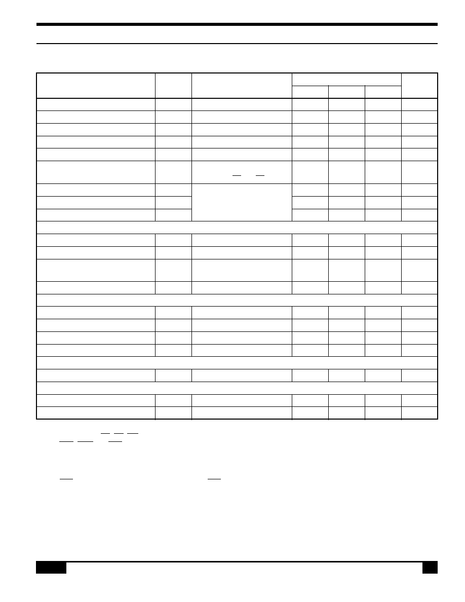
S-MOS Systems, Inc. · 2460 North First Street · San Jose, CA 95131 · Tel: (408) 922-0200 · Fax: (408) 922-0238
268-0.4
53
Notes:
1. D0 to D7, A0, CS, RD, WR, VD0 to VD7, VA0 to VA15,
VRD, VWR and VCE are TTL-level inputs.
2. SEL1 and NT/PL are CMOS-level inputs. YD, XD0 to
XD3, XSCL, XECL, LP, WF, YSCL, YDIS and CLO are
CMOS-level outputs.
3. RES is a Schmitt-trigger input. The pulsewidth on RES
must be at least 200
µ
s. Note that pulses of more than
a few seconds will cause DC voltages to be applied to
the LCD panel.
4. f
OSC
= 10 MHz, no load (no display memory), internal
character generator, 256
×
200 pixel display. The
operating supply current can be reduced by approxi-
mately 1 mA by setting both CLO and the display OFF.
4.3 SED1335/1336 Electrical Characteristics
Parameter
Symbol
Condition
Rating
Unit
min
typ
max
Supply voltage
V
DD
4.5
5.0
5.5
V
Register data retention voltage
V
OH
2.0
--
6.0
V
Input leakage current
I
LI
V
I
= V
DD
. See note 6.
--
0.05
2.0
µ
A
Output leakage current
I
LO
V
I
= V
SS
. See note 6.
--
0.10
5.0
µ
A
Operating supply current
I
opr
See note 4.
--
11
15
mA
Quiescent supply current
I
Q
Sleep mode,
--
0.05
20.0
µ
A
V
OSC1
= V
CS
= V
RD
= V
DD
Oscillator frequency
f
OSC
1.0
--
10.0
MHz
External clock frequency
f
CL
1.0
--
10.0
MHz
Oscillator feedback resistance
R
f
0.5
1.0
3.0
M
TTL
HIGH-level input voltage
V
IHT
See note 1.
0.5V
DD
--
V
DD
V
LOW-level input voltage
V
ILT
See note 1.
V
SS
--
0.2V
DD
V
HIGH-level output voltage
V
OHT
I
OH
= 5.0 mA.
2.4
--
--
V
See note 1.
LOW-level output voltage
V
OLT
I
OL
= 5.0 mA. See note 1.
--
--
V
SS
+ 0.4
V
CMOS
HIGH-level input voltage
V
IHC
See note 2.
0.8V
DD
--
V
DD
V
LOW-level input voltage
V
ILC
See note 2.
V
SS
--
0.2V
DD
V
HIGH-level output voltage
V
OHC
I
OH
= 2.0 mA. See note 2.
V
DD
0.4
--
--
V
LOW-level output voltage
V
OLC
I
OH
= 1.6 mA. See note 2.
--
--
V
SS
+ 0.4
V
Open-drain
LOW-level output voltage
V
OLN
I
OL
= 6.0 mA. See note 5.
--
--
V
SS
+ 0.4
V
Schmitt-trigger
Rising-edge threshold voltage
V
T+
See note 3.
0.5V
DD
0.7V
DD
0.8V
DD
V
Falling-edge threshold voltage
V
T
See note 3.
0.2V
DD
0.3V
DD
0.5V
DD
V
V
DD
= 4.5 to 5.5V, V
SS
= 0V, T
a
= 20 to 75
°
C
Measured at crystal,
47.5% duty cycle.
See note 7.
4.3
4.0 Specifications
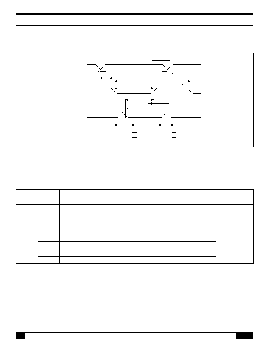
S-MOS Systems, Inc. · 2460 North First Street · San Jose, CA 95131 · Tel: (408) 922-0200 · Fax: (408) 922-0238
54
268-0.4
4.4 SED1330 Timing Diagrams
4.4.1 System bus READ/WRITE timing I (8080)
Figure 32. System bus READ/WRITE timing I (8080)
T
a
= 20 to 75
°
C
4.0 Specifications
4.4 4.4.1
t
ACC8
t
OH8
t
AH8
t
AW8
t
DS8
t
DH8
t
CC
t
CYC
A0, CS
WR, RD
D0~D7
(WRITE)
D0~D7
(READ)
4.4.1.1 SED1330F
Signal
Symbol
Parameter
Rating
Unit
Condition
min
max
A0, CS
t
AH8
Address hold time
10
--
ns
t
AW8
Address setup time
30
--
ns
WR, RD
t
CYC
System cycle time
(1)
--
ns
t
CC
Strobe pulsewidth
220
--
ns
CL = 100
t
DS8
Data setup time
120
--
ns
pF
D0 to D7
t
DH8
Data hold time
10
--
ns
t
ACC8
RD access time
--
120
ns
t
OH8
Output disable time
10
50
ns
Note: t
CYC
= 2t
C
+ t
CC
+ t
CEA
+ 75 > t
ACV
+ 245:
memory control/movement control commands:
= 4t
C
+ t
CC
+ 30:
all other commands:
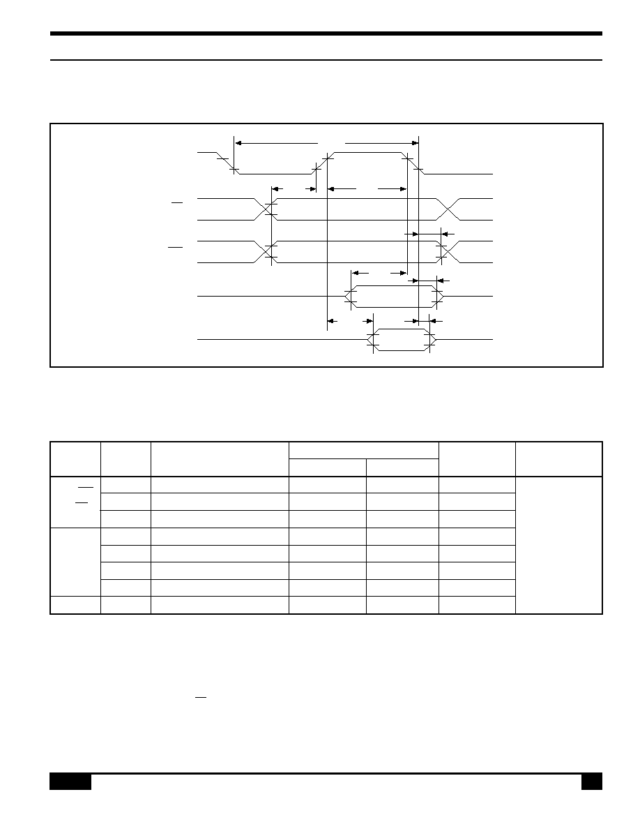
S-MOS Systems, Inc. · 2460 North First Street · San Jose, CA 95131 · Tel: (408) 922-0200 · Fax: (408) 922-0238
268-0.4
55
4.4.2 4.4.2.1
4.0 Specifications
4.4 SED1330 Timing Diagrams
4.4.2 System bus READ/WRITE timing II (6800)
T
a
= 20 to 75
°
C
Figure 33. System bus READ/WRITE timing II (6800)
t
DS6
t
EW
t
AW6
t
AH6
t
DH6
t
OH6
t
ACC6
t
CYC6
E
R/W
A0, CS
D0~D7
(WRITE)
D0~D7
(READ)
4.4.2.1 SED1330F
Signal
Symbol
Parameter
Rating
Unit
Condition
min
max
A0, CS
t
AH6
Address hold time
10
--
ns
R/W
t
AW6
Address setup time
30
--
ns
t
CYC6
System cycle time
(1)
--
ns
CL=100pF+1TTL
t
DS6
Data setup time
120
--
ns
pF
D0 to D7
t
DH6
Data hold time
10
--
ns
t
ACC6
Access time
--
120
ns
t
OH6
Output disable time
10
50
ns
E
t
EW
Enable pulse width
220
--
ns
Note: (1) t
CYC6
= 2t
C
+ t
EW
+ t
CEA
+ 75 > t
ACV
+ 245:
memory control/movement control commands:
= 4t
C
+ t
EW
+ 30:
all other commands:
1.
t
CYC6 means a cycle of (CS.E) not E alone.
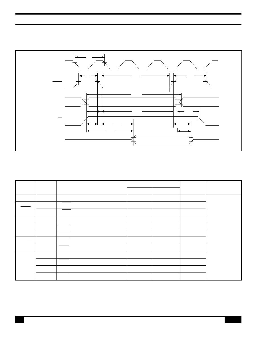
S-MOS Systems, Inc. · 2460 North First Street · San Jose, CA 95131 · Tel: (408) 922-0200 · Fax: (408) 922-0238
56
268-0.4
4.0 Specifications
4.4.3 4.4.3.1
4.4 SED1330 Timing Diagrams
4.4.3 Display memory READ timing
T
a
= 20 to 75
°
C
Figure 34. Display memory READ timing
t
C
t
CE
t
AHC
t
RCH
t
ASC
t
RCS
t
CE3
t
OH2
t
CEA
t
ACY
t
CYR
t
W
t
W
EXT
O
VCE
VA0~VA15
VR/W
VD0~VD7
4.4.3.1 SED1330F
Signal
Symbol
Parameter
Rating
Unit
Condition
min
max
EXT
Ø
0
t
C
Clock cycle
100
--
ns
VCE
t
W
VCE high level pulse width
tc40
--
ns
t
CE
VCE low level pulse width
2tc40
--
ns
VA0
t
CYR
Read cycle time
(1)
--
ns
to VA15
t
ASC
VCE address setup time (fall)
tc45
--
ns
CL = 100pF
t
AHC
VCE address hold time (fall)
2tc40
--
ns
+1TTL
VR/W
t
RCS
VCE read cycle setup time (fall)
tc45
--
ns
t
RCH
VCE read cycle hold time (fall)
tc/235
--
ns
t
ACV
Address access time
--
(2)
ns
VD0
t
CEA
VCE access time
--
(3)
ns
to VD7
t
OH2
Output data hold time
0
--
ns
t
CE2
VCE data off time
0
--
ns
Note: 1.
t
CYR
= 3t
C
2.
t
ACV
= 3t
C
120
3.
t
CEA
= 2t
C
120
S-MOS Systems, Inc. · 2460 North First Street · San Jose, CA 95131 · Tel: (408) 922-0200 · Fax: (408) 922-0238
268-0.4
57
4.4 SED1330 Timing Diagrams
4.4.4 Display memory WRITE timing
T
a
= 20 to 75
°
C
Figure 35. Display memory WRITE timing
4.4.4.1 SED1330F
Signal
Symbol
Parameter
Rating
Unit
Condition
min
max
EXT
Ø
0
t
C
Clock cycle
100
--
ns
VCE
t
W
VCE high level pulse width
tc40
--
ns
t
CE
VCE low level pulse width
2tc40
--
ns
t
CYW
Write cycle time
3tc
--
ns
t
AHC
VCE address hold time (fall)
2tc40
--
ns
VA0
t
ASC
VCE address setup time (fall)
tc55
--
ns
CL = 100pF
to VA15
t
CA
VCE address hold time (rise)
5
--
ns
+1TTL
t
AS
VR/W address setup time (fall)
0
--
ns
t
AH2
VR/W address hold time (rise)
15
--
ns
VR/W
t
WSC
VCE write setup time (fall)
tc55
--
ns
t
WHC
VCE write hold time (fall)
tc240
--
ns
VD0
t
DSC
VCE data input setup time (fall)
twsc10
--
ns
to VD7
t
DHC
VCE data input hold time (fall)
2tc30
--
ns
t
DH2
VR/W data hold time (rise)
10*
50
ns
* Lines VD0 to VD7 are latched.
4.4.4 4.4.4.1
4.0 Specifications
t
WSC
t
C
t
CE
t
CYW
t
AH2
t
CA
t
OH2
t
ASC
t
WHC
t
AS
t
OHC
t
OSC
t
AHC
t
W
EXT
O
VCE
VA0~VA15
VWR
VD0~VD7
S-MOS Systems, Inc. · 2460 North First Street · San Jose, CA 95131 · Tel: (408) 922-0200 · Fax: (408) 922-0238
58
268-0.4
4.4 SED1330 Timing Diagrams
4.4.5 LCD control timing
4.0 Specifications
4.4.5
t
WX
t
DS
t
L1
t
LD
t
WY
t
DHY
t
L2
t
WL
t
DH
t
WXE
t
CX
t
r
t
f
1 frame period
1 line period
ROW1
ROW2
ROW64
t
S2
t
S1
t
Df
ROW NO
LP
YD
WF
YSCL
WF
YSCL
LP
XSCL
XD0~XD3
XECL
XSCL
XD0~XD3
LP
XECL
WF(B)
YD
YSCL
Figure 36. LCD control timing
S-MOS Systems, Inc. · 2460 North First Street · San Jose, CA 95131 · Tel: (408) 922-0200 · Fax: (408) 922-0238
268-0.4
59
4.4 SED1330 Timing Diagrams
4.4.5.1 SED1330F
4.4.5.1
4.0 Specifications
T
a
= 20 to 75
°
C
Signal
Symbol
Parameter
Rating
Unit
Condition
min
max
EXT
Ø
0
t
C
Clock cycle
100
--
ns
t
r
VCE high level pulse width
--
35
ns
t
f
VCE low level pulse width
--
35
ns
XSCL
t
CX
Shift clock cycle time
4tc
--
ns
t
WX
XSCL clock pulse width
t
CX280
--
ns
XD0
t
DH
X-data hold time
t
CX2100
--
ns
V
DD
= 5.0V
to XD3
t
DS
X-data setup time
t
CX2100
--
ns
±
10%
LP
t
LS
Latch data setup time
t
CX2100
--
ns
CL=150F
t
WL
LP signal pulse width
t
CX480
--
ns
t
L1
XECL setup time
t
CX3100
--
ns
t
L2
XECL data hold time
t
C30
--
ns
XECL
t
S1
Enable setup time
t
C30
--
ns
t
S1
Enable delay time
t
C30
--
ns
t
WXE
XECL clock pulse width
t
CX380
--
ns
WF
t
DF
Time allowance of WF delay
--
100
ns
YSCL
t
LD
LP delay time against YSCL
t
CX4100
--
ns
t
WY
YSCL clock pulse width
t
CX480
--
ns
YD
t
DHY
Y-data hold time
t
CX6100
--
ns
S-MOS Systems, Inc. · 2460 North First Street · San Jose, CA 95131 · Tel: (408) 922-0200 · Fax: (408) 922-0238
60
268-0.4
4.4 SED1330 Timing Diagrams
4.4.6 Oscillator timing
T
a
= 20 to 75
°
C
4.0 Specifications
4.4 .6 4.4.6.1
Figure 37. Oscillator timing
t
CL
t
RCL
t
FCL
Sleep period
Power ON
t
WL
t
OSP
t
WH
t
OSS
V
DD
CLO
YDIS
EXT 0O
4.4.6.1 SED1330F
Signal
Symbol
Parameter
Rating
Unit
Condition
min
max
CLO
t
OSP
Time to stable CLO output after power ON
--
3
ms
RES = H
t
OSS
Time to stable CLO output after sleep OFF
--
1
ms
20 pF
t
RCL
External clock rise time
--
15
ns
t
FCL
External clock fall time
--
15
ns
EXTø0
t
WH
External clock high-pulse width
Note 1
Note 2
ns
t
WL
External clock low-pulse width
Note 1
Note 2
ns
t
CL
External clock cycle
100
--
ns
1. (t
C
t
RCL
t
FCL
) X 475/1000 < t
WH
, t
WL
2. (t
C
t
RCL
t
FCL
) X 525/1000 > t
WH
, t
WL
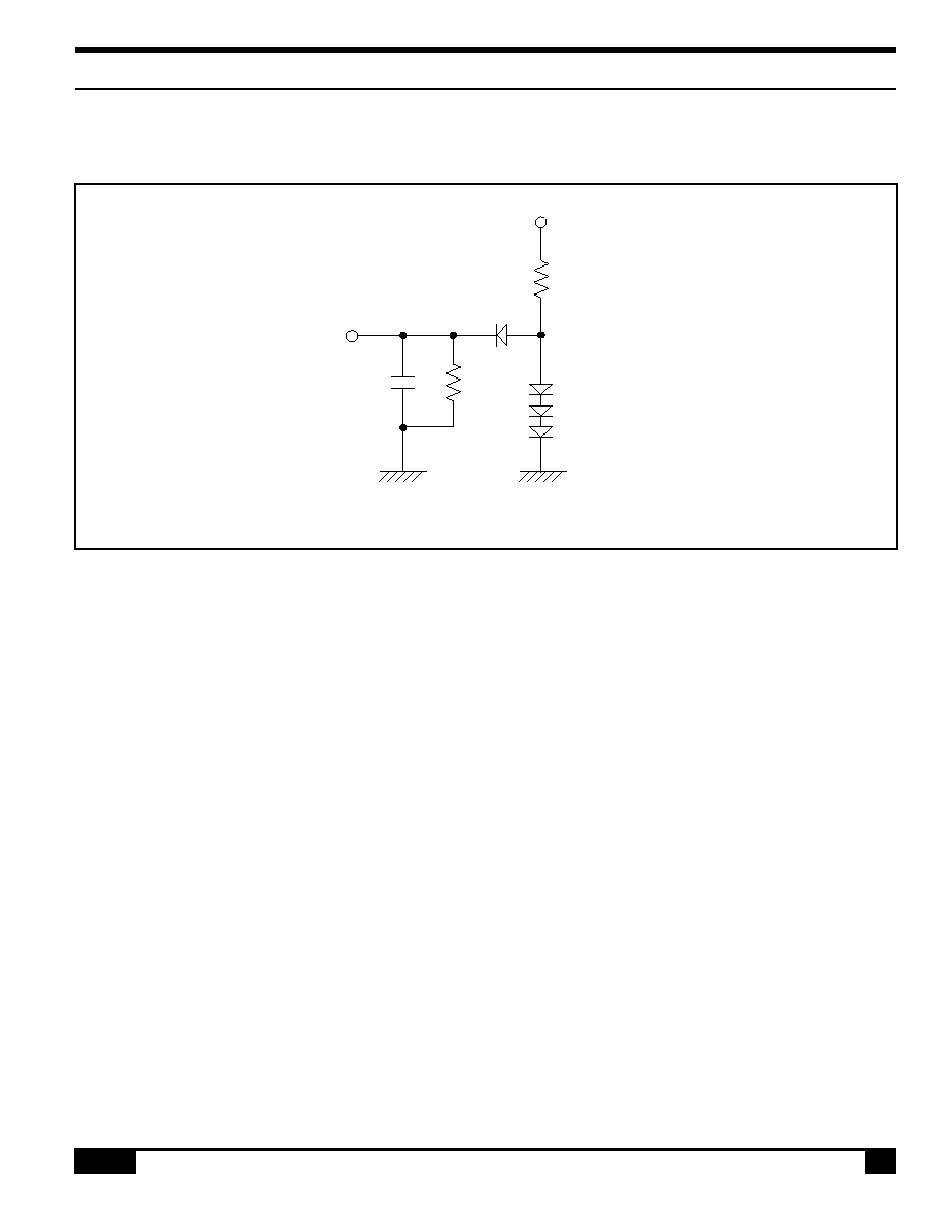
S-MOS Systems, Inc. · 2460 North First Street · San Jose, CA 95131 · Tel: (408) 922-0200 · Fax: (408) 922-0238
268-0.4
61
4.4.7
4.0 Specifications
4.4 SED1330 Timing Diagrams
4.4.7 Measurement circuit
Figure 38. Measurement circuit
C = 100 pF
24 K
2.1 K
IN 916
COMPATABLE
Measurement
Terminal
* C includes probe capacitance.
V
SS
V
DD
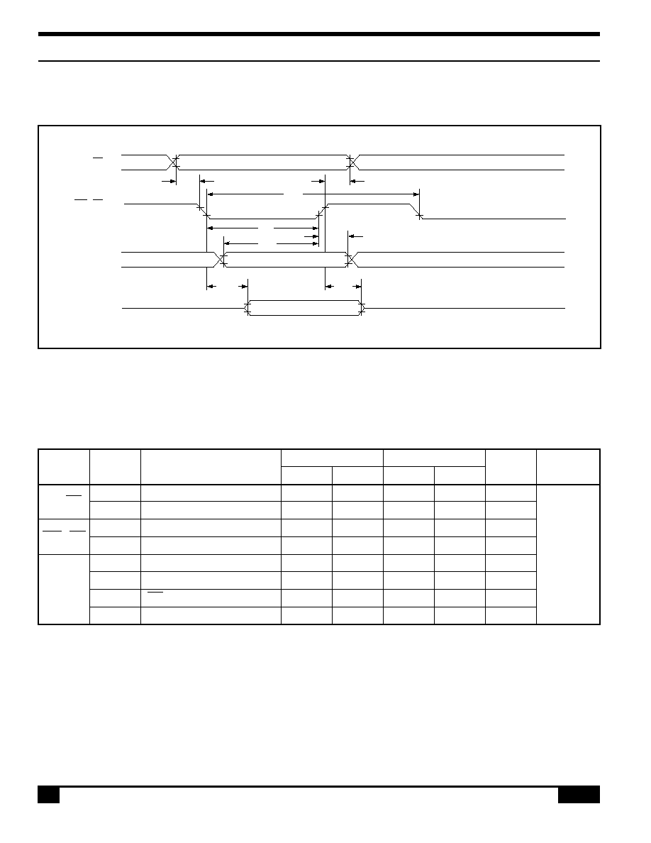
S-MOS Systems, Inc. · 2460 North First Street · San Jose, CA 95131 · Tel: (408) 922-0200 · Fax: (408) 922-0238
62
268-0.4
4.0 Specifications
4.5 4.5.1.1
4.5 SED1335/SED1336 AC Timing Diagrams
4.5.1 8080 family Interface Timing
t
CYC
t
OH8
t
AH8
t
AW8
t
CC
t
DS8
t
DH8
t
ACC8
AO, CS
WR, RD
D0 to D7
(Write)
D0 to D7
(Read)
Figure 39. 8080 family interface timing
4.5.1.1 SED1335F
Signal
Symbol
Parameter
V
DD
= 4.5 to 5.5V V
DD
= 2.7 to 4.5V
Unit
Condition
min
max
min
max
A0, CS
t
AH8
Address hold time
10
--
10
--
ns
t
AW8
Address setup time
0
--
0
--
ns
WR, RD
t
CYC
System cycle time
See note
--
See note
--
ns
t
CC
Strobe pulsewidth
120
--
150
--
ns
CL = 100
t
DS8
Data setup time
120
--
120
--
ns
pF
D0 to D7
t
DH8
Data hold time
5
--
5
--
ns
t
ACC8
RD access time
--
50
--
80
ns
t
OH8
Output disable time
10
50
10
55
ns
Note: For memory control and system control commands:
t
CYC8
= 2t
C
+ t
CC
+ t
CEA
+ 75 > t
ACV
+ 245
For all other commands:
t
CYC8
= 4t
C
+ t
CC
+ 30
T
a
= 20 to 75
°
C
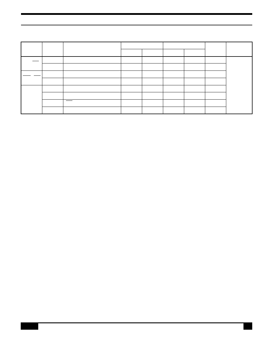
S-MOS Systems, Inc. · 2460 North First Street · San Jose, CA 95131 · Tel: (408) 922-0200 · Fax: (408) 922-0238
268-0.4
63
4.5.1.2
4.0 Specifications
4.5.1.2 SED1336F
Signal
Symbol
Parameter
V
DD
= 4.5 to 5.5V V
DD
= 3.0 to 4.5V
Unit
Condition
min
max
min
max
A0, CS
t
AH8
Address hold time
10
--
10
--
ns
t
AW8
Address setup time
0
--
0
--
ns
WR, RD
t
CYC
System cycle time
See note
--
See note
--
ns
t
CC
Strobe pulsewidth
120
--
140
--
ns
CL = 100
t
DS8
Data setup time
120
--
120
--
ns
pF
D0 to D7
t
DH8
Data hold time
5
--
5
--
ns
t
ACC8
RD access time
--
50
--
70
ns
t
OH8
Output disable time
10
50
10
50
ns
Note: For memory control and system control commands:
t
CYC8
= 2t
C
+ t
CC
+ t
CEA
+ 75 > t
ACV
+ 245
For all other commands:
t
CYC8
= 4t
C
+ t
CC
+ 30
T
a
= 20 to 75
°
C
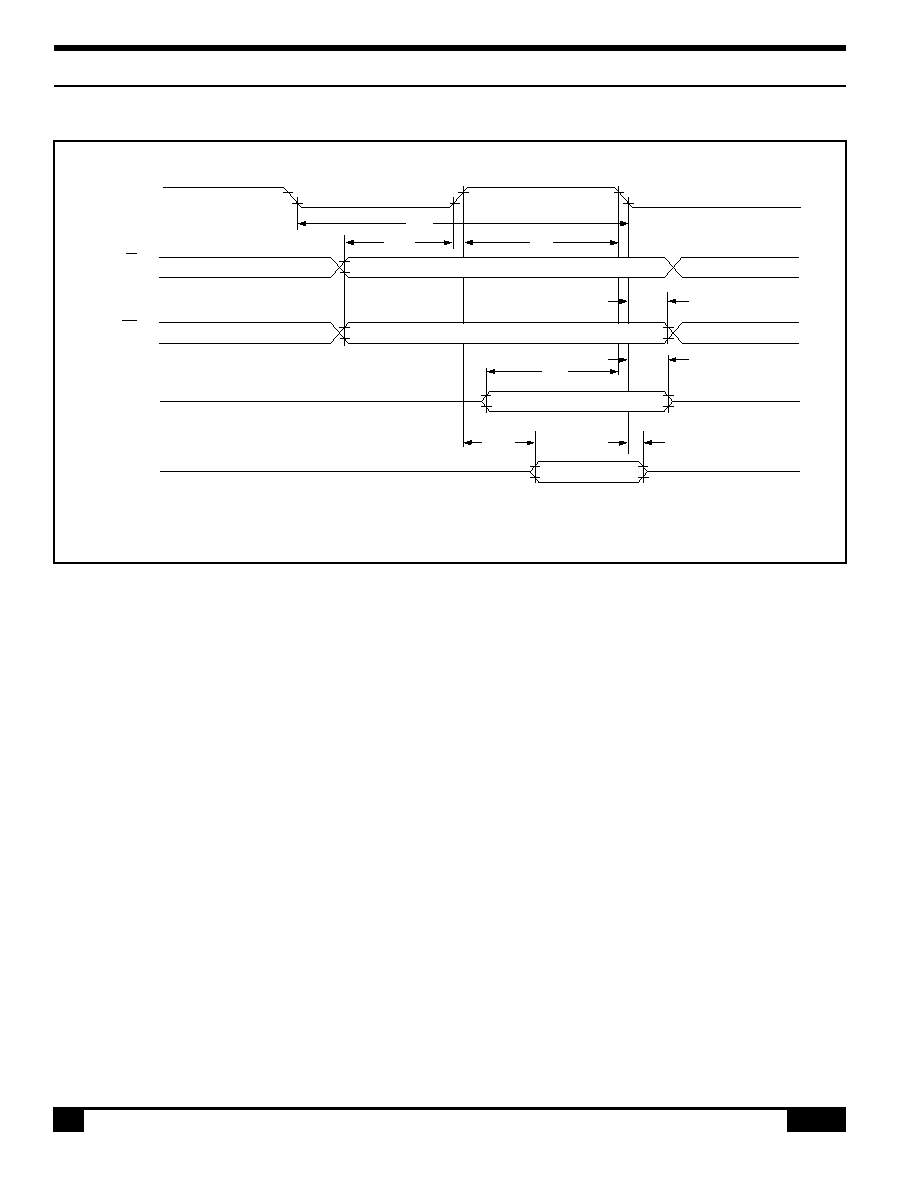
S-MOS Systems, Inc. · 2460 North First Street · San Jose, CA 95131 · Tel: (408) 922-0200 · Fax: (408) 922-0238
64
268-0.4
4.5.2 6800 family Interface Timing
Note: t
CYC6
indicates the interval during which CS is LOW and E is HIGH.
Figure 40. 6800 family interface timing
E
R/W
AO, CS
D0 to D7
(Write)
D0 to D7
(Read)
t
CYC
t
AW6
t
EW
t
AH6
t
DH6
t
DS6
t
OH6
t
ACC6
4.0 Specifications
4.5.2
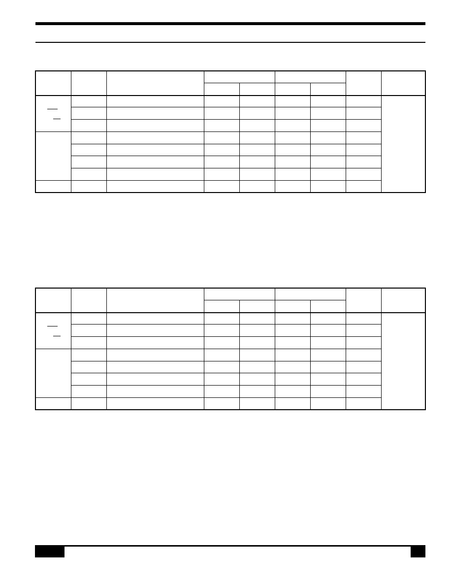
S-MOS Systems, Inc. · 2460 North First Street · San Jose, CA 95131 · Tel: (408) 922-0200 · Fax: (408) 922-0238
268-0.4
65
A0,
CS,
R/W
4.5.2.1 4.5.2.2
4.0 Specifications
4.5.2.1 SED1335F
Signal
Symbol
Parameter
V
DD
= 4.5 to 5.5V V
DD
= 2.7 to 4.5V
Unit
Condition
min
max
min
max
t
CYC6
System cycle time
See note
--
See note
--
ns
t
AW6
Address setup time
0
--
10
--
ns
t
AH6
Address hold time
0
--
0
--
ns
t
DS6
Data setup time
100
--
120
--
ns
CL =
D0 to D7
t
DH6
Data hold time
0
--
0
--
ns
100 pF
t
OH6
Output disable time
10
50
10
75
ns
t
ACC6
Access time
--
85
--
130
ns
E
t
EW
Enable pulsewidth
120
--
150
--
ns
Note: For memory control and system control commands:
t
CYC6
= 2t
C
+ t
EW
+ t
CEA
+ 75 > t
ACV
+ 245
For all other commands:
t
CYC6
= 4t
C
+ t
EW
+ 30
T
a
= 20 to 75
°
C
A0,
CS,
R/W
4.5.2.2 SED1336F
Signal
Symbol
Parameter
V
DD
= 4.5 to 5.5V V
DD
= 3.0 to 4.5V
Unit
Condition
min
max
min
max
t
CYC6
System cycle time
See note
--
See note
--
ns
t
AW6
Address setup time
0
--
10
--
ns
t
AH6
Address hold time
0
--
0
--
ns
t
DS6
Data setup time
100
--
120
--
ns
CL =
D0 to D7
t
DH6
Data hold time
0
--
0
--
ns
100 pF
t
OH6
Output disable time
10
50
10
70
ns
t
ACC6
Access time
--
85
--
120
ns
E
t
EW
Enable pulsewidth
120
--
140
--
ns
Note: For memory control and system control commands:
t
CYC6
= 2t
C
+ t
EW
+ t
CEA
+ 75 > t
ACV
+ 245
For all other commands:
t
CYC6
= 4t
C
+ t
EW
+ 30
T
a
= 20 to 75
°
C
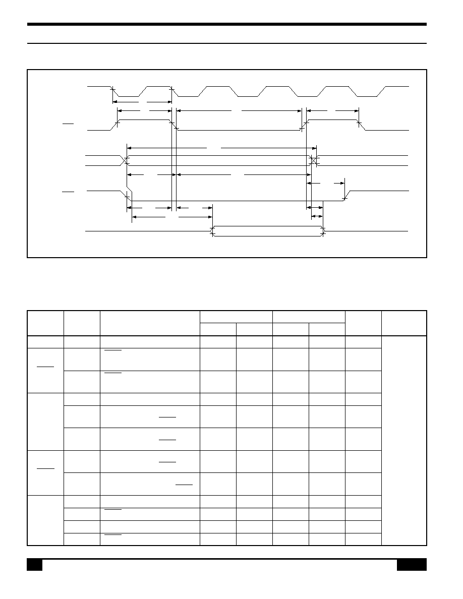
S-MOS Systems, Inc. · 2460 North First Street · San Jose, CA 95131 · Tel: (408) 922-0200 · Fax: (408) 922-0238
66
268-0.4
4.5.3.1 SED1335F
Signal
Symbol
Parameter
V
DD
= 4.5 to 5.5V V
DD
= 2.7 to 4.5V
Unit
Condition
min
max
min
max
EXT
0
t
C
Clock period
100
--
125
--
ns
t
W
VCE HIGH-level pulse-
t
C
50
--
t
C
50
--
ns
VCE
width
t
CE
VCE LOW-level pulse-
2t
C
30
--
2t
C
30
--
ns
width
t
CYR
Read cycle time
3t
C
--
3t
C
--
ns
t
ASC
Address setup time to
t
C
70
--
t
C
100
--
ns
falling edge of VCE
t
AHC
Address hold time from
2t
C
30
--
2t
C
40
--
ns
falling edge of VCE
t
RCS
Read cycle setup time to
t
C
45
--
t
C
60
--
ns
VRD
falling edge of VCE
t
RCH
Read cycle hold time
0.5t
C
--
0.5t
C
--
ns
from rising edge of VCE
t
ACV
Address access time
--
3t
C
100
--
3t
C
115
ns
VD0 to
t
CEA
VCE access time
--
2t
C
80
--
2t
C
90
ns
VD7
t
OH2
Output data hold time
0
--
0
--
ns
t
CE3
VCE to data off time
0
--
0
--
ns
4.0 Specifications
4.5.3 4.5.3.1
4.5.3 Display Memory Read Timing
EXT
0
VCE
VA0 to VA15
VRD
VD0 to VD7
(SED1335F)
t
C
t
W
t
CE
t
W
t
AHC
t
ASC
t
CYR
t
RCS
t
CEA
t
RCH
t
CE3
t
OH2
t
ACV
Figure 41. Display memory read timing
VA0 to
VA15
CL = 100
pF
T
a
= 20 to 75
°
C
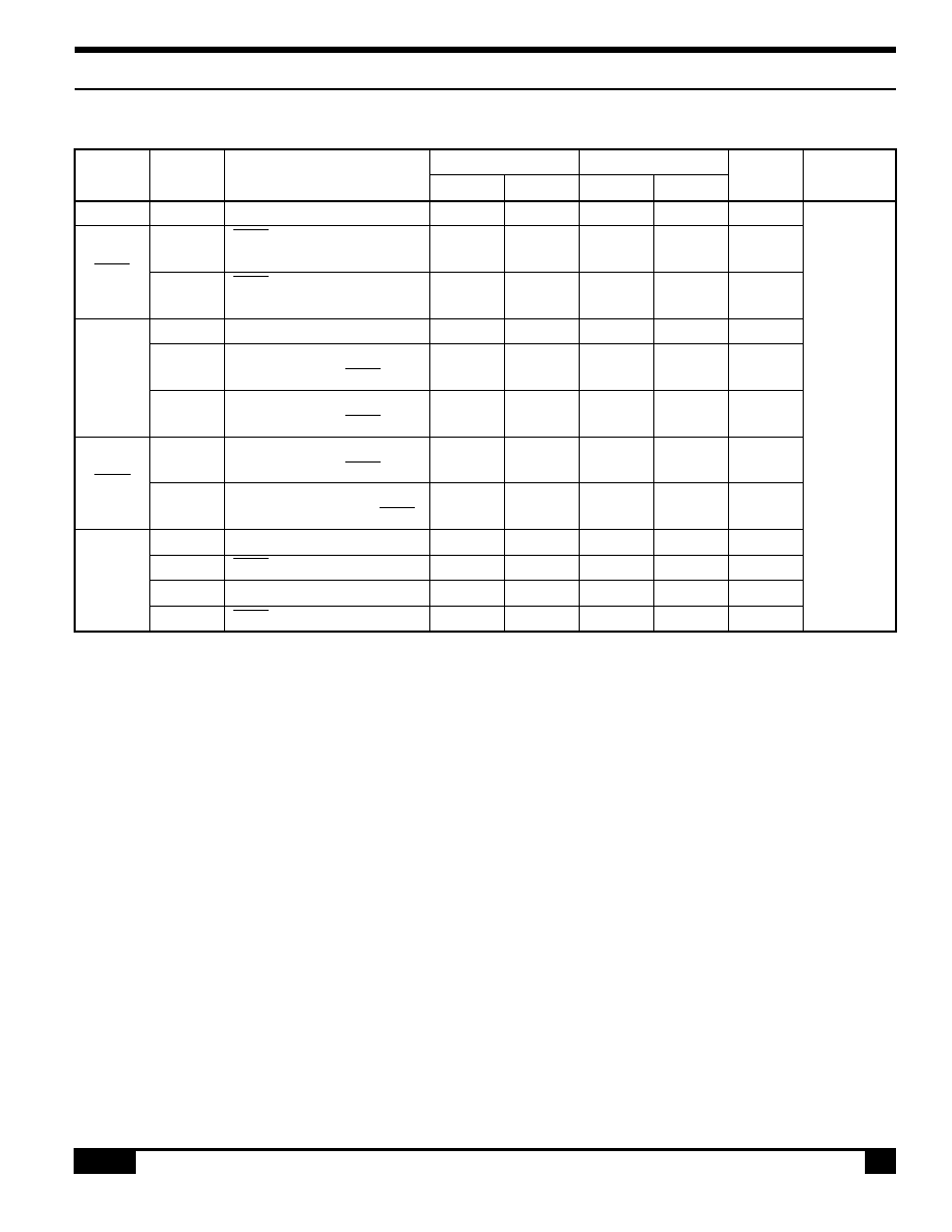
S-MOS Systems, Inc. · 2460 North First Street · San Jose, CA 95131 · Tel: (408) 922-0200 · Fax: (408) 922-0238
268-0.4
67
4.5.3.2
4.0 Specifications
4.5.3.2 SED1336F
Signal
Symbol
Parameter
V
DD
= 4.5 to 5.5V V
DD
= 3.0 to 4.5V
Unit
Condition
min
max
min
max
EXT
0
t
C
Clock period
100
--
125
--
ns
t
W
VCE HIGH-level pulse-
t
C
50
--
t
C
50
--
ns
VCE
width
t
CE
VCE LOW-level pulse-
2t
C
30
--
2t
C
30
--
ns
width
t
CYR
Read cycle time
3t
C
--
3t
C
--
ns
t
ASC
Address setup time to
t
C
70
--
t
C
100
--
ns
falling edge of VCE
t
AHC
Address hold time from
2t
C
30
--
2t
C
40
--
ns
falling edge of VCE
t
RCS
Read cycle setup time to
t
C
45
--
t
C
55
--
ns
VRD
falling edge of VCE
t
RCH
Read cycle hold time
0.5t
C
--
0.5t
C
--
ns
from rising egde of VCE
t
ACV
Address access time
--
3t
C
100
--
3t
C
110
ns
VD0 to
t
CEA
VCE access time
--
2t
C
80
--
2t
C
85
ns
VD7
t
OH2
Output data hold time
0
--
0
--
ns
t
CE3
VCE to data off time
0
--
0
--
ns
VA0 to
VA15
CL = 100
pF
T
a
= 20 to 75
°
C
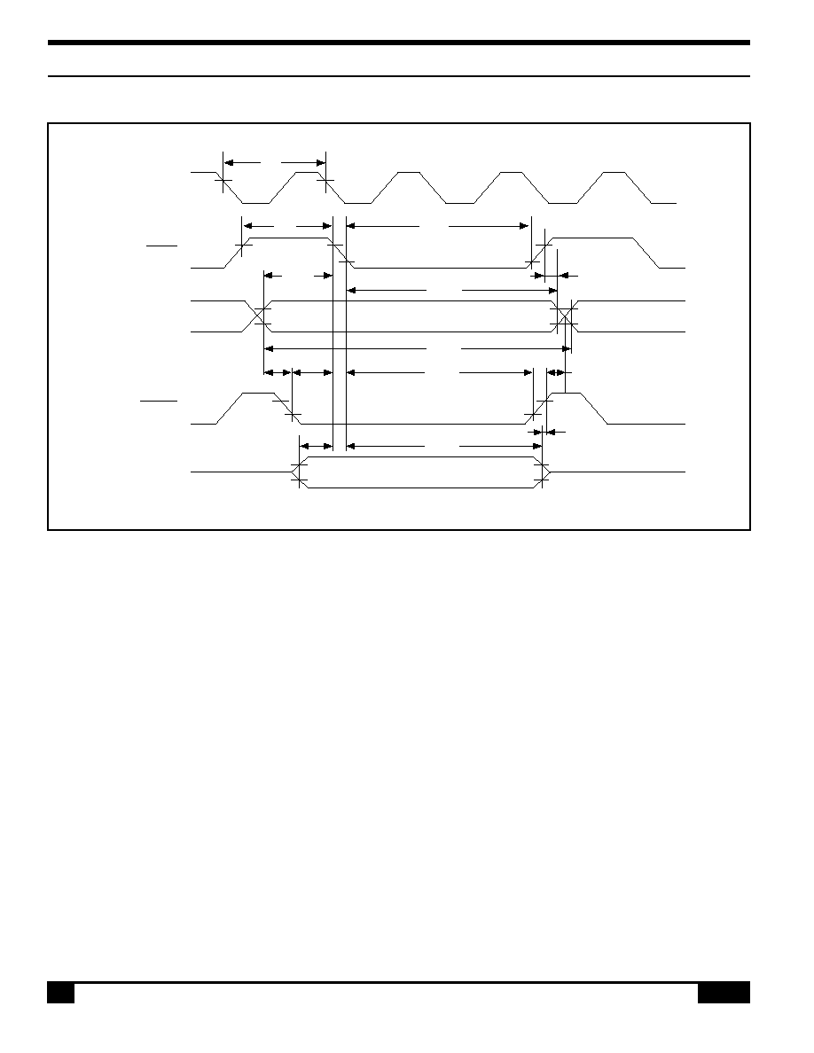
S-MOS Systems, Inc. · 2460 North First Street · San Jose, CA 95131 · Tel: (408) 922-0200 · Fax: (408) 922-0238
68
268-0.4
4.0 Specifications
4.5.4
4.5.4 Display Memory Write Timing
t
WSC
t
C
t
CE
t
CYW
t
AH2
t
CA
t
OH2
t
ASC
t
WHC
t
AS
t
OHC
t
OSC
t
AHC
t
W
EXT
O
VCE
VA0~VA15
VWR
VD0~VD7
Figure 42. Display memory write timing
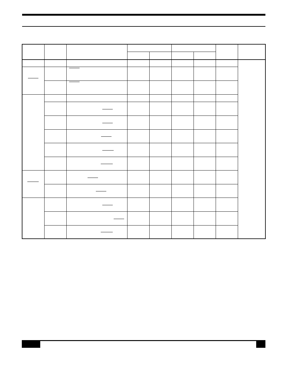
S-MOS Systems, Inc. · 2460 North First Street · San Jose, CA 95131 · Tel: (408) 922-0200 · Fax: (408) 922-0238
268-0.4
69
4.5.4.1 SED1335F
Signal
Symbol
Parameter
V
DD
= 4.5 to 5.5V V
DD
= 2.7 to 4.5V
Unit
Condition
min
max
min
max
EXT
0
t
C
Clock period
100
--
125
--
ns
t
W
VCE HIGH-level pulse-
t
C
50
--
t
C
50
--
ns
VCE
width
t
CE
VCE LOW-level pulse-
2t
C
30
--
2t
C
30
--
ns
width
t
CYW
Write cycle time
3t
C
--
3t
C
--
ns
t
AHC
Address hold time from
2t
C
30
--
2t
C
40
--
ns
falling edge of VCE
t
ASC
Address setup time to
t
C
70
--
t
C
110
--
ns
falling edge of VCE
VA0 to
t
CA
Address hold time from
0
--
0
--
ns
VA15
rising edge of VCE
t
AS
Address setup time to
0
--
0
--
ns
falling edge of VWR
t
AH2
Address hold time from
10
--
10
--
ns
rising edge of VWR
t
WSC
Write setup time to falling
t
C
80
--
t
C
115
--
ns
VWR
edge of VCE
t
WHC
Write hold time from fall-
2t
C
20
--
2t
C
20
--
ns
ing edge of VCE
t
DSC
Data input setup time to
t
C
85
--
t
C
125
--
ns
falling edge of VCE
VD0 to
t
DHC
Data input hold time
2t
C
30
--
2t
C
30
--
ns
VD7
from falling edge of VCE
t
DH2
Data hold time from
5
50
5
50
ns
rising edge of VWR
Note: VD0 to VD7 are latching input/outputs. While the bus is high impedance, VD0 to VD7 retain the write data until the data read
from the memory is placed on the bus.
4.5.4.1
4.0 Specifications
T
a
= 20 to 75
°
C
CL = 100
pF
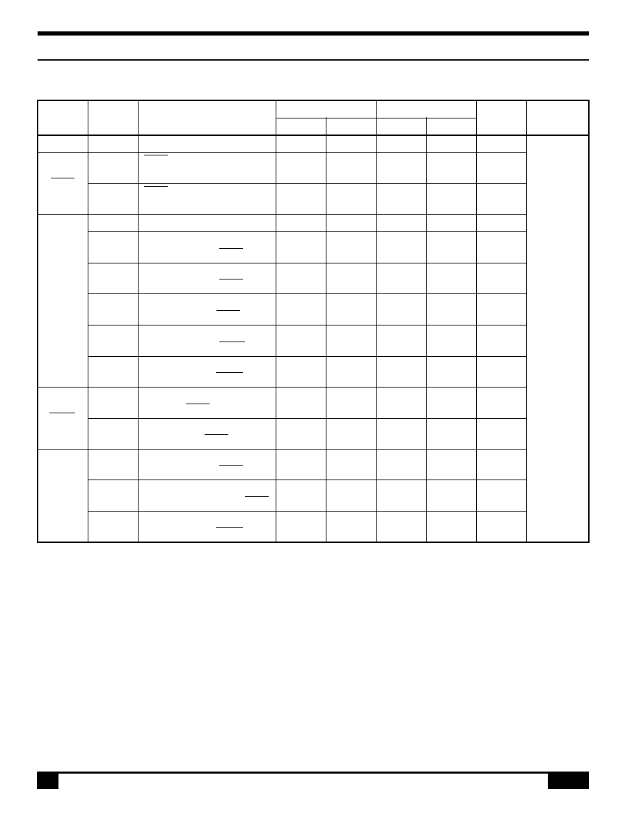
S-MOS Systems, Inc. · 2460 North First Street · San Jose, CA 95131 · Tel: (408) 922-0200 · Fax: (408) 922-0238
70
268-0.4
4.5.4.2 SED1336F
Signal
Symbol
Parameter
V
DD
= 4.5 to 5.5V V
DD
= 3.0 to 4.5V
Unit
Condition
min
max
min
max
EXT
0
t
C
Clock period
100
--
125
--
ns
t
W
VCE HIGH-level pulse-
t
C
50
--
t
C
50
--
ns
VCE
width
t
CE
VCE LOW-level pulse-
2t
C
30
--
2t
C
30
--
ns
width
t
CYW
Write cycle time
3t
C
--
3t
C
--
ns
t
AHC
Address hold time from
2t
C
30
--
2t
C
40
--
ns
falling edge of VCE
t
ASC
Address setup time to
t
C
70
--
t
C
100
--
ns
falling edge of VCE
VA0 to
t
CA
Address hold time from
0
--
0
--
ns
VA15
rising edge of VCE
t
AS
Address setup time to
0
--
0
--
ns
falling edge of VWR
t
AH2
Address hold time from
10
--
10
--
ns
rising edge of VWR
t
WSC
Write setup time to falling
t
C
80
--
t
C
110
--
ns
VWR
edge of VCE
t
WHC
Write hold time from fall-
2t
C
20
--
2t
C
20
--
ns
ing edge of VCE
t
DSC
Data input setup time to
t
C
85
--
t
C
120
--
ns
falling edge of VCE
VD0 to
t
DHC
Data input hold time
2t
C
30
--
2t
C
30
--
ns
VD7
from falling edge of VCE
t
DH2
Data hold time from
5
50
5
50
ns
rising edge of VWR
Note: VD0 to VD7 are latching input/outputs. While the bus is high impedance, VD0 to VD7 retain the write data until the data read
from the memory is placed on the bus.
T
a
= 20 to 75
°
C
CL = 100
pF
4.0 Specifications
4.5.4.2
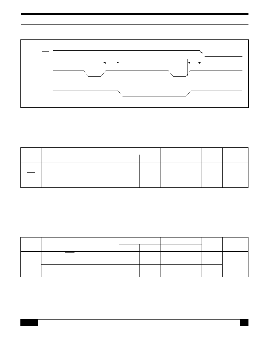
S-MOS Systems, Inc. · 2460 North First Street · San Jose, CA 95131 · Tel: (408) 922-0200 · Fax: (408) 922-0238
268-0.4
71
4.5.5 4.5.5.2
4.0 Specifications
4.5.5 SLEEP IN Command Timing
VCE
WR
(command input)
YDIS
t
WRL
t
WRD
SYSTEM SET write
SLEEP IN write
Figure 43. SLEEP IN command timing
4.5.5.1 SED1335F
Signal
Symbol
Parameter
V
DD
= 4.5 to 5.5V V
DD
= 2.7 to 4.5V
Unit
Condition
min
max
min
max
t
WRD
VCE falling-edge delay
See note 1
--
See note 1
--
ns
WR
time
t
WRL
YDIS falling-edge delay
--
See note 2
--
See note 2
ns
time
Notes:
1. t
WRD
= 18t
C
+ t
OSS
+ 40 (t
OSS
is the time delay from the sleep state until stable operation)
2. t
WRL
= 36t
C
×
[TC/R]
×
[L/F] + 70
T
a
= 20 to 75
°
C
CL = 100
pF
4.5.5.2 SED1336F
Signal
Symbol
Parameter
V
DD
= 4.5 to 5.5V V
DD
= 3.0 to 4.5V
Unit
Condition
min
max
min
max
t
WRD
VCE falling-edge delay
See note 1
--
See note 1
--
ns
WR
time
t
WRL
YDIS falling-edge delay
--
See note 2
--
See note 2
ns
time
Notes:
1. t
WRD
= 18t
C
+ t
OSS
+ 40 (t
OSS
is the time delay from the sleep state until stable operation)
2. t
WRL
= 36t
C
×
[TC/R]
×
[L/F] + 70
T
a
= 20 to 75
°
C
CL = 100
pF
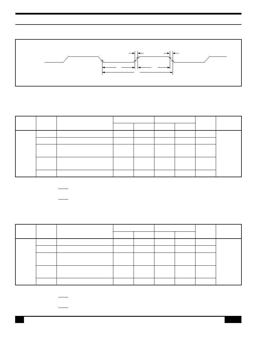
S-MOS Systems, Inc. · 2460 North First Street · San Jose, CA 95131 · Tel: (408) 922-0200 · Fax: (408) 922-0238
72
268-0.4
4.0 Specifications
4.5.6 4.5.6.2
4.5.6 External Oscillator Signal Timing
EXT
0
t
WL
t
WH
t
CL
t
RCL
t
FCL
Figure 44. External oscillator signal timing
4.5.6.1 SED1335F
Signal
Symbol
Parameter
V
DD
= 4.5 to 5.5V V
DD
= 2.7 to 4.5V
Unit
Condition
min
max
min
max
t
RCL
External clock rise time
--
15
--
15
ns
t
FCL
External clock fall time
--
15
--
15
ns
t
WH
External clock
See note 1 See note 2 See note 1 See note 2
ns
HIGH-level pulsewidth
t
WL
External clock
See note 1 See note 2 See note 1 See note 2
ns
LOW-level pulsewidth
t
C
External clock period
100
--
125
--
ns
Notes:
1.
(t
C
t
RCL
t
FCL
)
×
475
< t
WH
, t
WL
1000
2.
(t
C
t
RCL
t
FCL
)
×
525
> t
WH
, t
WL
1000
T
a
= 20 to 75
°
C
EXT
0
4.5.6.2 SED1336F
Signal
Symbol
Parameter
V
DD
= 4.5 to 5.5V V
DD
= 3.0 to 4.5V
Unit
Condition
min
max
min
max
t
RCL
External clock rise time
--
15
--
15
ns
t
FCL
External clock fall time
--
15
--
15
ns
t
WH
External clock
See note 1 See note 2 See note 1 See note 2
ns
HIGH-level pulsewidth
t
WL
External clock
See note 1 See note 2 See note 1 See note 2
ns
LOW-level pulsewidth
t
C
External clock period
100
--
125
--
ns
Notes:
1.
(t
C
t
RCL
t
FCL
)
×
475
< t
WH
, t
WL
1000
2.
(t
C
t
RCL
t
FCL
)
×
525
> t
WH
, t
WL
1000
T
a
= 20 to 75
°
C
EXT
0
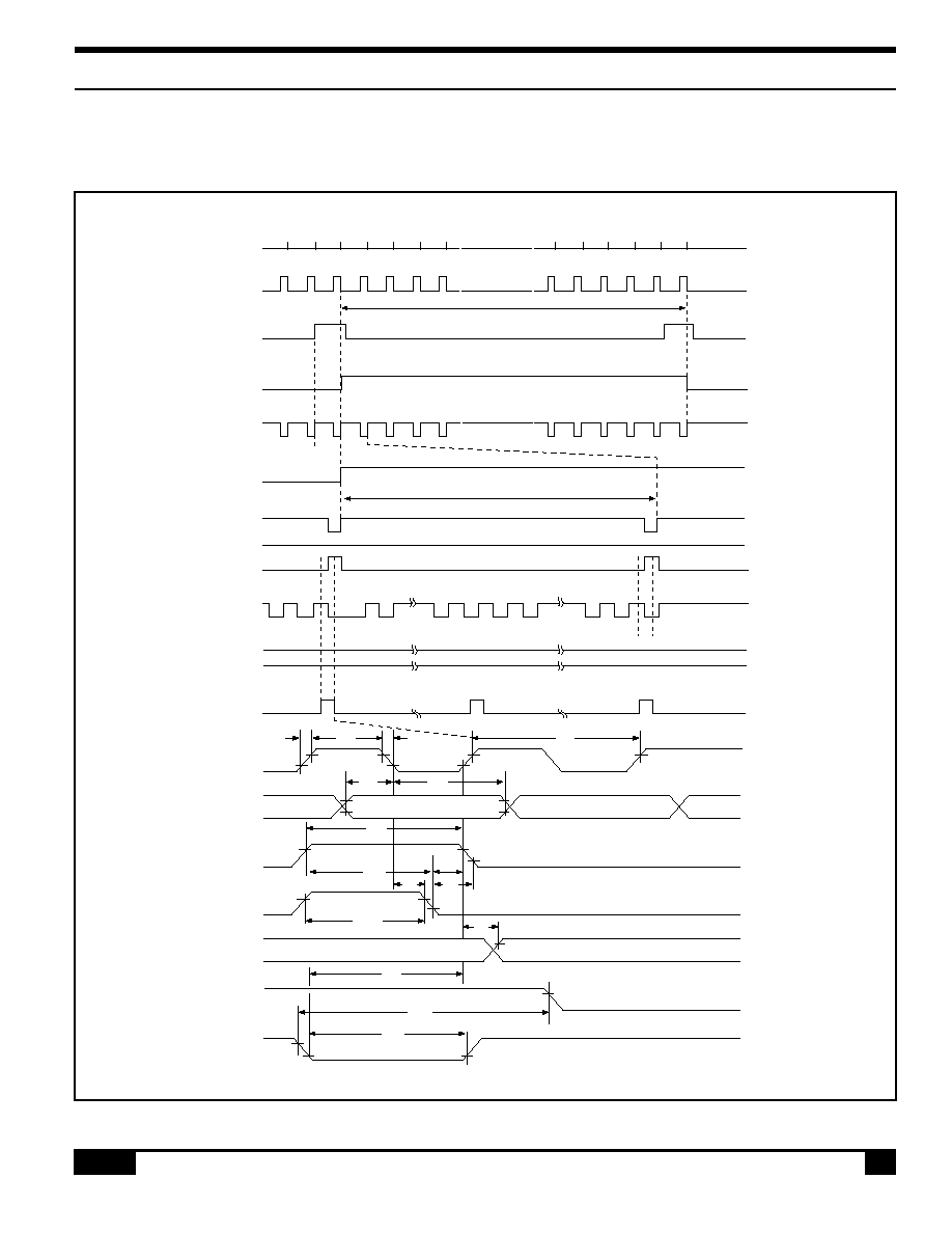
S-MOS Systems, Inc. · 2460 North First Street · San Jose, CA 95131 · Tel: (408) 922-0200 · Fax: (408) 922-0238
268-0.4
73
4.5.7
4.0 Specifications
4.5.7 LCD Output Timing
The following characteristics are for a 1/64 duty cycle.
Figure 45. LCD output timing
t
WX
t
DS
t
LD
t
WY
t
DHY
t
L1
t
L2
t
WL
t
DH
t
CX
t
r
t
f
1 frame period
1 line period
ROW1
ROW2
ROW64
t
S2
t
S1
ROW
LP
YD
WF
YSCL
62
63
64
1
2
3
4
WF
YSCL
LP
XSCL
XD0~XD3
XECL
XSCL
XD0~XD3
LP
XECL
WF(B)
YD
YSCL
t
WXE
t
Df
60
61
62
63
64
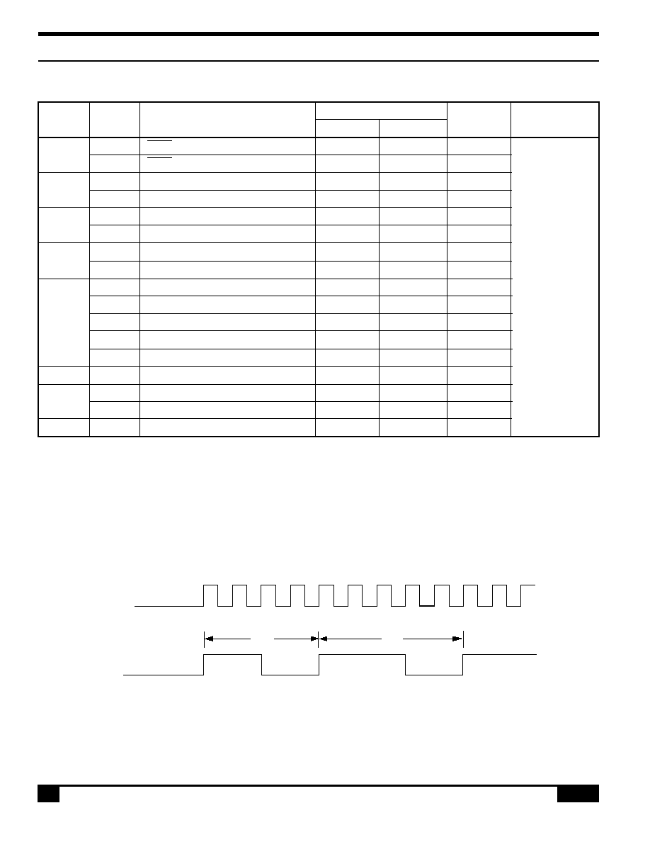
S-MOS Systems, Inc. · 2460 North First Street · San Jose, CA 95131 · Tel: (408) 922-0200 · Fax: (408) 922-0238
74
268-0.4
4.0 Specifications
4.5.7
Signal
Symbol
Parameter
Rating
Unit
Condition
min
max
t
r
VCE high level pulse width
--
35
ns
t
f
VCE low level pulse width
--
35
ns
XSCL
t
CX
Shift clock cycle time
4tc
70
--
ns
t
WX
XSCL clock pulse width
2t
C80
--
ns
XD0
t
DH
X-data hold time
2t
C100
--
ns
V
DD
= 5.0V
to XD3
t
DS
X-data setup time
2t
C100
--
ns
±
10%
LP
t
LS
Latch data setup time
2t
C100
--
ns
CL=150F
t
WL
LP signal pulse width
4t
C80
--
ns
t
L1
XECL setup time
3t
C100
--
ns
t
L2
XECL data hold time
t
C30
--
ns
XECL
t
S1
Enable setup time
t
C30
--
ns
t
S1
Enable delay time
t
C30
--
ns
t
WXE
XECL clock pulse width
3t
C80
--
ns
WF
t
DF
Time allowance of WF delay
--
100
ns
YSCL
t
LD
LP delay time against YSCL
4t
C100
--
ns
t
WY
YSCL clock pulse width
4t
C80
--
ns
YD
t
DHY
Y-data hold time
6t
C100
--
ns
t
C
ø0
XSCL
5 t
C
4
Notes:
1. The E-1330 reads display memory data from the address of the top left corner of the display screen, then scans horizontally until
it reaches the address for the bottom right corner of the display screen. Therefore, each line of X-driver data is sent starting from
the left side of the display line.
2. The E-1330 uses nine cycles of ø0 as the basic cycle (t
c
). The XSCL waveform is shown in the following figure.
T
a
= 20 to 75
°
C
4.5.7.1 SED1330F
S-MOS Systems, Inc. · 2460 North First Street · San Jose, CA 95131 · Tel: (408) 922-0200 · Fax: (408) 922-0238
268-0.4
75
4.5.7.2 4.5.7.3
4.0 Specifications
4.5.7.2 SED1335F
Signal
Symbol
Parameter
V
DD
= 4.5 to 5.5V V
DD
= 2.7 to 4.5V
Unit
Condition
min
max
min
max
t
r
Rise time
--
30
--
40
ns
t
f
Fall time
--
30
--
40
ns
XSCL
t
CX
Shift clock cycle time
4t
C
--
4t
C
--
ns
t
WX
XSCL clock pulsewidth
2t
C
60
--
2t
C
60
--
ns
XD0 to
t
DH
X data hold time
2t
C
50
--
2t
C
50
--
ns
XD3
t
DS
X data setup time
2t
C
100
--
2t
C
105
--
ns
t
LS
Latch data setup time
2t
C
50
--
2t
C
50
--
ns
LP
t
WL
LP pulsewidth
4t
C
80
--
4t
C
120
--
ns
t
LD
LP delay time from XSCL
0
--
0
--
ns
WF
t
DF
Permitted WF delay
--
50
--
50
ns
YD
t
DHY
Y data hold time
2t
C
20
--
2t
C
20
--
ns
T
a
= 20 to 75
°
C
4.5.7.3 SED1336F
Signal
Symbol
Parameter
V
DD
= 4.5 to 5.5V V
DD
= 3.0 to 4.5V
Unit
Condition
min
max
min
max
t
r
Rise time
--
30
--
35
ns
t
f
Fall time
--
30
--
35
ns
XSCL
t
CX
Shift clock cycle time
4t
C
--
4t
C
--
ns
t
WX
XSCL clock pulsewidth
2t
C
60
--
2t
C
60
--
ns
XD0 to
t
DH
X data hold time
2t
C
50
--
2t
C
50
--
ns
XD3
t
DS
X data setup time
2t
C
100
--
2t
C
100
--
ns
t
LS
Latch data setup time
2t
C
50
--
2t
C
50
--
ns
LP
t
WL
LP pulsewidth
4t
C
80
--
4t
C
100
--
ns
t
LD
LP delay time from XSCL
0
--
0
--
ns
WF
t
DF
Permitted WF delay
--
50
--
50
ns
YD
t
DHY
Y data hold time
2t
C
20
--
2t
C
20
--
ns
Note: The SED1335F/1336F reads display memory data from the address of the top left corner of the display screen, then scans
horizontally until it reaches the address for the bottom right corner of the display screen. Therefore, each line of X-driver data
is sent starting from the left side of the display line.
T
a
= 20 to 75
°
C
CL =
100 pF
CL =
100 pF

S-MOS Systems, Inc. · 2460 North First Street · San Jose, CA 95131 · Tel: (408) 922-0200 · Fax: (408) 922-0238
76
268-0.4
THIS PAGE INTENTIONALLY BLANK

S-MOS Systems, Inc. · 2460 North First Street · San Jose, CA 95131 · Tel: (408) 922-0200 · Fax: (408) 922-0238
268-0.4
77
5.0
Display Control Functions

S-MOS Systems, Inc. · 2460 North First Street · San Jose, CA 95131 · Tel: (408) 922-0200 · Fax: (408) 922-0238
78
268-0.4
THIS PAGE INTENTIONALLY BLANK
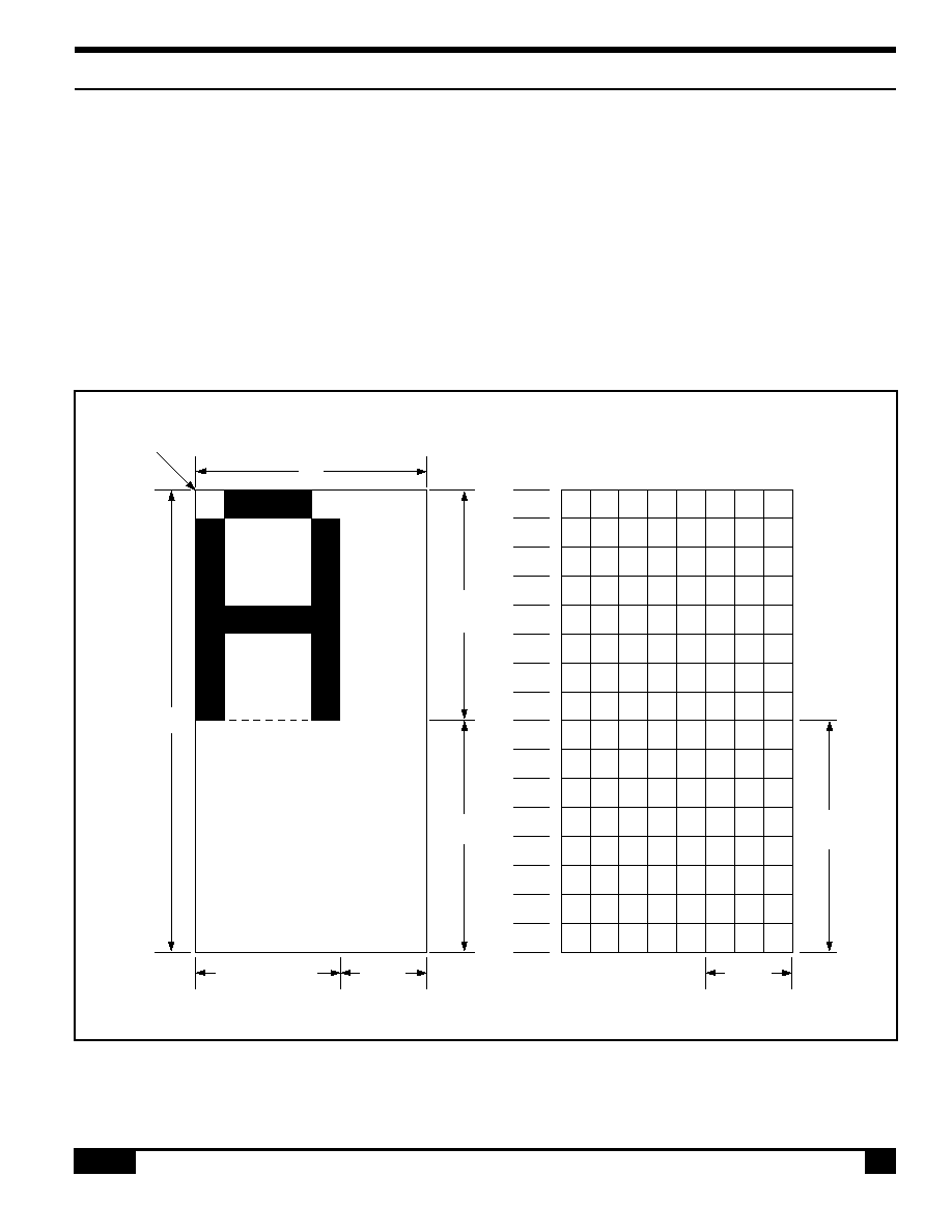
S-MOS Systems, Inc. · 2460 North First Street · San Jose, CA 95131 · Tel: (408) 922-0200 · Fax: (408) 922-0238
268-0.4
79
5.0 5.1
5.0 Display Control Functions
5.0 Display Control Functions
5.1 Character Configuration
The origin of each character bitmap is in the top left
corner as shown in Figure 38. Adjacent bits in each
byte are horizontally adjacent in the corresponding
character image.
Although the size of the bitmap is fixed by the charac-
ter generator, the actual displayed size of the charac-
ter field can be varied in both dimensions.
If the area outside the character bitmap contains only
zeros, the displayed character size can easily be
increased by increasing FX and FY, as the zeros
ensure that the extra space between displayed char-
acters is blank.
The displayed character width can be set to any value
up to 16 even if each horizontal row of the bitmap is
two bytes wide.
0
1
1
1
1
1
1
0
0
0
0
0
0
0
0
0
1
0
0
0
1
0
0
0
0
0
0
0
0
0
0
0
1
0
0
0
1
0
0
0
0
0
0
0
0
0
0
0
1
0
0
0
1
0
0
0
0
0
0
0
0
0
0
0
0
1
1
1
1
1
1
0
0
0
0
0
0
0
0
0
0
0
0
0
0
0
0
0
0
0
0
0
0
0
0
0
0
0
0
0
0
0
0
0
0
0
0
0
0
0
0
0
0
0
0
0
0
0
0
0
0
0
0
0
0
0
0
0
R0
R1
R2
R3
R4
R5
R6
R7
R8
R9
R10
R11
R12
R13
R14
R15
D7
to
D0
FX
Character
height
Space
Character width
Space
FY
Character starting point
Space
data
Space
data
Figure 46. Example of character display ([FX]
8) and generator bitmap
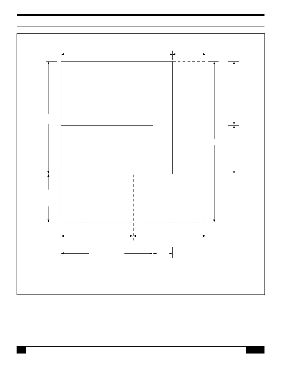
S-MOS Systems, Inc. · 2460 North First Street · San Jose, CA 95131 · Tel: (408) 922-0200 · Fax: (408) 922-0238
80
268-0.4
5.0 Display Control Functions
5.1
FY
Vertical
non-display
area
Character
Height
Space
16 dots
Horizontal
non-display
area
FX
8 dots
8 dots
Space
Character width
Note: The SED1330F/1335F/1336F does not automatically insert spaces between characters. If the displayed character size is
8 pixels or less and the space between character origins is nine pixels or more, the bitmap must use two bytes per row,
even though the character image requires only one.
Figure 47. Character width greater than one byte wide ([FX] = 9)
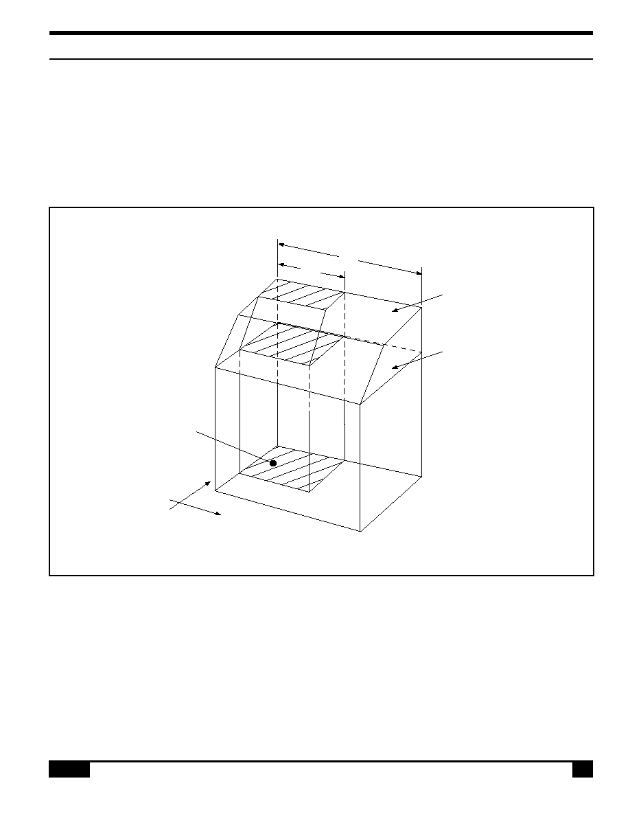
S-MOS Systems, Inc. · 2460 North First Street · San Jose, CA 95131 · Tel: (408) 922-0200 · Fax: (408) 922-0238
268-0.4
81
5.2 5.2.2
5.0 Display Control Functions
5.2 Screen Configuration
5.2.1 Screen Configuration
The basic screen configuration of the SED1330F/
1335F/1336F is as a single text screen or as overlap-
ping text and graphics screens. The graphics screen
uses eight times as much display memory as the text
screen.
A/P
Character
memory area
Graphics
memory area
(XM,YM)
(XM,0)
(0,0)
(0,YM)
(XW,YM)
0800H
0000H
Display
memory
window
07FFH
47FFH
C/R
Y
X
Figure 48. Virtual and physical screen relationship
5.2.2 Display Address Scanning
The SED1330F/1335F/1336F scans the display memory
in the same way as a raster scan CRT screen. Each row
is scanned from left to right until the address range
equals C/R. Rows are scanned from top to bottom.
In graphics mode, at the start of each line, the address
counter is set to the address at the start of the previous
line plus the address pitch, AP.
In text mode, the address counter is set to the same
start address, and the same character data is read, for
each row in the character bitmap. However, a new row
of the character generator output is used each time.
Once all the rows in the character bitmap have been
displayed, the address counter is set to the start
address plus AP and the next line of text is displayed.
Figure 40 shows the relationship between the virtual
screens and the physical screen.
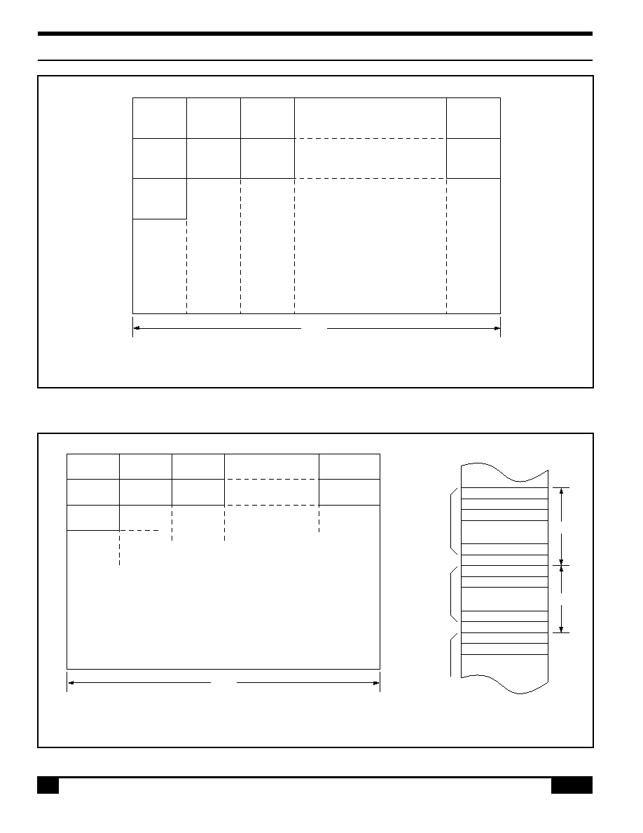
S-MOS Systems, Inc. · 2460 North First Street · San Jose, CA 95131 · Tel: (408) 922-0200 · Fax: (408) 922-0238
82
268-0.4
5.0 Display Control Functions
5.2.2
W/S = 0, FX = 8, FY = 8
C/R
1
·
·
·
8
9
·
·
·
16
17
·
·
·
24
·
·
·
·
SAD
SAD + AP
SAD + 2AP
SAD + 1
SAD + AP
+ 1
SAD + 2
SAD + AP
+ 2
SAD + C/R
SAD + AP
+ C/R
Note: One byte of display memory corresponds to one character.
Figure 49. Character position parameters
SAD
SAD + AP
SAD + 2AP
SAD +1
SAD + AP
+ 1
SAD + 2
SAD + AP
+ 2
SAD + C/R
SAD + AP
+ C/R
1
2
3
·
·
·
·
·
·
·
·
W/S = 0, FX = 8
C/R
SAD
SAD +1
SAD + 2
SAD + C/R
SAD + AP
SAD + AP + 1
SAD + AP + C/R
SAD + 2AP
Line 1
Line 2
Line 3
AP
AP
Note: One bit of display memory corresponds to one pixel.
Figure 50. Character parameters vs. memory
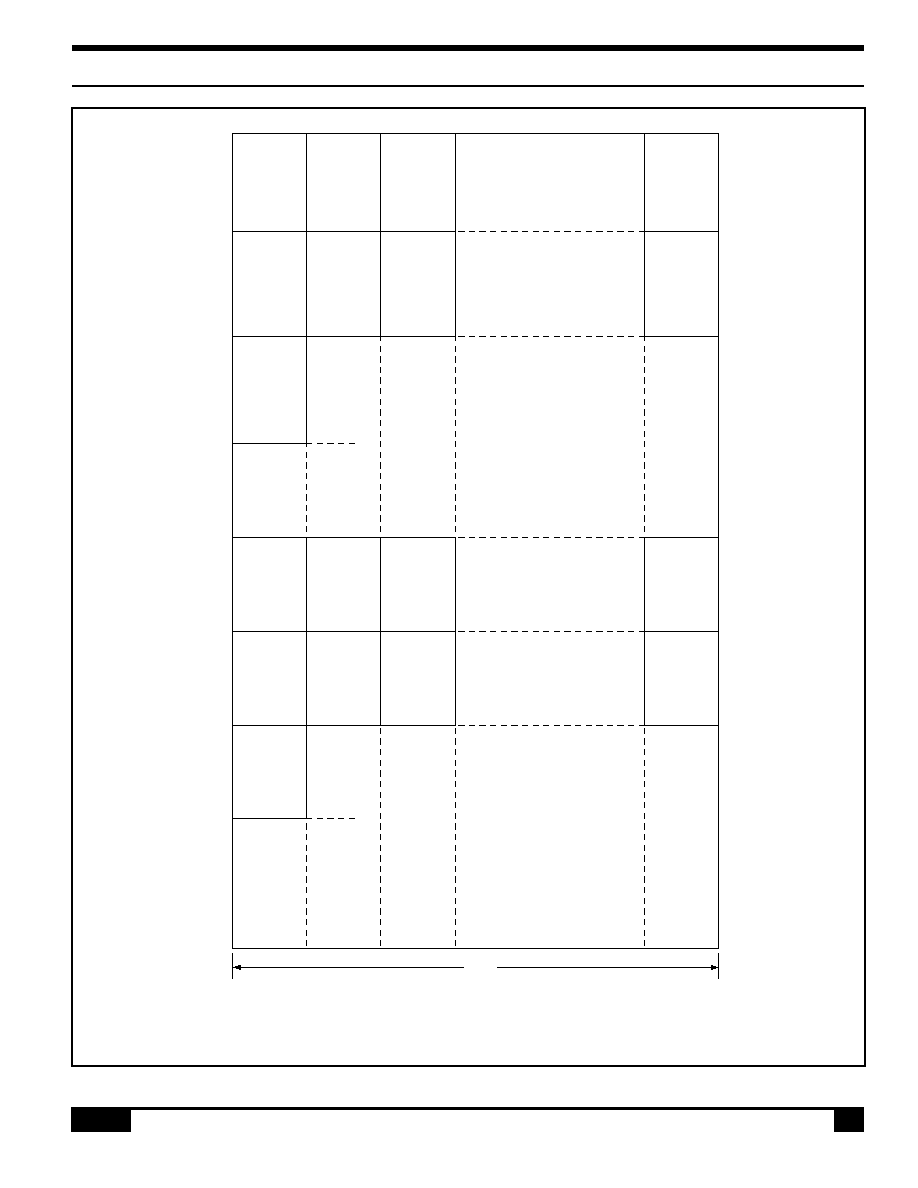
S-MOS Systems, Inc. · 2460 North First Street · San Jose, CA 95131 · Tel: (408) 922-0200 · Fax: (408) 922-0238
268-0.4
83
5.2.2
5.0 Display Control Functions
Figure 51. Two-panel display address indexing
Note: In two-panel drive, the SED1330F/1335F/1336F reads line 1 and line
+ 1 as one cycle. The upper and lower panels are
thus read alternately, one line at a time.
SAD1
SAD1 + 1
SAD1 + 2
SAD1 + C/R
SAD1 + AP
SAD1 + AP
+ 1
SAD1 + AP
+ 2
SAD1 + AP
+ C/R
SAD1 + 2AP
SAD3 + 1
SAD3 + 2
SAD3 + C/R
SAD3 + AP
SAD3 + AP
+ 1
SAD3 + AP
+ 2
SAD3 + AP
+ C/R
SAD3 + 2AP
1
·
·
·
8
9
·
·
·
16
17
·
·
·
24
25
·
·
·
(L/F)/2 =
+ 1
·
·
·
+ 8
+ 9
·
·
·
+ 16
+ 17
·
·
·
+ 24
+ 25
·
·
·
·
(L/F)
W/S = 1, FX = 8, FY = 8
C/R
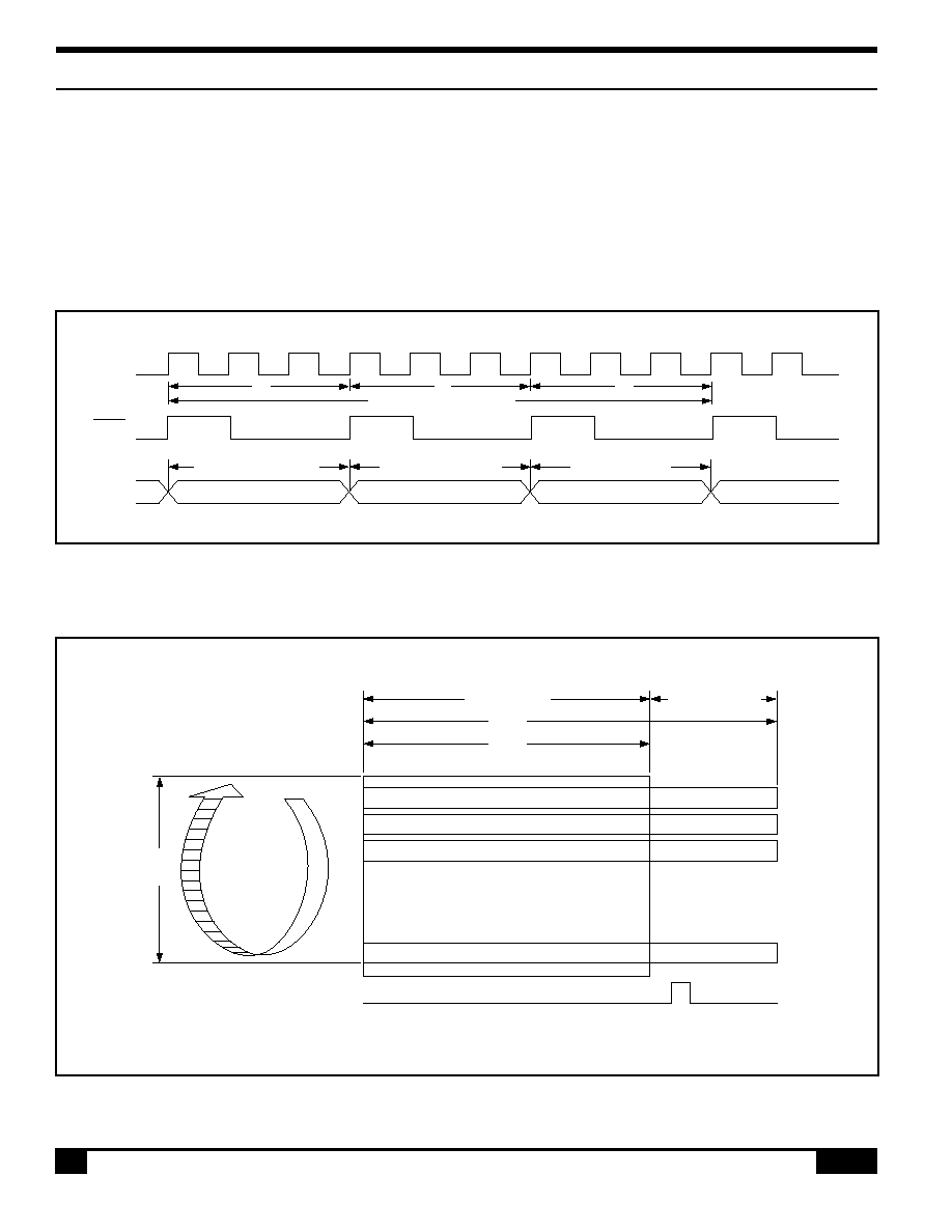
S-MOS Systems, Inc. · 2460 North First Street · San Jose, CA 95131 · Tel: (408) 922-0200 · Fax: (408) 922-0238
84
268-0.4
5.0 Display Control Functions
5.2.3
5.2.3 Display Scan Timing
Figure 44 shows the basic timing of the SED1330F/
1335F/1336F. One display memory read cycle takes
nine periods of the system clock,
0 (f
OSC
). This cycle
repeats (C/R + 1) times per display line.
When reading, the display memory pauses at the end
of each line for (TC/R C/R) display memory read
cycles, though the LCD drive signals are still gener-
ated. TC/R may be set to any value within the con-
straints imposed by C/R, f
OSC
, f
FR
, and the size of the
LCD panel, and it may be used to fine tune the frame
frequency. The microprocessor may also use this
pause to access the display memory data.
Frame
period
Display period
Divider frequency
period
TC/R
C/R
O
R
O
R
O
R
·
·
·
·
·
O
R
Line 1
2
3
(L/F)
LP
T0
T1
T2
Display read cycle interval
Graphics read interval
Character read interval
Graphics generator
read interval
0
VCE
VA
Figure 52. Display memory basic read cycle
Note: The divider adjustment interval (R) applies to both the upper and lower screens even if W/S = 1. In this case, LP is active
only at the end of the lower screen's display interval.
Figure 53. Relationship between TC/R and C/R
S-MOS Systems, Inc. · 2460 North First Street · San Jose, CA 95131 · Tel: (408) 922-0200 · Fax: (408) 922-0238
268-0.4
85
5.3 5.3.3
5.0 Display Control Functions
5.3 Cursor Control
5.3.1 Cursor Register Function
The SED1330F/1335F/1336F cursor address regis-
ter functions as both the displayed cursor position
address register and the display memory access
address register. When accessing display memory
outside the actual screen memory, the address regis-
ter must be saved before accessing the memory and
restored after memory access is complete.
Cursor display
address register
Address pointer
Cursor register
Figure 54. Cursor addressing
Note that the cursor may disappear from the display
if the cursor address remains outside the displayed
screen memory for more than a few hundred millisec-
onds.
5.3.2 Cursor Movement
On each memory access, the cursor address register
changes by the amount previously specified with
CSRDIR, automatically moving the cursor to the de-
sired location.
5.3.3 Cursor Display Layers
Although the SED1330F/1335F/1336F can display
up to three layers, the cursor is displayed in only one
of these layers:
Two-layer configuration: First layer (L1)
Three-layer configuration: Third layer (L3)
The cursor will not be displayed if it is moved outside
the memory for its layer. Layers may be swapped or
the cursor layer moved within the display memory if it
is necessary to display the cursor on a layer other than
the present cursor layer.
Although the cursor is normally displayed for charac-
ter data, the SED1330F/1335F/1336F may also dis-
play a dummy cursor for graphical characters. This is
only possible if the graphics screen is displayed, the
text screen is turned off and the microprocessor
generates the cursor control address.
D = 1
FC1 = 0
FC0 = 1
FP1 = 0
FP0 = 0
FP3 = 0
FP2 = 1
Cursor ON
Block screen 1 (character
screen) OFF
Block screen 2 (graphics
screen) ON
Figure 55. Cursor display layers
Consider the example of displaying Chinese charac-
ters on a graphics screen. To write the display data,
the cursor address is set to the second screen block,
but the cursor is not displayed. To display the cursor,
the cursor address is set to an address within the
blank text screen block.
Since the automatic cursor increment is in address
units, not character units, the controlling microproces-
sor must set the cursor address register when moving
the cursor over the graphical characters.
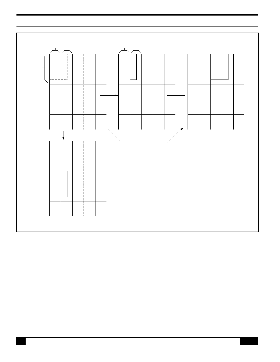
S-MOS Systems, Inc. · 2460 North First Street · San Jose, CA 95131 · Tel: (408) 922-0200 · Fax: (408) 922-0238
86
268-0.4
5.0 Display Control Functions
5.3.3
18 dots
Auto shift
Auto shift
Auto shift
Cursor address preset
8 dots
8 dots
8 dots
8 dots
Block cursor
If no text screen is displayed, only a bar cursor can be
displayed at the cursor address.
If the first layer is a mixed text and graphics screen
and the cursor shape is set to a block cursor, the
SED1330F/1335F/1336F automatically decides which
cursor shape to display. On the text screen it displays
a block cursor, and on the graphics screen, a bar
cursor.
Figure 56. Cursor movement
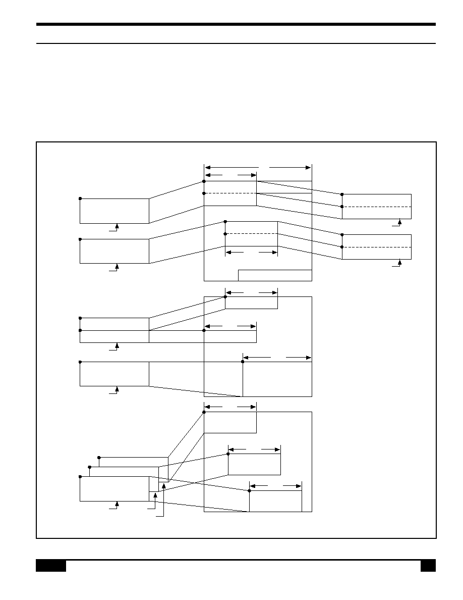
S-MOS Systems, Inc. · 2460 North First Street · San Jose, CA 95131 · Tel: (408) 922-0200 · Fax: (408) 922-0238
268-0.4
87
5.4
5.0 Display Control Functions
5.4 Memory to Display Relationship
The SED1330F/1335F/1336F supports virtual
screens that are larger than the physical size of the
LCD panel address range, C/R. A layer of the
SED1330F/1335F/1336F can be considered as a
window in the larger virtual screen held in display
memory. This window can be divided into two
blocks, with each block able to display a different
portion of the virtual screen.
This enables, for example, one block to dynamically
scroll through a data area while the other acts as a
status message display area. See Figure 49 and 50.
Graphics page 3
Display page 3
Display page 2
Display page 1
Character page 1
Character page 3
Display page 1
Display page 3
Layer 1
Layer 1
Display page 2
Character page 2
Character page 2
Display page 2
Display page 4
Layer 2
Layer 2
SAD1
SAD3
SAD2
SAD4
SAD1
SAD3
SAD2
SAD4
AP
C/R
W/S = 0
W/S = 1
C/R
CG RAM
Display page 1
Character page 1
Character page 3
Layer 1
Display page 2
Layer 2
SAD1
Graphics page 2
SAD2
SAD3
SAD3
Display page 3
SAD2
SAD1
C/R
C/R
C/R
Display page 1
Layer 1
Graphics page 2
Graphics page 1
Layer 2
Layer 3
SAD1
SAD2
SAD3
SAD3
SAD2
SAD1
C/R
C/R
C/R
Figure 57. Display layers of memory
S-MOS Systems, Inc. · 2460 North First Street · San Jose, CA 95131 · Tel: (408) 922-0200 · Fax: (408) 922-0238
88
268-0.4
5.0 Display Control Functions
5.4
Figure 58. Display window and memory
AP
CSRA
CRX
CRY
FX
SAD1
FY
L/F
Display
window
CRX
Virtual display
memory limit
0000H
FFFFH
FX = Horizontal character field
16 dots
FY = Vertical character field
16 dots
CRX = Horizontal cursor size
16 dots
CRY = Vertical cursor size
16 dots
C/R = Characters per row
240 bytes
L/F = Lines per frame
256 bytes
AP = Address pitch
64 Kbytes
S-MOS Systems, Inc. · 2460 North First Street · San Jose, CA 95131 · Tel: (408) 922-0200 · Fax: (408) 922-0238
268-0.4
89
5.4
5.0 Display Control Functions
SAD1
SAD2
SAG
0000
SL1
0300
0400
0800
SL2
2000
2800
4440
4800
4A00
F000
Character
code
Back layer
Page 1
Page 2
Page 1
Page 2
Character generator
RAM
Not used
Character generator
ROM
D7
to
D0
D7
to
D0
A (Code)
B
C
X
Y
70
88
88
88
F8
88
88
00
01110000
10001000
10001000
10001000
11111000
10001000
10001000
00000000
HEX
D7
D0
Example of character A
#4800
1
2
3
4
5
6
#4807
0080
1FFF
0000
02FF
(MSB)
D7
(LSB)(MSB)
D0 D7
Magnified image
(LSB)
D0
Display
XY
ABC
Figure 59. Memory map and magnified characters
S-MOS Systems, Inc. · 2460 North First Street · San Jose, CA 95131 · Tel: (408) 922-0200 · Fax: (408) 922-0238
90
268-0.4
5.0 Display Control Functions
5.5 5.5.1
5.5 Scrolling
The controlling microprocessor can set the SED1330F/
1335F/1336F scrolling modes by overwriting the scroll
address registers SAD1 to SAD4, and by directly
setting the scrolling mode and scrolling rate.
5.5.1 On-page Scrolling
The normal method of scrolling within a page is to
move the whole display up one line and erase the
bottom line. Since the SED1330F/1335F/1336F does
not automatically erase the bottom line, it must be
erased with blanking data when changing the scroll
address register.
ABC
WXYZ
789
WXYZ
789
ABC
WXYZ
789
WXYZ
789
Display memory
AP
C/R
Before scrolling
After scrolling
Blank
Blank
SAD1
SAD3
SAD1
Figure 60. On-page scrolling
S-MOS Systems, Inc. · 2460 North First Street · San Jose, CA 95131 · Tel: (408) 922-0200 · Fax: (408) 922-0238
268-0.4
91
5.5.2
5.0 Display Control Functions
5.5.2 Inter-page Scrolling
Scrolling between pages and page switching can be
performed only if the display memory capacity is
greater than one screen.
Figure 61. Inter-page scrolling
ABC
WXYZ
789
WXYZ
789
ABC
WXYZ
789
WXYZ
789
Display memory
AP
C/R
Before scrolling
After scrolling
SAD1
SAD1
ABC
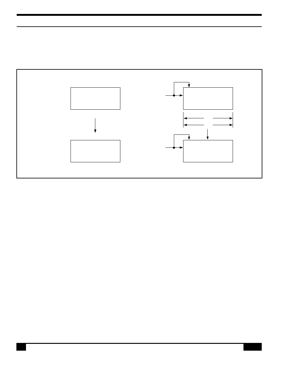
S-MOS Systems, Inc. · 2460 North First Street · San Jose, CA 95131 · Tel: (408) 922-0200 · Fax: (408) 922-0238
92
268-0.4
5.0 Display Control Functions
5.5.3
5.5.3 Horizontal Scrolling
The display can be scrolled horizontally in one-
character units, regardless of the display memory
capacity.
ABC
123
XYZ
BC
23
XYZ1
Before scrolling
After scrolling
SAD1
SAD1
Display
AP
C/R
Display memory
ABC
123
XYZ
ABC
123
XYZ
Figure 62. Horizontal wraparound scrolling
Refer to Section 9.4 for application notes.
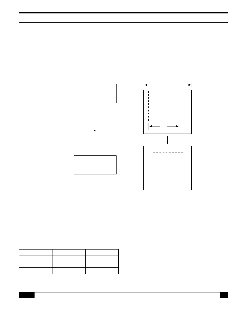
S-MOS Systems, Inc. · 2460 North First Street · San Jose, CA 95131 · Tel: (408) 922-0200 · Fax: (408) 922-0238
268-0.4
93
5.5.4 5.5.5
5.0 Display Control Functions
5.5.4 Bidirectional Scrolling
Bidirectional scrolling can be performed only if the
display memory is larger than the physical screen
both horizontally and vertically. Although scrolling is
normally done in single-character units, the HDOT
SCR command can be used to scroll horizontally in
pixel units. Single-pixel scrolling both horizontally and
vertically can be performed by using the SCROLL and
HDOT SCR commands. See Section 9.4
BC
EFG
TUV
12
Before scrolling
After scrolling
Display memory
FG
TUV
1234
56
BC
EFG
TUV
A
34
567
89
12
ABC
E FG
TUV
56 7
89
1234
AP
C/R
Figure 63. Bidirectional scrolling
5.5.5 Scroll Units
Table 21. Scroll units
Mode
Vertical
Horizontal
Text
Characters
Pixels or
characters
Graphics
Pixels
Pixels
Note that in a divided screen, each block cannot be indepen-
dently scrolled horizontally in pixel units.

S-MOS Systems, Inc. · 2460 North First Street · San Jose, CA 95131 · Tel: (408) 922-0200 · Fax: (408) 922-0238
94
268-0.4
THIS PAGE INTENTIONALLY BLANK

S-MOS Systems, Inc. · 2460 North First Street · San Jose, CA 95131 · Tel: (408) 922-0200 · Fax: (408) 922-0238
268-0.4
95
6.0
Character Generator

S-MOS Systems, Inc. · 2460 North First Street · San Jose, CA 95131 · Tel: (408) 922-0200 · Fax: (408) 922-0238
96
268-0.4
THIS PAGE INTENTIONALLY BLANK

S-MOS Systems, Inc. · 2460 North First Street · San Jose, CA 95131 · Tel: (408) 922-0200 · Fax: (408) 922-0238
268-0.4
97
6.0 6.1.3
6.0 Character Generator
6.0 Character Generator
6.1 CG Characteristics
6.1.1 Internal Character Generator
The internal character generator is recommended for
minimum system configurations containing a
SEDSED1330F/1335F/1336F, display RAM, LCD
panel, single-chip microprocessor and power supply.
Since the internal character generator uses a CMOS
mask ROM, it is also recommended for low-power
applications.
· 5
×
7-pixel font (See Section 10)
· 160 JIS standard characters
· Can be mixed with character generator RAM
(maximum of 64 CG RAM characters)
· Can be automatically spaced out up to 8
×
16
pixels
6.1.2 External Character Generator ROM
The external CG ROM can be used when fonts other
than those in the internal ROM are needed. Data is
stored in the external ROM in the same format used
in the internal ROM. (See Section 6.3.)
· Up to 8
×
8-pixel characters (M2 = 0) or 8
×
16-
pixel characters (M2 = 1)
· Up to 256 characters (192 if used together with
the internal ROM)
· Mapped into the display memory address space
at F000H to F7FFH (M2 = 0) or F000H to
FFFFH (M2 = 1)
· Characters can be up to 8
×
16-pixels; how-
ever, excess bits must be set to zero.
6.1.3 Character Generator RAM
The user can freely use the character generator RAM
for storing graphics characters. The character gen-
erator RAM can be mapped by the microprocessor
anywhere in display memory, allowing effective use of
unused address space.
· Up to 8
×
8-pixel characters (M2 = 0) or 8
×
16
characters (M2 = 1)
· Up to 256 characters if mapped at F000H to
FFFFH (64 if used together with character
generator ROM)
· Can be mapped anywhere in display memory
address space if used with the character gen-
erator ROM
· Mapped into the display memory address space
at F000H to F7FFH if not used with the charac-
ter generator ROM (more than 64 characters
are in the CG RAM). Set SAG0 to F000H and
M1 to zero when defining characters number
193 upwards.
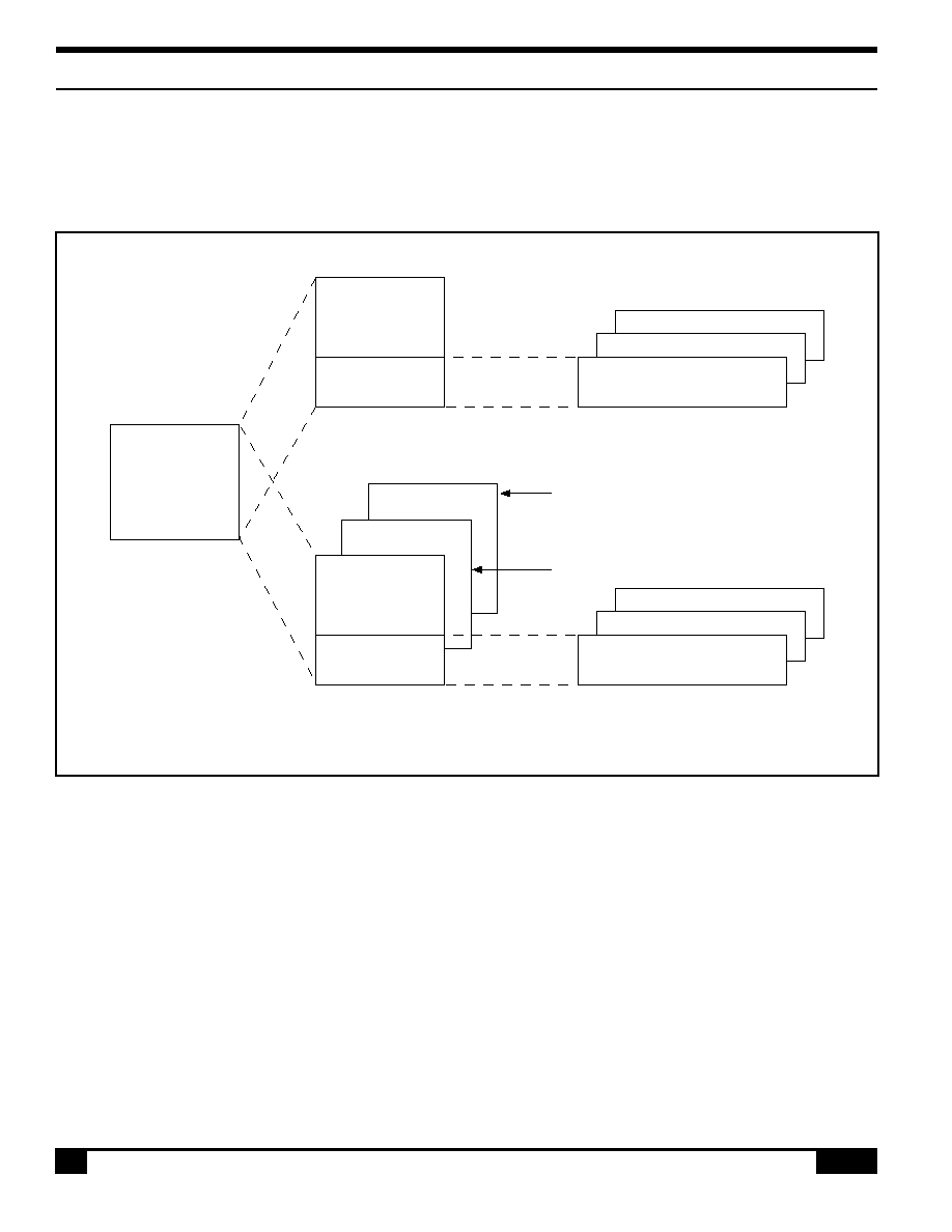
S-MOS Systems, Inc. · 2460 North First Street · San Jose, CA 95131 · Tel: (408) 922-0200 · Fax: (408) 922-0238
98
268-0.4
6.0 Character Generator
6.2
6.2 CG Memory Allocation
Since the SED1335F/1336F uses 8-bit character
codes, it can handle no more than 256 characters at
a time. However, if a wider range of characters is
required, character generator memory can be bank-
switched using the CGRAM ADR command.
Note that there can be no more than 64 characters per bank.
Figure 64. Internal and external character mapping
Builtin CG ROM
(160 characters,
5
×
7 pixels max.)
CG RAM
CG RAM 1
CG RAM 2
CG RAM n
Built-in CG ROM
(160 characters,
5
×
7 pixels max.)
CG ROM
CG RAM 1
CG RAM 2
CG RAM n
SAG
CG RAM
ADR
CG ROM
CG RAM
(64 characters max, 8
×
16 pixels max)
(64 characters max, 8
×
16 pixels max)
M0 = 1
M0 = 1
Basic CG space
(256 characters,
8
×
16 pixels max.)
256 characters max.
M1 = 0
256 characters max.
M1 = 0
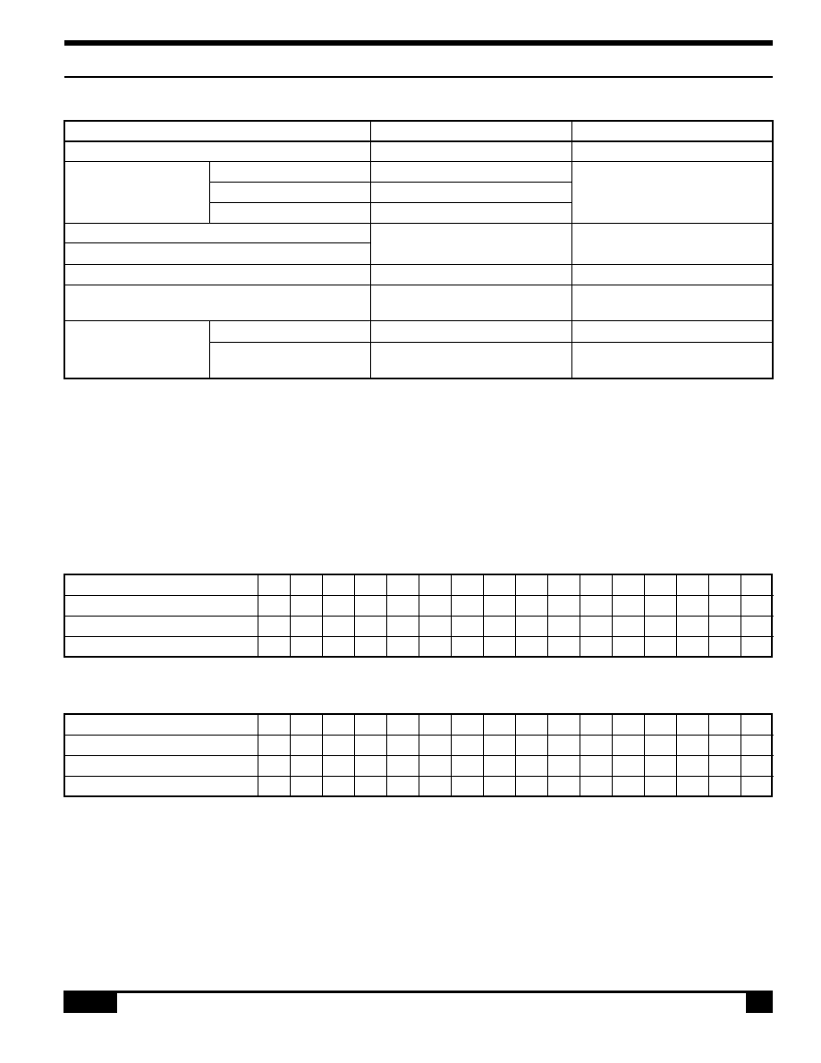
S-MOS Systems, Inc. · 2460 North First Street · San Jose, CA 95131 · Tel: (408) 922-0200 · Fax: (408) 922-0238
268-0.4
99
6.2 6.3
6.0 Character Generator
Table 22. Character mapping
Item
Parameter
Remarks
Internal/external character generator selection
M0
1 to 8 pixels
M2 = 0
Character field height
9 to 16 pixels
M2 = 1
Greater than 16 pixels
Graphics mode (8 bits
×
1 line)
Internal CG ROM/RAM select
Automatic
Determined by the
External CG ROM/RAM select
character code
CG RAM bit 6 correction
M1
CG RAM data storage address
Specified with CG RAM ADR
Can be moved anywhere in the
command
display memory address space
192 characters or less
Other than the area of Figure 58
More than 192 characters
Set SAG to F000H and overly
SAG and the CG ROM table.
External CG ROM
address
6.3 Setting the Character Generator Address
The CG RAM addresses in the VRAM address space
are not mapped directly from the address in the SAG
register. The data to be displayed is at a CG RAM
address calculated from SAG + character code +
ROW select address. This mapping is shown in Tables
23 and 24.
Table 23. Character fonts, number of lines
8 (M2 = 0, M1 = 0)
SAG
A15 A14 A13 A12 A11 A10
A9
A8
A7
A6
A5
A4
A3
A2
A1
A0
Character code
0
0
0
0
0
D7
D6
D5
D4
D3
D2
D1
D0
0
0
0
+ROW select address
0
0
0
0
0
0
0
0
0
0
0
0
0
R2
R1
R0
CG RAM address
VA15 VA14 VA13 VA12 VA11 VA10 VA9 VA8 VA7 VA6 VA5 VA4 VA3 VA2 VA1 VA0
Table 24. Character fonts, 9
number of lines
16 (M2 = 1, M1 = 0)
SAG
A15 A14 A13 A12 A11 A10
A9
A8
A7
A6
A5
A4
A3
A2
A1
A0
Character code
0
0
0
0
D7
D6
D5
D4
D3
D2
D1
D0
0
0
0
0
+ROW select address
0
0
0
0
0
0
0
0
0
0
0
0
R3
R2
R1
R0
CG RAM address
VA15 VA14 VA13 VA12 VA11 VA10 VA9 VA8 VA7 VA6 VA5 VA4 VA3 VA2 VA1 VA0
S-MOS Systems, Inc. · 2460 North First Street · San Jose, CA 95131 · Tel: (408) 922-0200 · Fax: (408) 922-0238
100
268-0.4
6.0 Character Generator
6.3 6.3.2
Row
Row 0
Row 1
Row 2
Row 7
Row 8
Row 14
Row 15
R3
0
0
0
0
1
1
1
R2
0
0
0
1
0
1
1
R1
0
0
1
1
0
1
1
R0
0
1
0
1
0
0
1
Line 1
Line 2
Figure 65. Row select address
6.3.1 M1 = 1
The SED1335F/1336F automatically converts all bits
set in bit 6 of character code for CG RAM 2 to zero.
Because of this, the CG RAM data areas become
contiguous in display memory.
When writing data to CG RAM:
· Calculate the address as for M1 = 0.
· Change bit 6 of the character code from "1" to
"0".
6.3.2 CG RAM Addressing Example
· Define a pattern for the "A" in Figure 38.
· The CG RAM table start address is 4800H.
· The character code for the defined pattern is
80H (the first character code in the CG RAM
area).
As the character code table in Figure 58 shows, codes
80H to 9FH and E0H to FFH are allocated to the CG
RAM and can be used as desired. 80H is thus the first
code for CG RAM. As characters cannot be used if
only using graphics mode, there is no need to set the
CG RAM data.
Table 25. Character data example
CGRAM ADR
5CH
Reverse the CG RAM ad-
P1
00H
dress calculation to cal-
P2
40H
culate SAG
CSRDIR
4CH
Set cursor shift direction
to right
CSRW
46H
CG RAM start address is
P1
00H
4800H
P2
48H
MWRITE
42H
P
70H
Write ROW 0 data
P2
88H
Write ROW 1 data
P3
88H
Write ROW 2 data
P4
88H
Write ROW 3 data
P5
F8H
Write ROW 4 data
P6
88H
Write ROW 5 data
P7
88H
Write ROW 6 data
P8
00H
Write ROW 7 data
P8
00H
Write ROW 8 data
P16
00H
Write ROW 15 data
Note: Lines = 1: lines in the character bitmap
8
Lines = 2: lines in the character bitmap
9
S-MOS Systems, Inc. · 2460 North First Street · San Jose, CA 95131 · Tel: (408) 922-0200 · Fax: (408) 922-0238
268-0.4
101
6.4
6.0 Character Generator
6.4 Character Codes
The following figure shows the character codes and
the codes allocated to CG RAM. All codes can be
used by the CG RAM if not using the internal ROM.
Figure 66. On-chip character codes
0
Lower 4 bits
0
1
2
3
4
5
6
7
8
9
A
B
C
D
E
F
1
2
!
"
#
$
%
&
'
(
)
*
+
,
.
-
/
3
0
1
2
3
4
5
6
7
8
9
:
;
<
+
\>
?
4
@
A
B
C
D
E
F
G
H
I
J
K
L
M
N
O
5
P
Q
R
S
T
U
V
W
X
Y
Z
[
¥
]
^
_
6
'
a
b
c
d
e
f
g
h
i
j
k
l
m
n
o
7
p
q
r
s
t
u
v
w
x
y
z
{
|
}
8
Upper 4 bits
8
A
B
C
D
E
F

S-MOS Systems, Inc. · 2460 North First Street · San Jose, CA 95131 · Tel: (408) 922-0200 · Fax: (408) 922-0238
102
268-0.4
THIS PAGE INTENTIONALLY BLANK

S-MOS Systems, Inc. · 2460 North First Street · San Jose, CA 95131 · Tel: (408) 922-0200 · Fax: (408) 922-0238
268-0.4
103
7.0
TV Mode
(SED1336F only)

S-MOS Systems, Inc. · 2460 North First Street · San Jose, CA 95131 · Tel: (408) 922-0200 · Fax: (408) 922-0238
104
268-0.4
THIS PAGE INTENTIONALLY BLANK
S-MOS Systems, Inc. · 2460 North First Street · San Jose, CA 95131 · Tel: (408) 922-0200 · Fax: (408) 922-0238
268-0.4
105
7.0 7.1
7.0 TV Mode (SED1336F only)
7.0 TV Mode (SED1336F only)
When used with an external video mixer circuit, the
SED1336F can show the same display on a television
as on the LCD panel. In addition, the changeover from
LCD-only to TV-and-LCD display is instantaneous
with the changing of the T/L register using the System
Set instruction.
The TV and LCD display register parameters which
are determined by hardware constraints are shown in
Table 26.
Table 26. Register parameters
Clock Cycles
Oscillator
System
TC/R (Hex)
C/R (Hex)
L/F (Hex)
per
Frequency,
T/L
Horizontal Line
f
O
(MHz)
NTSC
2A
1F
C7
388
6.1050
1
PAL
2A
1F
C7
388
6.0625
1
LCD
2A
1F
C7
388
6.0625 or
0
6.1050
7.1 Sync Generator Circuit Timing
The NTSC and PAL vertical sync signal waveforms
are shown in Figure 59 and 60, respectively. The
vertical sync timing parameters and VSD output states
are shown in Table 27.
Interval after
equalizing pulses
21H
Color field I vertical blanking interval
11H
3H
3H
3H
21H
Pre-blanking
interval
Start of
field I
1.5 ± 0.1µs
2
1
4
3
5
6
7
8
9
10
19
20
H
H
H
9-line vertical interval
H
T
I
0.5H
Vertical serration
pulse interval
Equalizing
pulse interval
Horizontal
sync interval
Display
interval
Interval before
equalizing pulses
Vertical Sync
pulse interval
Display
interval
Reference
subcarrier phase
color field I
Post-
blanking
interval
Figure 67. NTSC vertical sync waveform
S-MOS Systems, Inc. · 2460 North First Street · San Jose, CA 95131 · Tel: (408) 922-0200 · Fax: (408) 922-0238
106
268-0.4
7.0 TV Mode (SED1336 only)
7.1
42H
2.5H
2.5H
Field blanking (25H + a) (a = 11-line blanking interval)
17.5H
45H
2.5H
311
Interval after
equalizing pulses
Interval before
equalizing pulses
Vertical sync
pulse interval
Display
interval
Reference
subcarrier phase
color field I
Post-
blanking
interval
Pre-blanking
interval
Display
period
312
313
314
315
316
317
318
319
320
335
Figure 68. PAL vertical sync waveform
Table 27. Vertical sync timing characteristics
Pre-
Interval
Vertical
Interval
Reference
Post-
Equalizing
Vertical
Parameter
blanking
before
Sync Pulse
after
Subcarrier
blanking
Display
Pulse
Serration
Interval
Equalizing
Interval
Equalizing Phase Color
Interval
Interval
Interval
Pulse
Pulse
Pulse
Field I
Interval
NTSC
system
21H
3H
3H
3H
11H
21H
200H
15CK
27CK
timing
PAL
system
42H
2.5H
2.5H
2.5H
17.5H
45H
200H
15CK
27CK
timing
VSD
High
High
LOW or
output
impedance
LOW
LOW
LOW
LOW
impedance
high
--
--
level
impedance
Notes:
1. The NTSC system uses 262 lines per screen, and the PAL system, 312.
2. H = Horizontal line period
CK = Oscillator period
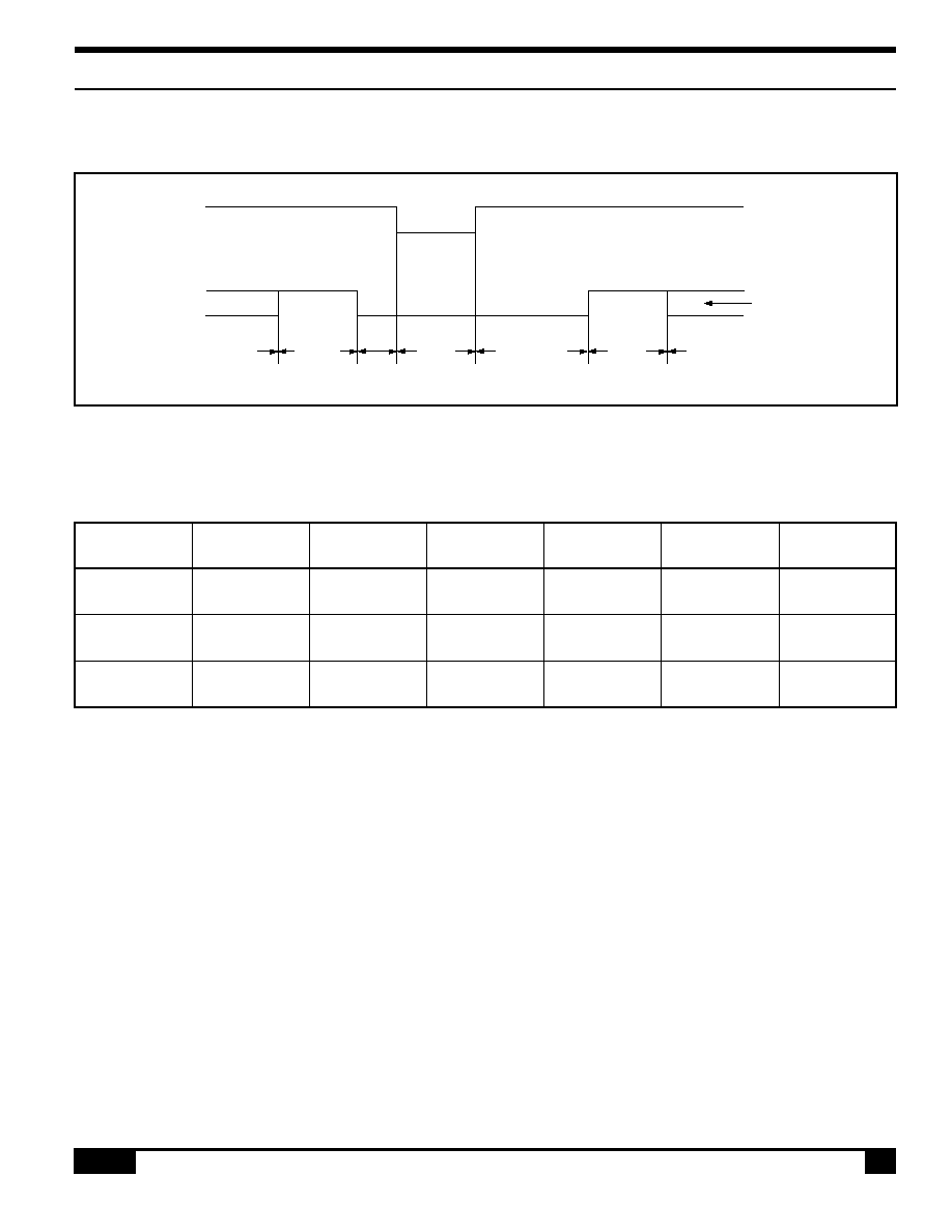
S-MOS Systems, Inc. · 2460 North First Street · San Jose, CA 95131 · Tel: (408) 922-0200 · Fax: (408) 922-0238
268-0.4
107
7.1
7.0 TV Mode (SED1336 only)
The horizontal sync signal waveforms are shown in
Figure 61, and the timing parameters and VSD output
states, in Table 28. Note that SNC and VSD are both
high-impedance when in LCD mode.
Pre-
blanking
interval
Horizontal
sync
pulse
Post-
blanking
interval
Display
interval
Display
interval
Front
porch
Back porch
High
impedance
High
impedance
High
impedance
Low or high
impedance
SNC
VSD
Figure 69. Horizontal sync waveforms
Table 28. Horizontal sync characteristics
Parameter
Pre-blanking
Front Porch
Horizontal
Back Porch
Post-blanking
Display
Interval
Sync Pulse
Interval
Interval
NTSC
29CK
10CK
29CK
28CK
36CK
256CK
system timing
PAL
29CK
10CK
29CK
34CK
30CK
256CK
system timing
VSD
High
LOW
LOW
LOW
High
LOW or High
output level
impedance
impedance
impedance

S-MOS Systems, Inc. · 2460 North First Street · San Jose, CA 95131 · Tel: (408) 922-0200 · Fax: (408) 922-0238
108
268-0.4
THIS PAGE INTENTIONALLY BLANK

S-MOS Systems, Inc. · 2460 North First Street · San Jose, CA 95131 · Tel: (408) 922-0200 · Fax: (408) 922-0238
268-0.4
109
8.0
Description of Circuit Blocks

S-MOS Systems, Inc. · 2460 North First Street · San Jose, CA 95131 · Tel: (408) 922-0200 · Fax: (408) 922-0238
110
268-0.4
THIS PAGE INTENTIONALLY BLANK
S-MOS Systems, Inc. · 2460 North First Street · San Jose, CA 95131 · Tel: (408) 922-0200 · Fax: (408) 922-0238
268-0.4
111
8.0 8.1.2.3
8.0 Description of Circuit Blocks
8.0 Description of Circuit Blocks
8.1 Microprocessor Interface
8.1.1 System Bus Interface
SEL1, SEL2 (SED1330F and SED1335F only), A0,
RD, WR and CS are used as control signals for the
microprocessor data bus. A0 is normally connected to
the lowest bit of the system address bus. SEL1 and
SEL2 change the operation of the RD and WR pins to
enable interfacing to either an 8080 or 6800 family
bus, and should have either a pull-up or a pull-down
resistor.
With microprocessors using an 8080 family interface,
the SED1330F/1335F/1336F is normally mapped into
the I/O address space.
8.1.1.1 8080 series
Table 29. 8080 series interface signals
A0 RD WR
Function
0
0
1
Status flag read
1
0
1
Display data and cursor address
read
0
1
0
Display data and parameter write
1
1
0
Command write
8.1.1.2 6800 series
Table 30. 6800 series interface signals
A0 RD WR
Function
0
1
1
Status flag read
1
1
1
Display data and cursor address
read
0
0
1
Display data and parameter write
1
0
1
Command write
8.1.2 Microprocessor Synchronization
The SED1330F/1335F/1336F interface operates at
full bus speed, completing the execution of each
command within the cycle time, t
CYC
. The controlling
micro-processor's performance is thus not hampered
by polling or handshaking when accessing the
SED1330F/1335F/1336F.
Display flicker may occur if there is more than one
consecutive access that cannot be ignored within a
frame. The microprocessor can minimize this either
by performing these accesses intermittently, or by
continuously checking the status flag (D6) and waiting
for it to become HIGH.
8.1.2.1 Display Status Indication Output
(For SED1336 only)
When CS, A0 and RD are LOW, D6 functions as the
display status indication output. It is HIGH during the
TV-mode vertical retrace period or the LCD-mode
horizontal retrace period, and LOW, during the period
the controller is writing to the display. By monitoring
D6 and writing to the data memory only during retrace
periods, the display can be updated without causing
screen flicker.
8.1.2.2 Internal Register Access
The SYSTEM SET and SLEEP IN commands can be
used to perform input/output to the SED1330F/1335F/
1336F independently of the system clock frequency.
These are the only commands that can be used while
the SED1330F/1335F/1336F is in sleep mode.
8.1.2.3 Display Memory Access
The SED1330F/1335F/1336F supports a form of
pipelined processing, in which the microprocessor
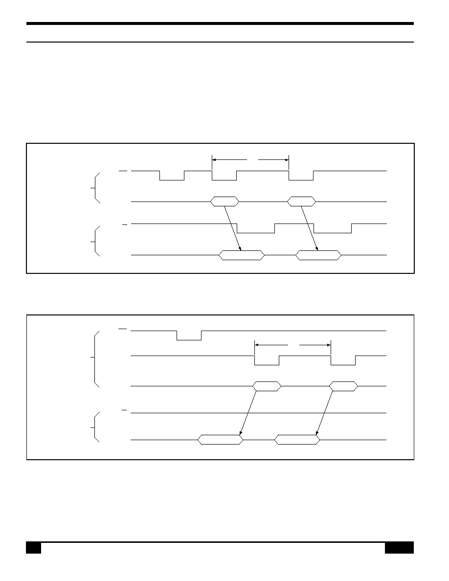
S-MOS Systems, Inc. · 2460 North First Street · San Jose, CA 95131 · Tel: (408) 922-0200 · Fax: (408) 922-0238
112
268-0.4
8.0 Description of Circuit Blocks
8.1.2.3
synchronizes its processing to the SED1330F/1335F/
1336F's timing. When writing, the microprocessor
first issues the MWRITE command. It then repeatedly
writes display data to the SED1336F using the sys-
tem bus timing. This ensures that the microprocessor
is not slowed down even if the display memory
access times are slower than the system bus access
times. See Figure 70.
When reading, the microprocessor first issues the
MREAD command, which causes the SED1330F/
1335F/1336F to load the first read data into its output
buffer. The microprocessor then reads data from the
SED1330F/1335F/1336F using the system bus tim-
ing. With each read, the SED1330F/1335F/1336F
reads the next data item from the display memory
ready for the next read access. See Figure 71.
Figure 70. Display memory write cycle
Figure 71. Display memory read cycle
Note: A possible problem with the display memory read cycle is that the system bus access time, t
ACC
, does not depend on the display
memory access time, t
ACV
. The microprocessor may only make repeated reads if the read loop time exceeds the SED1330F/
1335F/1336F cycle time, t
CYC
. If it does not, NOP instructions may be inserted in the program loop. t
ACC
, t
ACV
and t
CYC
limits
are given in Section 4.3.
WR
D0 to D7
WR/W
VD0 to VD7
t
CYC
Command write
Data write
Data write
Microprocessor
Display memory
t
CYC
Command write
Data read
Data read
WR
RD
D0 to D7
WR/W
VD0 to VD7
Microprocessor
Display memory
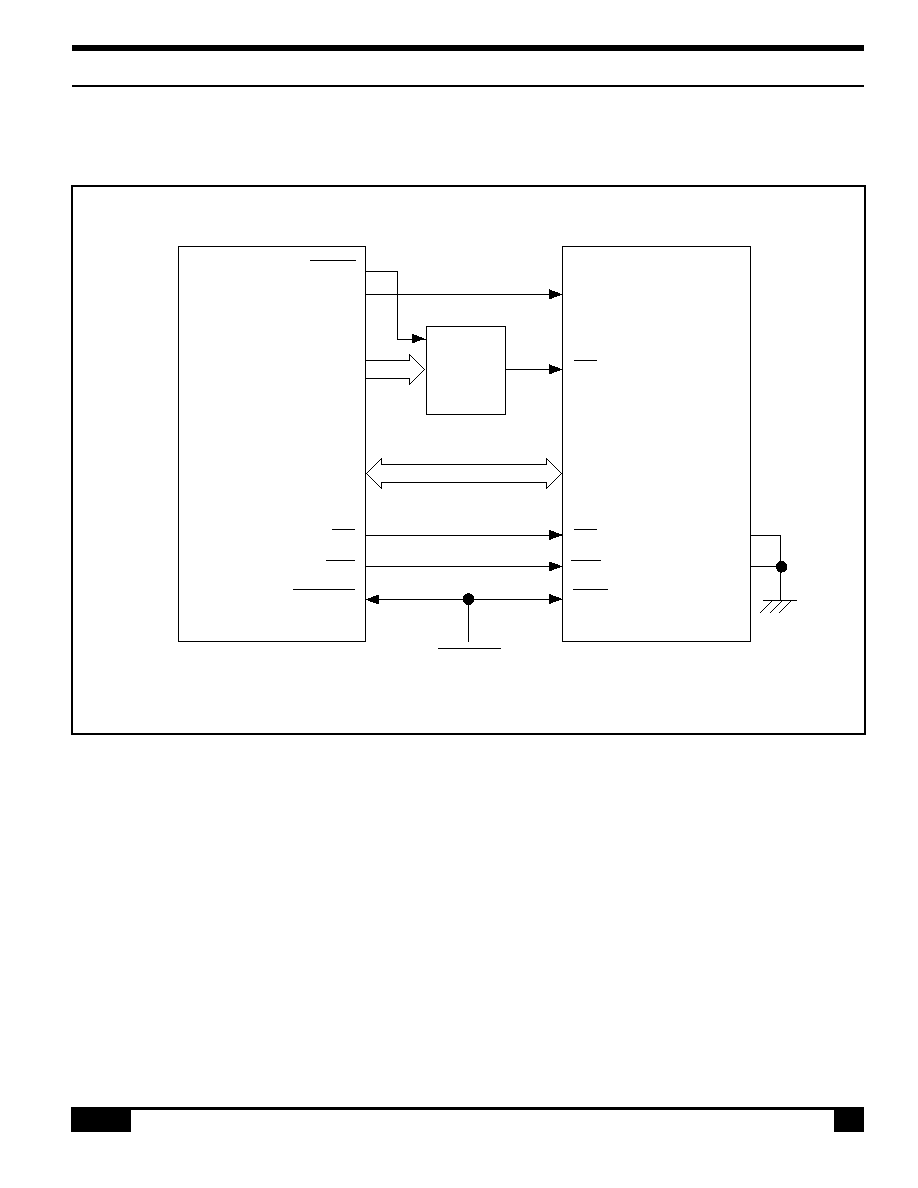
S-MOS Systems, Inc. · 2460 North First Street · San Jose, CA 95131 · Tel: (408) 922-0200 · Fax: (408) 922-0238
268-0.4
113
8.1.3 8.1.3.1
8.0 Description of Circuit Blocks
8.1.3 Interface Examples
8.1.3.1 Z80® to SED1330F/1335F/1336F Interface
Note: Z80® is a registered trademark of Zilog Corporation.
Figure 72. Z80® to SED1330F/1335F/1336F* interface
RESET
Z80
®
Decoder
IORQ
SED1335F/
1336F
SEL 1
SEL 2
A0
A1
to
A15
D0
to
D7
RD
WR
RESET
A0
CS
D0
to
D7
RD
WR
RES
Note: *For SED1336F: SEL 2 is open..
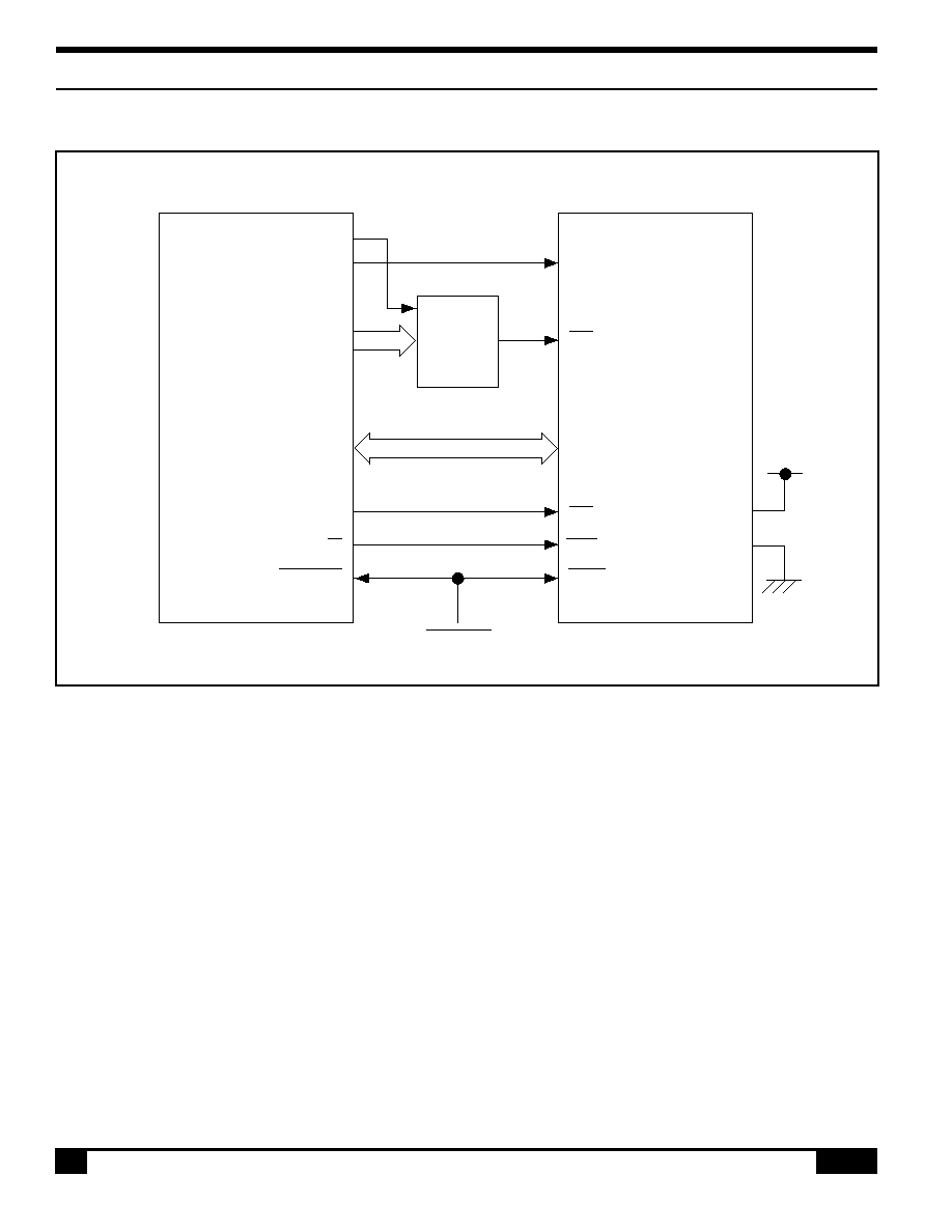
S-MOS Systems, Inc. · 2460 North First Street · San Jose, CA 95131 · Tel: (408) 922-0200 · Fax: (408) 922-0238
114
268-0.4
8.1.3.2 6802 to SED1330F/1335F/1336F Interface
Figure 73. 6802 to SED1330F/1335F/1336F interface
8.0 Description of Circuit Blocks
8.1.3.2
RESET
6802
Decoder
A0
CS
D0
to
D7
RD
WR
RES
VMA
V
DD
SED1335F/
1336F
SEL 1
SEL 2
A0
A1
to
A15
D0
to
D7
E
R/W
RESET
Note: *For SED1336F: SEL 2 is open..
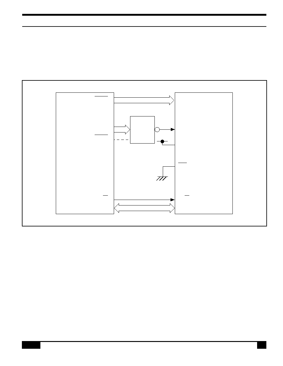
S-MOS Systems, Inc. · 2460 North First Street · San Jose, CA 95131 · Tel: (408) 922-0200 · Fax: (408) 922-0238
268-0.4
115
8.2 8.2.2
8.0 Description of Circuit Blocks
8.2 Display Memory Interface
8.2.1 Static RAM
The figure below shows the interface between an 8K
×
8 static RAM and the SED1330F/1335F/1336F.
HC138
V
DD
SED1335F/
1336F
6264 SRAM
A0 to A12
CE1
CE2
OE
R/W
I/O1 to I/O8
VA0 to VA12
VA13 to VA15
VCE
VR/W
I/O1 to I/O8
Y
A
to
C
Figure 74. Static RAM interface
8.2.2 Supply Current during Display Memory Access
The 24 address and data lines of the SED1330F/
1335F/1336F cycle at one-third of the oscillator fre-
quency, f
OSC
. The charge and discharge current on
these pins, I
VOP
, is given by the equation below.
When I
VOP
exceeds I
OPR
, it can be estimated by:
I
VOP
C V f
where C is the capacitance of the display memory
bus, V is the operating voltage, and f is the operating
frequency.
If V
OPR
= 5.0V, f = 1.0 MHz, and the display memory
bus capacitance is 1.0 pF per line:
I
VOP
120
µ
A / MHz
×
pF
To reduce current flow during display memory ac-
cesses, it is important to use low-power memory, and
to minimize both the number of devices and the
parasitic capacitance.
Note that bus buffers are required if the bus is heavily
loaded.
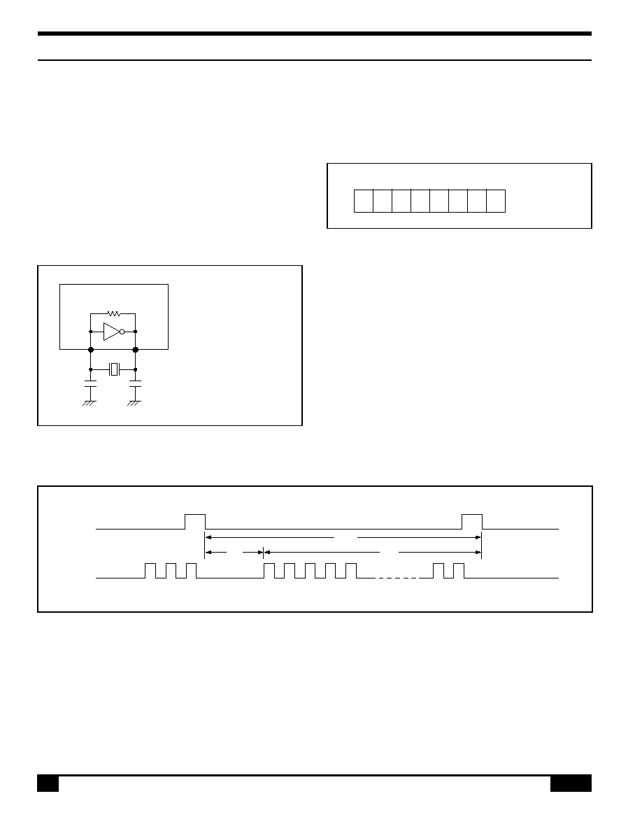
S-MOS Systems, Inc. · 2460 North First Street · San Jose, CA 95131 · Tel: (408) 922-0200 · Fax: (408) 922-0238
116
268-0.4
8.0 Description of Circuit Blocks
8.3 8.4
8.3 Oscillator Circuit
The SED1330F/1335F/1336F incorporates an oscil-
lator circuit. A stable oscillator can be constructed
simply by connecting an AT-cut crystal and two ca-
pacitors to OSC1 and OSC2, as shown in the figure
below. If the oscillator frequency is increased, C
D
and
C
G
should be decreased proportionally.
Note that the circuit board lines to OSC1 and OSC2
must be as short as possible to prevent wiring capaci-
tance from changing the oscillator frequency or in-
creasing the power consumption.
Figure 75. Crystal oscillator
8.4 Status Flag
The SED1330F/1335F/1336F has a single bit status
flag.
D6: X line standby
t
m
t
TC/R
LP
XSCL
t
C/R
Figure 77. C/R to TC/R time difference
SED1335F/1336F
OSC2
OSC1
C
D
C
G
C
D
= 3 to 20 pF
C
G
= 2 to 18 pF
Load impedance = 700
(max)
Figure 76. Status flag
The D6 status flag is LOW (0) for the TC/R - C/R cycles
at the end of each line where the SED1330F/1335F/
1336F is not reading the display memory. The micro-
processor may use this period to update display
memory without affecting the display; however, it is
recommended that the display be turned off when
refreshing the whole display.
D7
D0
X
D6
X
X
X
X
X
X
X: Don't care
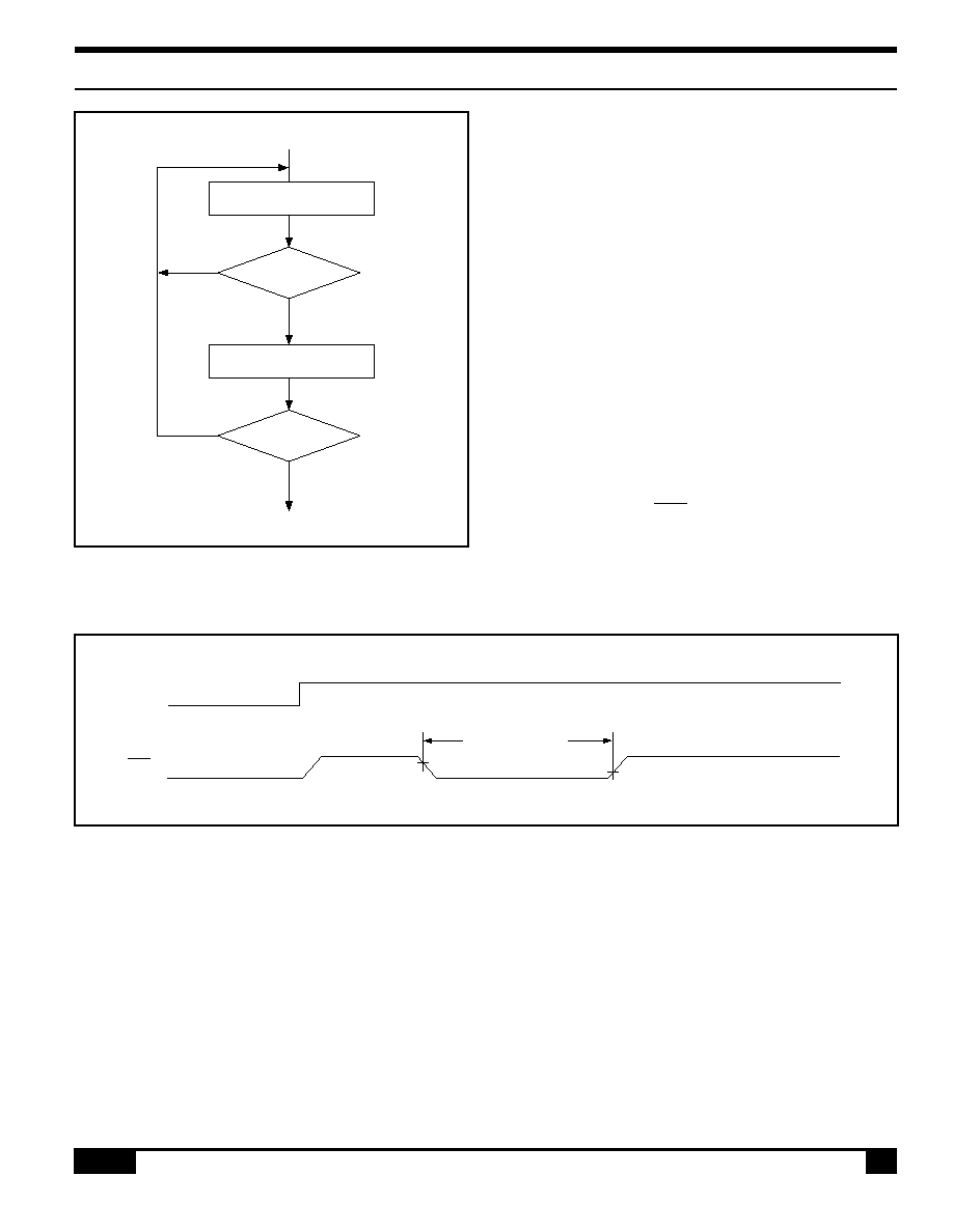
S-MOS Systems, Inc. · 2460 North First Street · San Jose, CA 95131 · Tel: (408) 922-0200 · Fax: (408) 922-0238
268-0.4
117
8.4 8.5
8.0 Description of Circuit Blocks
Figure 78. Flowchart for busy flag checking
8.5 Reset
The SED1330F requires a reset pulse at least 1 ms
long after power-on in order to re-initialize its internal
state. The SED1335F/1336F requires a minimum
reset pulse of 200
µ
s.
During reset, the LCD drive signals XD, LP and FR are
halted.
For maximum reliability, it is not recommended to
apply a DC voltage to the LCD panel while the
SED1330F/1335F/1336F is reset. Turn off the LCD
power supplies for at least one frame period after the
start of the reset pulse.
The SED1330F/1335F/1336F cannot receive com-
mands while it is reset. Commands to initialize the
internal registers should be issued soon after a reset.
A delay of 3 ms (maximum) is required following the
rising edges of both RES and V
DD
to allow for system
stabilization.
200µs reset pulse
0.7 V
DD
0.3 V
DD
V
DD
RES
Figure 79. Reset timing
Read Status Flag
D6 = 1?
Data Input
Data Input ?
No
No
Yes
Yes

S-MOS Systems, Inc. · 2460 North First Street · San Jose, CA 95131 · Tel: (408) 922-0200 · Fax: (408) 922-0238
118
268-0.4
THIS PAGE INTENTIONALLY BLANK

S-MOS Systems, Inc. · 2460 North First Street · San Jose, CA 95131 · Tel: (408) 922-0200 · Fax: (408) 922-0238
268-0.4
119
9.0
Application Notes

S-MOS Systems, Inc. · 2460 North First Street · San Jose, CA 95131 · Tel: (408) 922-0200 · Fax: (408) 922-0238
120
268-0.4
THIS PAGE INTENTIONALLY BLANK
S-MOS Systems, Inc. · 2460 North First Street · San Jose, CA 95131 · Tel: (408) 922-0200 · Fax: (408) 922-0238
268-0.4
121
9.0 9.1.1
9.0 Application Notes
9.0 Application Notes
9.1 Initialization Parameters
The parameters for the initialization commands must
be determined first. Square brackets around a param-
eter name indicate the number represented by the
parameter, rather than the value written to the param-
eter register. For example, [FX] = FX + 1.
9.1.1
SYSTEM SET Instruction and Param-
eters
· FX
The horizontal character field size is deter-
mined from the horizontal display size in pixels
[VD] and the number of characters per line
[VC].
[VD] / [VC]
[FX]
VD: # of X-directional dots
VC: # of X-directional characters
· C/R
C/R can be determined from VC and FX.
[C/R] = RND([FX] / 8)
×
[VC]
where RND(x) denotes x rounded up to the
next highest integer. [C/R] is the number of
bytes per line, not the number of characters.
· TC/R
TC/R must satisfy the condition [TC/R]
[C/R]
+ 4.
· f
OSC
and f
FR
Once TC/R has been set, the frame frequency,
f
FR
, and lines per frame [L/F] will also have
been set. The lower limit on the oscillator
frequency f
OSC
is given by:
f
OSC
([TC/R]
×
9 + 1)
×
[L/F]
×
f
FR
· If no standard crystal close to the calculated
value of f
OSC
exists, a higher frequency crystal
can be used and the value of TC/R revised
using the above equation.
· Symptoms of an incorrect TC/R setting are
listed below. If any of these appears, check the
value of TC/R and modify it if necessary.
· Vertical scanning halts and a high-con-
trast horizontal line appears.
· All pixels are on or off.
· The LP output signal is absent or cor-
rupted.
· The display is unstable.
Table 31. Epson LCD unit example parameters (SED1335F only)
Resolution (X
×
Y)
[FX]
[FY]
[C/R]
TC/R
f
OSC
(MHz)
See Note 2
[FX] = 6 pixels:
8 or 16, depending
[C/R] = 42 = 2AH bytes:
256
×
64
256 / 6 = 42 remainder 4
on the screen
C/R = 29H. When using HDOT
2DH
1.85
= 4 blank pixels
SCR, [C/R] = 43 bytes
[FX] = 6 pixels:
8 or 16, depending
[C/R] = 85 = 55H bytes:
512
×
64
512 / 6 = 85 remainder 2
on the screen
C/R = 54H. When using HDOT
58H
3.59
= 2 blank pixels
SCR, [C/R] = 86 bytes
[FX] = 8 pixels:
8 or 16, depending
[C/R] = 32 = 20H bytes:
256
×
128
256 / 8 = 32 remainder 0
on the screen
C/R = 19H. When using HDOT
22H
2.90
= no blank pixels
SCR, [C/R] = 33 bytes
[FX] = 10 pixels:
8 or 16, depending
[C/R] = 102 = 66H bytes:
512
×
128
512 / 10 = 51 remainder
on the screen
C/R = 65H. When using HDOT
69H
8.55
2 = 2 blank pixels
SCR, [C/R] = 103 bytes
Notes:
1. The remainder pixels on the right-hand side of the display are automatically blanked by the SED1335F. There is no need to
zero the display memory corresponding to these pixels.
2. Assuming a frame frequency of 60 Hz.
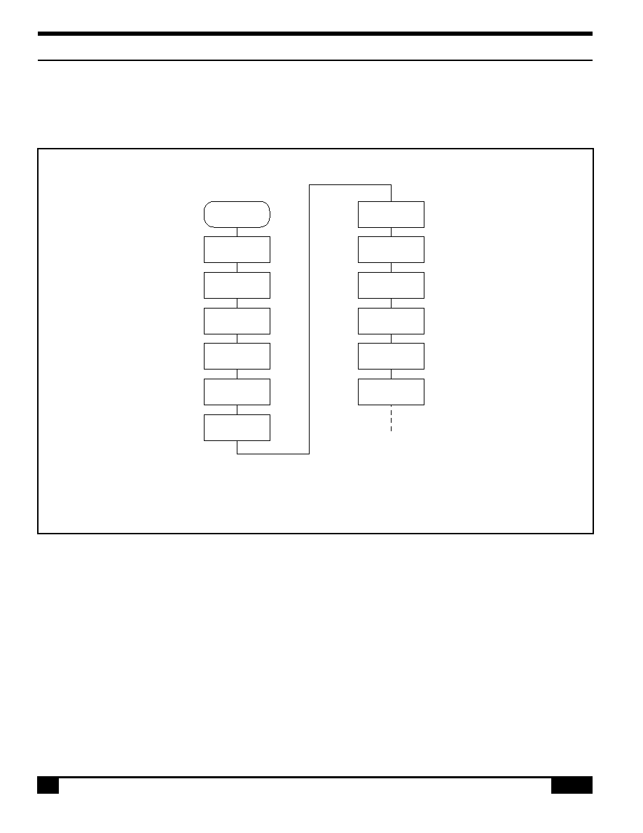
S-MOS Systems, Inc. · 2460 North First Street · San Jose, CA 95131 · Tel: (408) 922-0200 · Fax: (408) 922-0238
122
268-0.4
9.0 Application Notes
9.1.2
9.1.2 Initialization Example
The initialization example shown in Figure 80 is for a
SED1330F/1335F/1336F with an 8-bit microproces-
sor interface bus display unit (512
×
128 pixels).
Start
Clear first
memory layer
Supply on
SYSTEM SET
SCROLL
HDOT SCR
OVLAY
DISP OFF
Clear second
memory layer
Output display
data
CSRW
CSR FORM
DISP ON
Note: Set the cursor address to the start of each screen's layer memory, and use MWRITE to fill the memory with space
characters, 20H (text screen only) or 00H (graphics screen only). Determining which memory to clear is explained in section
9.1.3.
Figure 80. Initialization procedure
S-MOS Systems, Inc. · 2460 North First Street · San Jose, CA 95131 · Tel: (408) 922-0200 · Fax: (408) 922-0238
268-0.4
123
9.1.2
9.0 Application Notes
Table 32. Initialization procedure
No.
Command
Operation
1
Power-up
2
Supply
Wait for at least 3 ms after reset with V
DD
4.5V
3
SYSTEM SET
initialization.
C = 40H
P1 = 38H
M0: Internal CG ROM
M1: CG RAM is 32 characters maximum
M2: 8 lines per character
W/S: Two-panel drive
IV: No top-line compensation
P2 = 87H
FX: Horizontal character size = 8 pixels
WF: Two-frame AC drive
P3 = 07H
FY: Vertical character size = 8 pixels
P4 = 3FH
C/R: 64 display addresses per line
P5 = 49H
TC/R: Total address range per line = 90
f
OSC
= 6.0 MHz, f
FR
= 70 Hz
P6 = 7FH
L/F: 128 display lines
P7 = 80H
AP: Virtual screen horizontal size is 128 addresses
P8 = 00H
4
SCROLL
C = 44H
P1 = 00H
First screen block start address
P2 = 00H
Set to 0000H
P3 = 40H
Display lines in first screen block = 64
P4 = 00H
Second screen block start address
P5 = 10H
Set to 1000H
P6 = 40H
Display lines in second screen block = 64
P7 = 00H
Third screen block start address
P8 = 04H
Set to 0400H
(continued)
S-MOS Systems, Inc. · 2460 North First Street · San Jose, CA 95131 · Tel: (408) 922-0200 · Fax: (408) 922-0238
124
268-0.4
5
HDOT SCR
C = 5AH
P1 = 00H
Set horizontal pixel shift to zero
6
OVLAY
C = 5BH
P1 = 01H
MX 1, MX 0: Inverse video superposition
DM 1: First screen block is text mode
DM 2: Third screen block is text mode
7
DISP ON/OFF
C = 58H
D: Display OFF
P1 = 56H
FC1, FC0: Flash cursor at 2 Hz
FP1, FP0: First screen block ON
FP3, FP2: Second and fourth screen blocks ON
FP5, FP4: Third screen block ON
8
Clear data in first layer
Fill first screen layer memory with 20H (space character)
(continued)
9.0 Application Notes
9.1.2
Table 32. Initialization procedure (continued)
No.
Command
Operation
P9 = 00H
Fourth screen block start address
P10 = 30H
Set to 3000H
Display memory
1st display memory page
2nd display memory page
3rd display memory page
4th display memory page
(SAD1) 0000H
(SAD3) 0400H
0800H
(SAD2) 1000H
(SAD4) 3000H
5000H
S-MOS Systems, Inc. · 2460 North First Street · San Jose, CA 95131 · Tel: (408) 922-0200 · Fax: (408) 922-0238
268-0.4
125
13
CSR DIR
C = 4CH
Set cursor shift direction to right
(continued)
9.1.2
9.0 Application Notes
Table 32. Initialization procedure (continued)
No.
Command
Operation
9
Clear data in second layer
Fill second screen layer memory with 00H (blank data)
Display
1st layer
2nd layer
Blank code in every position
Character code in every position
10
CSRW
C = 46H
P1 = 00H
Set cursor to start of first screen block
P2 = 00H
11
CSR FORM
C = 5DH
P1 = 04H
CRX: Horizontal cursor size = 5 pixels
P2 = 86H
CRY: Vertical cursor size = 7 pixels
CM: Block cursor
12
DISP ON/OFF
C = 59H
Display ON
Display
S-MOS Systems, Inc. · 2460 North First Street · San Jose, CA 95131 · Tel: (408) 922-0200 · Fax: (408) 922-0238
126
268-0.4
18
CSRW
C = 46H
P1 = 01H
Set cursor address to 1001H
P2 = 10H
19
MWRITE
C = 42H
(continued)
9.0 Application Notes
9.1.2
Table 32. Initialization procedure (continued)
No.
Command
Operation
14
MWRITE
C = 42H
P1 = 20H
` '
P2 = 45H
`E'
P3 = 50H
`P'
P4 = 53H
`S'
P5 = 4FH
`O'
P6 = 4EH
`N'
15
CSRW
C = 46H
P1 = 00H
Set cursor to start of second screen block
P2 = 10H
16
CSR DIR
C = 4FH
Set cursor shift direction to down
17
MWRITE
C = 42H
P1 = FFH
Fill in a square to the left of the `E'
P9 = FFH
EPSON
EPSON
S-MOS Systems, Inc. · 2460 North First Street · San Jose, CA 95131 · Tel: (408) 922-0200 · Fax: (408) 922-0238
268-0.4
127
30
CSRW
C = 46H
P1 = 00H
Set cursor to line three of the first screen block
P2 = 01H
31
CSR DIR
C = 4CH
Set cursor shift direction to right
32
MWRITE
C = 42H
P1 = 44H
`D'
P2 = 6FH
`o'
P3 = 74H
`t'
P4 = 20H
` '
P5 = 4DH
`M'
P6 = 61H
`a'
P7 = 74H
`t'
P8 = 72H
`r'
P9 = 69H
`i'
P10 = 78H
`x'
P11 = 20H
` '
P12 = 4CH
`L'
P13 = 43H
`C'
P14 = 44H
`D'
9.1.2
9.0 Application Notes
Table 32. Initialization procedure (continued)
No.
Command
Operation
P1 = FFH
Fill in the second screen block in the second column of line
1
P9 = FFH
20
CSRW
Repeat operations 18 and 19 to fill in the background under
`EPSON'
29
MWRITE
EPSON
Inverse display
EPSON
Inverse display
Dot matrix LCD
S-MOS Systems, Inc. · 2460 North First Street · San Jose, CA 95131 · Tel: (408) 922-0200 · Fax: (408) 922-0238
128
268-0.4
9.0 Application Notes
9.1.3
9.1.3 Display Mode Setting Example 1: Combining Text and Graphics
· Conditions
· 320
×
200 pixels, single-panel drive (1/
200 duty cycle)
· First layer: text display
· Second layer: graphics display
· 8
×
8-pixel character font
· CG RAM not required
· Display memory allocation
· First layer (text): 320/8 = 40 characters
per line, 200/8 = 25 lines. Required
memory size = 40
×
25 = 1000 bytes.
· Second layer (graphics): 320/8 = 40 char-
acters per line, 200/1 = 200 lines. Re-
quired memory size = 40
×
200 = 8000
bytes.
03E8H
2nd graphics layer
(8000 bytes)
2327H
0000H
1st character layer
(1000 bytes)
03E7H
Figure 81. Character over graphics layers
· Register setup procedure
SYSTEM SET
TC/R calculation
C =
40H
P1 =
30H
f
OSC
= 6 MHz
P2 =
87H
f
FR
= 70 Hz
P3 =
07H
P4 =
27H
(1/6)
×
9
×
[TC/R]
×
200 = 1/70
P5 =
2FH
[TC/R] = 48, so TC/R = 2FH
P6 =
C7H
P7 =
28H
P8 =
00H
SCROLL
C =
44H
P1 =
00H
P2 =
00H
P3 =
C8H
P4 =
E8H
P5 =
03H
P6 =
C8H
P7 =
XH
P8 =
XH
P9 =
XH
P10 =
XH
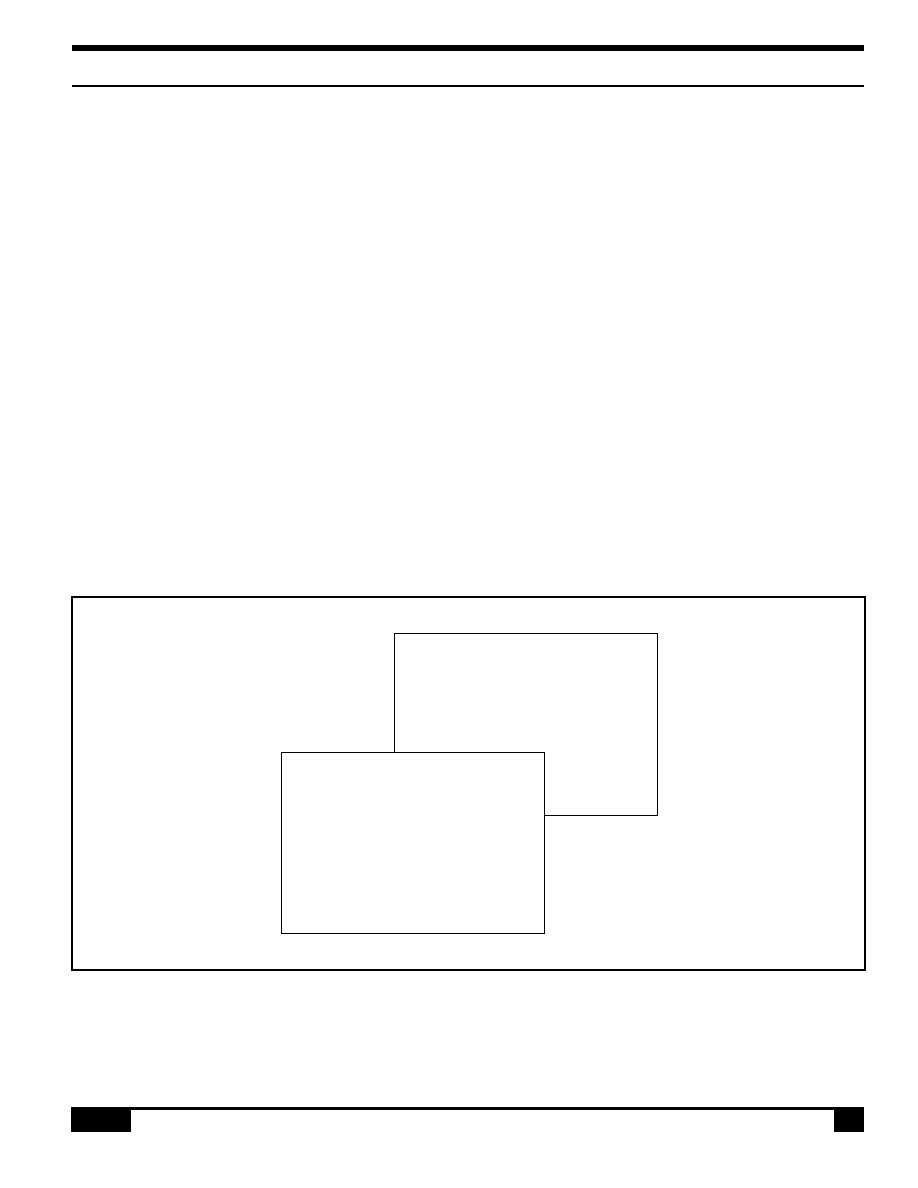
S-MOS Systems, Inc. · 2460 North First Street · San Jose, CA 95131 · Tel: (408) 922-0200 · Fax: (408) 922-0238
268-0.4
129
9.1.3 9.1.4
9.0 Application Notes
CSR FORM
C =
5DH
P1 =
04H
P2 =
86H
HDOT SCR
C =
5AH
P1 =
00H
OVLAY
C =
5BH
P1 =
00H
DISP ON/OFF
C =
59H
P1 =
16H
X = Don't care
9.1.4 Display Mode Setting Example 2: Combining Graphics and Graphics
· Conditions
· 320
×
200 pixels, single-panel drive (1/
200 duty cycle)
· First layer: graphics display
· Second layer: graphics display
· Display memory allocation
· First layer (graphics): 320/8 = 40 charac-
ters per line, 200/1 = 200 lines. Required
memory size = 40
×
200 = 8000 bytes.
· Second layer (graphics): 320/8 = 40 char-
acters per line, 200/1 = 200 lines. Re-
quired memory size = 8000 bytes.
Figure 82. Two-layer graphics
1F40H
2nd graphics layer
(8000 bytes)
3E7FH
0000H
1st graphics layer
(8000 bytes)
1F3FH

S-MOS Systems, Inc. · 2460 North First Street · San Jose, CA 95131 · Tel: (408) 922-0200 · Fax: (408) 922-0238
130
268-0.4
9.0 Application Notes
9.1.4 9.1.5
· Register setup procedure
SYSTEM SET
TC/R calculation
C =
40H
P1 =
30H
f
OSC
= 6 MHz
P2 =
87H
f
FR
= 70 Hz
P3 =
07H
P4 =
27H
(1/6)
×
9
×
[TC/R]
×
200 = 1/70
P5 =
2FH
[TC/R] = 48, so TC/R = 2FH
P6 =
C7H
P7 =
28H
P8 =
00H
SCROLL
C =
44H
P1 =
00H
P2 =
00H
P3 =
C8H
P4 =
40H
P5 =
1FH
P6 =
C8H
P7 =
XH
P8 =
XH
P9 =
XH
P10 =
XH
CSR FORM
C =
5DH
P1 =
07H
P2 =
87H
HDOT SCR
C =
5AH
P1 =
00H
OVLAY
C =
5BH
P1 =
0CH
DISP ON/OFF
C =
59H
P1 =
16H
X = Don't care
9.1.5 Display Mode Setting Example 3: Combining Three Graphics Layers
· Conditions
· 320
×
200 pixels, single-panel drive (1/
200 duty cycle)
· First layer: graphics display
· Second layer: graphics display
· Third layer: graphics display
· Display memory allocation
· All layers (graphics): 320/8 = 40 charac-
ters per line, 200/1 = 200 lines. Required
memory size = 40
×
200 = 8000 bytes.
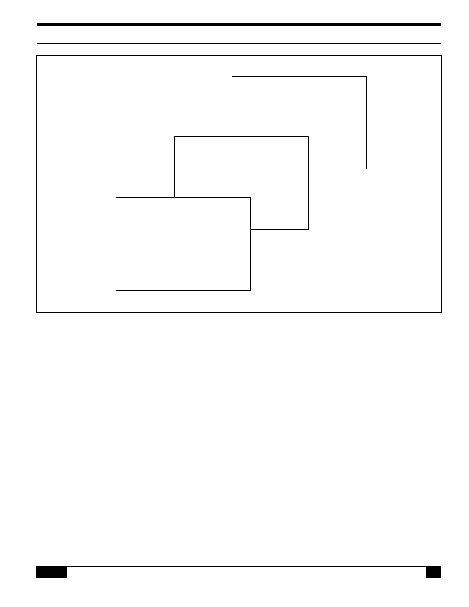
S-MOS Systems, Inc. · 2460 North First Street · San Jose, CA 95131 · Tel: (408) 922-0200 · Fax: (408) 922-0238
268-0.4
131
9.1.5
9.0 Application Notes
5DBFH
1F40H
2nd graphics layer
(8000 bytes)
3E7FH
0000H
1st graphics layer
(8000 bytes)
1F3FH
3E80H
3rd graphics layer
(8000 bytes)
Figure 83. Three-layer graphics
· Register setup procedure
SYSTEM SET
TC/R calculation
C =
40H
P1 =
30H
f
OSC
= 6 MHz
P2 =
87H
f
FR
= 70 Hz
P3 =
07H
P4 =
27H
(1/6)
×
9
×
[TC/R]
×
200 = 1/70
P5 =
2FH
[TC/R] = 48, so TC/R = 2FH
P6 =
C7H
P7 =
28H
P8 =
00H
SCROLL
C =
44H
P1 =
00H
P2 =
00H
P3 =
C8H
P4 =
40H
P5 =
1FH
P6 =
C8H
P7 =
80H
P8 =
3EH
P9 =
XH
P10 =
XH
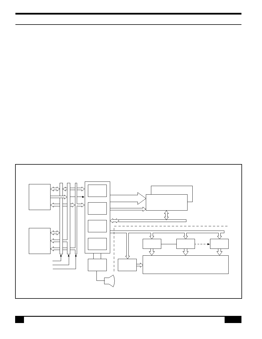
S-MOS Systems, Inc. · 2460 North First Street · San Jose, CA 95131 · Tel: (408) 922-0200 · Fax: (408) 922-0238
132
268-0.4
9.0 Application Notes
9.1.5 9.2
CSR FORM
C =
5DH
P1 =
07H
P2 =
87H
HDOT SCR
C =
5AH
P1 =
00H
OVLAY
C =
5BH
P1 =
1CH
DISP ON/OFF
C =
59H
P1 =
16H
X = Don't care
9.2 System Overview
Figure 84 shows the SED1330F/1335F/1336F in a
typical system. The microprocessor issues instruc-
tions to the 1330F/SED1335F/1336F, and the
SED1330F/1335F/1336F drives the LCD panel and
may have up to 64Kbytes of display memory.
Since all of the LCD control circuits are integrated
onto the SED1330F/1335F/1336F, few external com-
ponents are required to construct a complete me-
dium-resolution liquid crystal display.
External character
generator memory
Data bus
Address bus
Control bus
Character
generator
Display
address
control
Driver
control
TV
control*
Composite
signal
Y driver
Main
memory
Micro-
processor
Display memory
X driver
X driver
X driver
LCD panel
SED1335F/1336F
Display memory
address bus
Display memory
data bus
LCD unit
Driver bus
* SED1336F only
TV
Figure 84. System block diagram
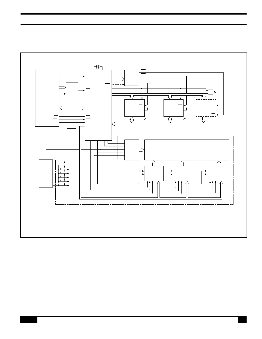
S-MOS Systems, Inc. · 2460 North First Street · San Jose, CA 95131 · Tel: (408) 922-0200 · Fax: (408) 922-0238
268-0.4
133
9.3 9.3.1
9.0 Application Notes
9.3 System Interconnection
9.3.1 SED1330F/1335F
Figure 85. System interconnection diagram
CS7
CS6
to
CS0
SED1630F
LAT
DI
INH
FR
YSCL
V
1
V
2
V
3
V
4
V
5
V
REG
P
OFF
A0
A1
to
A7
IORQ
D0
to
D7
RD
WR
RES
Decoder
A0
CS
D0
to
D7
RD
WR
RES
XD0
to
XD3
SED1335F
OSC1 OSC2
VA13
to
VA15
VCE
VR/W
VA0
to
VA12
VD0
to
VD7
XECL
XSCL
LP
WF
YDIS
YD
YSCL
A0 to A12
SRM2064
(RAM1)
D0 to D7
WE
CS1
CS2
OE
A0 to A12
SRM2064
(RAM2)
D0 to D7
WE
CS1
CS2
OE
A0 to A11
2732
(CGROM)
D0 to D7
VA12
Y7
Y6
to
Y0
A
B
C
10MHz crystal
OE
CE
LCD UNIT
SED1600F
HC138
RESET
LCD
LP
XSCL
ECL
DO
to
D3
E0
FR
E1
LP
XSCL
ECL
DO
to
D3
FR
EI
LP
XSCL
ECL
DO
to
D3
E0
FR
EI
LP
XSCL
ECL
DO
to
D3
E0
FR
EI
Power
supply
converter
Micro-
processor
SED1600F
SED1600F
SED1600F
Notes:
1. The recommended common drivers are the SED1743, SED1635.
2. The recommended segment drivers are the SED1742 and SED1606.
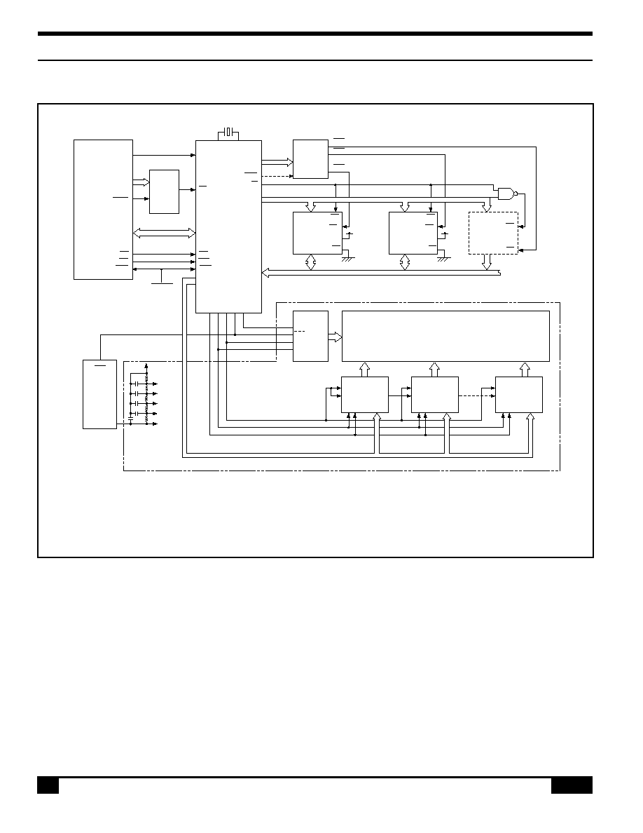
S-MOS Systems, Inc. · 2460 North First Street · San Jose, CA 95131 · Tel: (408) 922-0200 · Fax: (408) 922-0238
134
268-0.4
9.0 Application Notes
9.3.2
9.3.2 SED1336F
Figure 86. System interconnection diagram
The SED1330F/1335F/1336F's layered screens and
flexible scrolling facilities support a range of display
functions and reduces the load on the controlling
microprocessor when displaying underlining, inverse
display, text overlaid on graphics or simple animation.
These facilities are supported by the SED1330F/
1335F/1336F's ability to divide display memory into
up to four different areas.
· Character code table
· Contains character codes for text display
· Each character requires 8 bits
· Table mapping can be changed by using
the scroll start function
CS7
CS6
to
CS0
SED1630F
DI
INH
FR
YSCL
V
1
V
2
V
3
V
4
V
5
V
REG
P
OFF
A0
A1
to
A7
IORQ
D0
to
D7
RD
WR
RES
Decoder
A0
CS
D0
to
D7
RD
WR
RES
XD0
to
XD3
SED1336F
OSC1 OSC2
VA13
to
VA15
VCE
VR/W
VA0
to
VA12
VD0
to
VD7
XSCL
LP
WF
YDIS
YD
A0 to A12
SRM2064
(RAM1)
D0 to D7
WE
CS1
CS2
OE
A0 to A12
SRM2064
(RAM2)
D0 to D7
WE
CS1
CS2
OE
A0 to A11
2732
(CGROM)
D0 to D7
VA12
Y7
Y6
to
Y0
A
B
C
10MHz crystal
OE
CE
LCD UNIT
SED1600F
HC138
RESET
LCD
LP
XSCL
ECL
DO
to
D3
E0
FR
E1
LP
XSCL
DO
to
D3
FR
EI
LP
XSCL
DO
to
D3
E0
FR
EI
LP
XSCL
DO
to
D3
E0
FR
EI
Power
supply
converter
Micro-
processor
SED1600F
SED1600F
SED1600F
Notes:
1. The recommended common drivers are the SED1743, SED1635.
2. The recommended segment drivers are the SED1742 and SED1606.

S-MOS Systems, Inc. · 2460 North First Street · San Jose, CA 95131 · Tel: (408) 922-0200 · Fax: (408) 922-0238
268-0.4
135
9.3.2 9.4
9.0 Application Notes
· Graphics data table
· Contains graphics bitmaps
· Word length is 8 bits
· Table mapping can be changed
· CG RAM table
· Character generator memory can be
modified by the external microprocessor
· Character sizes up to 8
×
16 pixels (16
bytes per character)
· Maximum of 64 characters
· Table mapping can be changed
· CG ROM table
· Used when the internal character genera-
tor is not adequate
· Can be used in conjunction with the inter-
nal character generator and external char-
acter generator RAM
· Character sizes up to 8
×
16-pixels (16
bytes per character)
· Maximum of 256 characters
· Fixed mapping at F000H to FFFFH
9.4 Smooth Horizontal Scrolling
Figure 87 illustrates smooth display scrolling to the
left. When scrolling left, the screen is effectively
moving to the right, over the larger virtual screen.
Instead of changing the display start address SAD
and shifting the display by eight pixels, smooth scroll-
ing is achieved by repeatedly changing the pixel-shift
parameter of the HDOT SCR command. When the
display has been scrolled seven pixels, the HDOT
SCR pixel-shift parameter is reset to zero and SAD
incremented by one. Repeating this operation at a
suitable rate gives the appearance of smooth scroll-
ing.
To scroll the display to the right, the reverse proce-
dure is followed.
When the edge of the virtual screen is reached, the
microprocessor must take appropriate steps so that
the display is not corrupted. The scroll must be stopped
or the display modified.
Note that the HDOT SCR command cannot be used
to scroll individual layers.
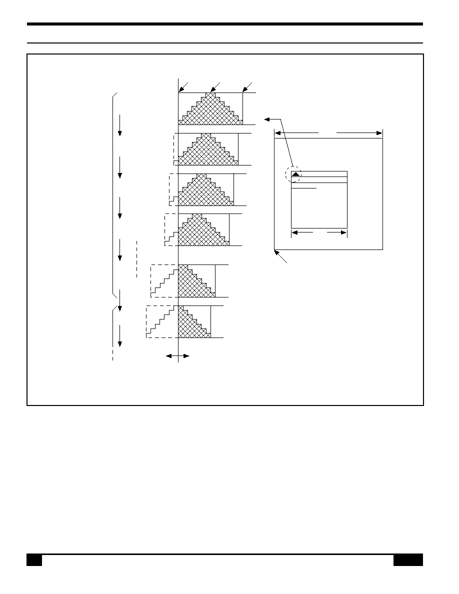
S-MOS Systems, Inc. · 2460 North First Street · San Jose, CA 95131 · Tel: (408) 922-0200 · Fax: (408) 922-0238
136
268-0.4
9.0 Application Notes
9.4
Display
AP
AP
P1 = 00H
P1 = 01H
P1 = 02H
P1 = 03H
P1 = 07H
P1 = 00H
HDOT SCR
parameter
SAD
SAD + 1
SAD + 2
SAD = SAD + 1
SAD = SAD
Not visible
Visible
C/R
Virtual screen
Magnified
Note: The response time of LCD panels changes considerably at low temperatures. Smooth scrolling under these conditions may
make the display difficult to read.
Figure 87. HDOT SCR example
S-MOS Systems, Inc. · 2460 North First Street · San Jose, CA 95131 · Tel: (408) 922-0200 · Fax: (408) 922-0238
268-0.4
137
9.5 9.5.2.1
9.0 Application Notes
9.5 Layered Display Attributes
SED1330F/1335F/1336F incorporates a number of
functions for enhanced displays using monochrome
LCD panels. It allows the display of inverse charac-
ters, half-intensity menu pads and flashing of selected
screen areas. These functions are controlled by the
OVLAY and DISP ON/OFF commands.
A number of means can be used to achieve these
effects, depending on the display configuration. These
are listed below. Note, however, that not all of these
can be used in the one layer at the same time.
Error
Attribute
Reverse
Half-tone
Local flashing
Ruled line
MX1
0
1
0
1
0
0
0
0
1
MX0
1
1
0
1
0
1
0
1
1
Combined layer display
IV
ME
BL
RL
LINE
LINE
Yes, No
EPSON
Error
1st layer display
IV
ME
BL
RL
LINE
LINE
Yes, No
EPSON
2ndt layer display
Figure 88. Layer synthesis
9.5.1 Inverse Display
The first layer is text, the second layer is graphics.
1. CSRW, CSDIR, MWRITE
Write 1s into the graphics screen at the area to
be inverted.
2. OVLAY: MX0 = 1, MX1 = 0
Set the combination of the two layers to
Exclusive-OR.
3. DISP ON/OFF: FP0 = FP1 = 1, FP1 = FP3 =
0.
Turn on layers 1 and 2.
9.5.2 Half-tone Display
The FP parameter can be used to generate half-
intensity display by flashing the display at 17 Hz. Note
that this mode of operation may cause flicker prob-
lems with certain LCD panels.
9.5.2.1 Menu Pad Display
Turn flashing off for the first layer, on at 17 Hz for the
second layer, and combine the screens using the OR
function.
1. OVLAY: P1 = 00H
2. DISP ON/OFF: P1 = 34H
S-MOS Systems, Inc. · 2460 North First Street · San Jose, CA 95131 · Tel: (408) 922-0200 · Fax: (408) 922-0238
138
268-0.4
9.0 Application Notes
9.5.2.1 9.5.3.2
Figure 89. Half-tone character and graphics
9.5.2.2 Graph Display
To present two overlaid graphs on the screen, config-
ure the display as for the menu bar display and put one
graph on each screen layer. The difference in contrast
between the half- and full-intensity displays will make
it easy to distinguish between the two graphs and help
create an attractive display.
1. OVLAY: P1 = 00H
2. DISP ON/OFF: P1 = 34H
9.5.3 Flashing Areas
9.5.3.1 Small Area
To flash selected characters, the MPU can alternately
write the characters as character codes and blank
characters at intervals of 0.5 to 1.0 seconds.
9.5.3.2 Large Area
Divide both layer 1 and layer 2 into two screen blocks
each, layer 2 being divided into the area to be flashed
and the remainder of the screen. Flash the layer 2
screen block at 2 Hz for the area to be flashed and
combine the layers using the OR function.
Figure 90. Localized flashing
AB
SAD1
1st layer
SAD2
2nd layer
AB
Combined layer display
+
Half-tone
ABC
XYZ
ABC
XYZ
S-MOS Systems, Inc. · 2460 North First Street · San Jose, CA 95131 · Tel: (408) 922-0200 · Fax: (408) 922-0238
268-0.4
139
9.6 9.6.2
9.0 Application Notes
9.6 16
×
16-dot Graphic Display
9.6.1 Command Usage
This example shows how to display 16
×
16-pixel
characters. The command sequence is as follows:
CSRW
Set the cursor address.
CSRDIR Set the cursor auto-increment di-
rection.
MWRITE Write to the display memory.
9.6.2 Kanji Character Display
The program for writing large characters operates as
follows:
1. The microprocessor reads the character data
from its ROM.
2. The microprocessor sets the display address
and writes to the VRAM. The flowchart is
shown in Figure 91.
(1)
(3)
(5)
(7)
(9)
(11)
(13)
(15)
(17)
(19)
(21)
(23)
(25)
(27)
(29)
(31)
(2)
(4)
(6)
(8)
(10)
(12)
(14)
(16)
(18)
(20)
(22)
(24)
(26)
(28)
(30)
(32)
O
8
O
7
O
6
O
5
O
4
O
3
O
2
O
1
O
8
O
7
O
6
O
5
O
4
O
3
O
2
O
1
(6)
(4)
(2)
(19)
(17)
(15)
(13)
(11)
(9)
(7)
(5)
(3)
(1)
0H
1H
2H
3H
4H
5H
6H
7H
8H
9H
AH
BH
CH
DH
EH
FH
Data held in the microprocessor memory
Scan address A1 to A4
1st column
2nd column
(n) shows the CG ROM data
readout order
(Kanji ROM pattern)
CG ROM output
A
0
= 0
A
0
= 1
(4)
(2)
(3)
(1)
Data written into the SED1330 display memory
2nd column
memory area
1st column
memory area
Figure 91. Graphics address indexing
S-MOS Systems, Inc. · 2460 North First Street · San Jose, CA 95131 · Tel: (408) 922-0200 · Fax: (408) 922-0238
140
268-0.4
9.0 Application Notes
9.6 9.6.2
(1)
(3)
(5)
(7)
(9)
(11)
(13)
(15)
(17)
(19)
(21)
(23)
(25)
(27)
(29)
(31)
(2)
(4)
(6)
(8)
(10)
(12)
(14)
(16)
(18)
(20)
(22)
(24)
(26)
(28)
(30)
(32)
Direction of cursor movement
240 dots
320 dots
Figure 92. Graphics bit map
Figure 93. 16
×
16-dot display flowchart
Start
Enable cursor downwards movement
Set column 1 cursor address
Write data
Set column 2 cursor address
Write data
End
Using an external character generator ROM, and 8
×
16-pixel font can be used, allowing a 16
×
16-pixel
character to be displayed in two segments. The exter-
nal CG ROM EPROM data format is described in
Section 5.1. This will allow the display of up to 128, 16
×
16-pixel characters. If CG RAM is also used, 96 fixed
characters and 32 bank-switchable characters can
also be supported.

S-MOS Systems, Inc. · 2460 North First Street · San Jose, CA 95131 · Tel: (408) 922-0200 · Fax: (408) 922-0238
268-0.4
141
10.0
Internal Character
Generator Font

S-MOS Systems, Inc. · 2460 North First Street · San Jose, CA 95131 · Tel: (408) 922-0200 · Fax: (408) 922-0238
142
268-0.4
THIS PAGE INTENTIONALLY BLANK
S-MOS Systems, Inc. · 2460 North First Street · San Jose, CA 95131 · Tel: (408) 922-0200 · Fax: (408) 922-0238
268-0.4
143
10.0
10.0 Internal Character Generator Font
10.0 Internal Character Generator Font
0
1
2
3
4
5
6
7
8
9
A
B
C
D
E
F
2
3
4
5
6
7
A
B
C
D
1
Character code bits 0 to 3
Character code bits 4 to 7
Figure 94. On-chip character set
Note: The shaded positions indicate characters that have the whole 6
×
8 bitmap blackened.

S-MOS Systems, Inc. · 2460 North First Street · San Jose, CA 95131 · Tel: (408) 922-0200 · Fax: (408) 922-0238
144
268-0.4
THIS PAGE INTENTIONALLY BLANK

S-MOS Systems, Inc. · 2460 North First Street · San Jose, CA 95131 · Tel: (408) 922-0200 · Fax: (408) 922-0238
268-0.4
145
11.0
Glossary of Terms

S-MOS Systems, Inc. · 2460 North First Street · San Jose, CA 95131 · Tel: (408) 922-0200 · Fax: (408) 922-0238
146
268-0.4
THIS PAGE INTENTIONALLY BLANK

S-MOS Systems, Inc. · 2460 North First Street · San Jose, CA 95131 · Tel: (408) 922-0200 · Fax: (408) 922-0238
268-0.4
147
11.0
11.0 Glossary of Terms
11.0 Glossary of Terms
A
Address
AP
Address pitch parameter
C
Character display mode
CD
Cursor direction of movement parameter
CG
Character generator
CGRAM ADR
Character generator memory address
CM
Cursor display shape parameter
C/R
Characters per row parameter
CRX
Horizontal cursor size parameter
CRY
Vertical cursor size parameter
CSR DIR
Cursor direction of movement instruction
CSR FORM
Cursor size, position and type instruction
CSRR
Read cursor address register instruction
CSRW
Write cursor address register instruction
DM
Display mode parameter
FC
Flashing cursor parameter
f
FR
Frame frequency
f
OSC
Oscillator frequency
FP
Screen flashing parameter
FX
Horizontal character size parameter
FY
Vertical character size parameter
G
Graphics display mode
GLC
Graphic line control unit
HDOT SCR
Horizontal scrolling by pixels instruction
IV
Screen origin compensation for inverse display
L/F
Lines per frame instruction
S-MOS Systems, Inc. · 2460 North First Street · San Jose, CA 95131 · Tel: (408) 922-0200 · Fax: (408) 922-0238
148
268-0.4
MREAD
Display memory read instruction
MWRITE
Display memory write instruction
MX
Screen composition mode
OV
Graphics layer select parameter
OVLAY
Screen layer mode instruction
P
Parameter
R
Row
RAM
Random access memory
ROM
Read only memory
SAD
Display scrolling start address parameter
SL
Display scrolling length parameter
TC/R
Length, including horizontal blanking, of one screen line
VRAM
Display memory
WF
Display drive waveform parameter
W/S
Windows per screen parameter
11.0 Glossary of Terms
11.0
S-MOS assumes no responsibility or liability for (1) any errors or inaccuracies contained in the
information herein and (2) the use of the information or a portion thereof in any application,
including any claim for (a) copyright or patent infringement or (b) direct, indirect, special or
consequential damages. There are no warranties extended or granted by this document. The
information herein is subject to change without notice from S-MOS.
September 1995
© Copyright 1995 S-MOS Systems, Inc.
Printed in U.S.A.
268-0.4
Document Outline
- Graphics Main Menu
- SED1330 Data Sheet
- SED1335 Data Sheet
- SED1336 Data Sheet