
Parameter
Input Voltage
DC Output Current
Ambient Operating Temperature
Symbol
V
IN
I
O
T
op
s
Features
∑ Compact surface-mount package (SOT-89-3)
∑ Output current: 250 mA
∑ Low dropout voltage: V
DIF
0.5 V (at I
O
= 250 mA)
∑ 4 types of output voltages (1.8 V, 2.5 V, 3.3 V, 5.0 V) available
∑ Built-in dropping type overcurrent, thermal protection circuits
s
Applications
∑ Auxiliary power supply for PC
∑ Battery-driven electronic equipment
s
Absolute Maximum Ratings
SI-3000LUS Series
q
SI-3000LUS Series
Ratings
min.
max.
*2
V
O
+2
*1
0
250
≠20
85
Unit
V
mA
W
∞
C
∞
C
∞
C/W
Ratings
18
250
0.75
≠40 to +135
≠40 to +125
146
Symbol
V
IN
I
O
P
D
*1
T
j
*2
T
op
*2
j-a
*1
Parameter
DC Input Voltage
DC Output Current
Power Dissipation
Junction Temperature
Storage Temperature
Thermal Resistance (Junction to Ambient Air)
(T
a
=25
∞
C)
*1: When mounted on glass-epoxy board 40
◊
40 mm (copper laminate area 2%)
*2: Thermal protection circuits may operate if the junction temperature exceeds 135
∞
C
s
Recommended Operating Conditions
*1: V
IN
(max) and I
O
(max) are restricted by the relationship P
D
= (V
IN
- V
O
)
◊
I
O
.
Calculate these values referring to the reference data.
*2: Refer to the dropout voltage section.
Unit
V
mA
∞
C
Surface-Mount, Low Current Consumption, Low Dropout Voltage Dropper Type

Parameter
Output Voltage
Dropout Voltage
Line Regulation
Load Regulation
Temperature Coeffi-
cient of Output Voltage
Ripple Rejection
Quiescent Circuit
Current
Overcurrent Protection
Starting Current
*1
Symbol
V
O
Conditions
V
DIF
Conditions
Conditions
V
LINE
Conditions
V
LOAD
Conditions
V
O
/
T
a
Conditions
R
REJ
Conditions
I
q
Conditions
I
S1
Conditions
s
Electrical Characteristics
*1: Is
1
is specified as the 5% drop point of output voltage V
O
on the condition that V
IN
=3.3 V (5 V for SI-3033LUS, 6 V for SI-3050LUS),
and I
O
=10 mA.
s
External Dimensions
Pin Arrangement
q
V
IN
w
GND
e
V
OUT
Plastic Mold Package Type
Flammability: UL94V-0
Weight: Approx. 0.05g
q
SI-3000LUS Series
(Unit : mm)
(T
a
=25
∞
C, V
C
=2V unless otherwise specified)
Unit
V
V
mV
mV
mV/
∞
C
dB
µ
A
mA
Ratings
SI-3018LUS
SI-3025LUS
SI-3033LUS
SI-3050LUS
min.
typ.
max.
min.
typ.
max.
min.
typ.
max.
min.
typ.
max.
1.764
1.800
1.836
2.450
2.500
2.550
3.234
3.300
3.366
4.900
5.000
5.100
V
IN
=3.3V, I
O
=10mA
V
IN
=3.3V, I
O
=10mA
V
IN
=5V, I
O
=10mA
V
IN
=6V, I
O
=10mA
0.3
0.3
0.3
0.3
I
O
=100mA
0.5
0.5
0.5
0.5
I
O
=250mA
10
10
10
10
V
IN
=3.3 to 5V, I
O
=10mA
V
IN
=3.3 to 5V, I
O
=10mA
V
IN
=4.5 to 8V, I
O
=10mA
V
IN
=6 to 10V, I
O
=10mA
40
40
40
40
V
IN
=3.3V, I
O
=0 to 250mA
V
IN
=3.3V, I
O
=0 to 250mA
V
IN
=5V, I
O
=0 to 250mA
V
IN
=6V, I
O
=0 to 250mA
±
0.25
±
0.25
±
0.3
±
0.3
T
j
=0 to 100
∞
C
55
55
55
55
V
IN
=3.3V, f=100 to 120H
Z
V
IN
=3.3V, f=100 to 120H
Z
V
IN
=5V, f=100 to 120H
Z
V
IN
=6V, f=100 to 120H
Z
250
250
250
250
V
IN
=3.3V, I
O
=0mA
V
IN
=3.3V, I
O
=0mA
V
IN
=5V, I
O
=0mA
V
IN
=6V, I
O
=0mA
260
260
260
260
V
IN
=3.3V
V
IN
=3.3V
V
IN
=5V
V
IN
=6V
4.5
0.49max.
0.49max.
0.54
max.
1.5
1.5
0.16
(1.7)
0.4
1.6
1
2
3
(R0.3)
(R0.15)
2.5
(0.4)
4.25max.
1.5
(0.1)
0.25
0.8min.
45
∞
(5
∞
)
(8
∞
)
(8
∞
)
(5
∞
)
( 1.0)
(Under
development)
(Under
development)
(Under
development)
q
SI-3000LUS Series
s
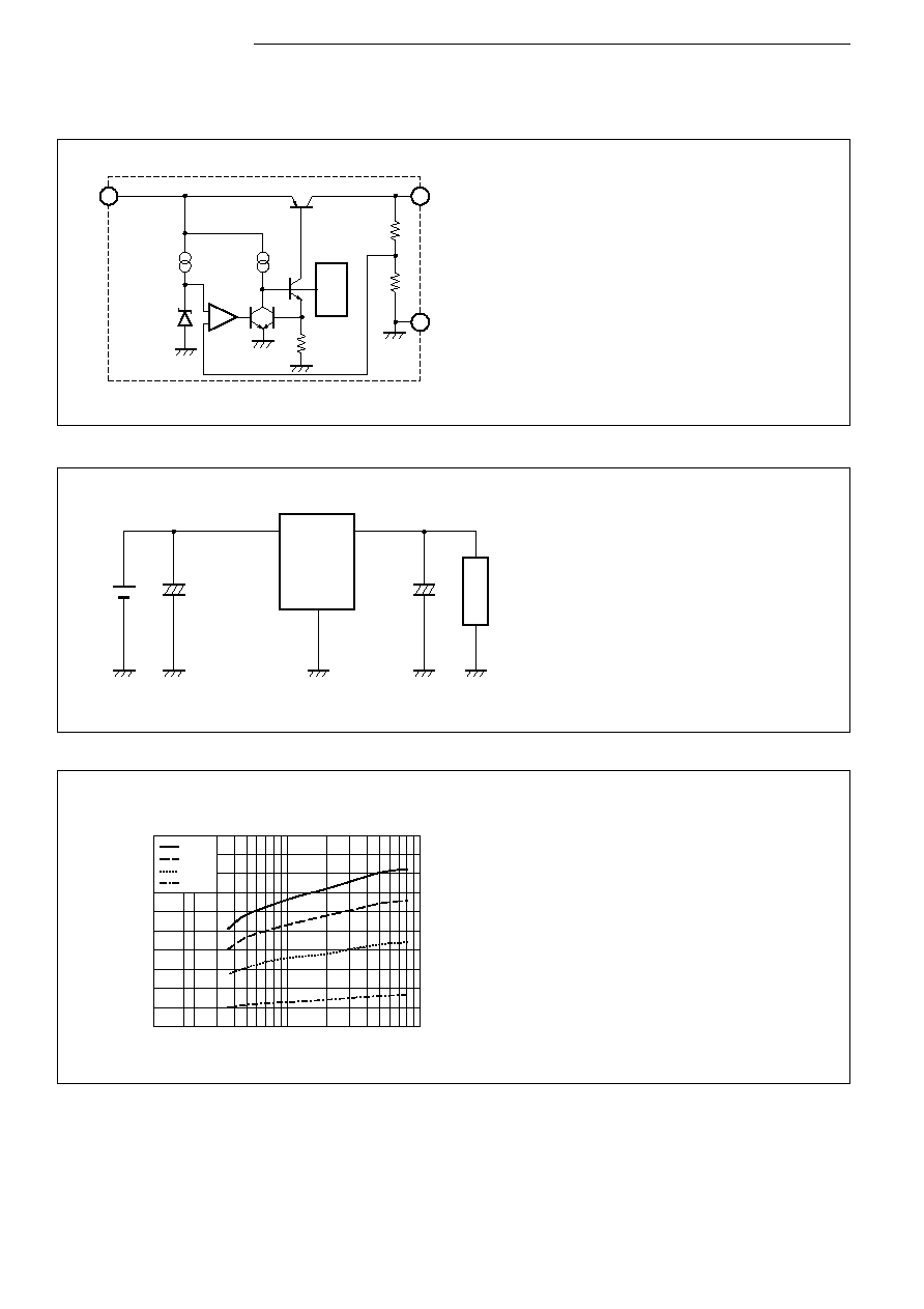
Block Diagram
s
Standard External Circuit
s
Reference Data
C
O
: Output capacitor (10
µ
F or larger)
The SI-3000LUS series can be operated on the circuit
even if a low ESR ceramic capacitor is used as the
output capacitor.
C
IN
:Input capacitor (0.1 to 10
µ
F)
This capacitor is required in the case of an inductive
input line or long wiring.
∑ A monolithic IC is mounted. The inner frame stage is con-
nected to the GND pin (pin 2). Therefore, enlarging the
copper laminate area leading to the GND pin achieves a
heat radiation effect.
∑ How to calculate the junction temperature
Measure the temperature (T
C
) of the GND pin (pin 2) lead
section using a thermistor, etc. Substitute this value in the
following formula and calculate the junction temperature.
T
j
=P
D
◊
j≠c+Tc (
j≠c=5
∞
C/W)
REF
TSD
+
≠
V
IN
V
O
GND
1
3
2
1
3
2
+
V
IN
V
IN
V
O
C
IN
Load
C
O
GND
+
1
0.9
0.8
0.7
0.6
0.5
0.4
0.3
0.2
0.1
0
10
100
1000
Copper Laminate Area (mm
2
)
Power Dissipation P
D
(W)
Ta=25
∞
C
Ta=40
∞
C
Ta=60
∞
C
Ta=85
∞
C
Copper Laminate Area vs. Power Dissipation
T
j
=100
∞
C PWB size 40
◊
40

q
SI-3000LUS Series
s
Typical Characteristics of SI-3033LUS
(T
a
=25
∞
C)
I
O
vs. V
DIF
Characteristics
Output Voltage Characteristics
Line Regulation
Load Regulation
Overcurrent Protection Characteristics
0
50
100
150
200
250
300
0.6
0.5
0.4
0.3
0.2
0.1
Output Current I
O
(mA)
Dropout Voltage V
DIF
(V)
0
2
4
6
8
10
5
4
3
2
1
Input Voltage V
IN
(V)
Output Voltage V
O
(V)
l
O
=0mA
l
O
=250mA
0
4
6
8
10
3.34
3.32
3.30
3.28
3.26
3.24
3.22
Input Voltage V
IN
(V)
Output Voltage V
O
(V)
l
O
=0mA
l
O
=250mA
8V
6V
5V
V
IN
=3.8V
0
50
100
150
200
250
300
3.34
3.32
3.30
3.28
3.26
3.24
3.22
Output Current I
O
(mA)
Dropout Voltage V
DIF
(V)
5
4
3
2
1
0
0
100
200
300
400
Output Current I
O
(mA)
Output Voltage V
O
(V)
V
IN
=3.8V
5V
8, 10V