 | –≠–ª–µ–∫—Ç—Ä–æ–Ω–Ω—ã–π –∫–æ–º–ø–æ–Ω–µ–Ω—Ç: Si4123-BT | –°–∫–∞—á–∞—Ç—å:  PDF PDF  ZIP ZIP |
Rev. 1.1 3/01
Copyright © 2001 by Silicon Laboratories
Si4133-DS11
This information applies to a product under development. Its characteristics and specifications are subject to change without notice.
Si4133
Si4123/22/13/12
D
U A L
-B
A N D
RF S
Y N T H E S I Z E R
W
I T H
I
N T E G R A T E D
VCO
S
F
O R
W
I R E L E S S
C
O M M U N I C A T I O N S
Features
Applications
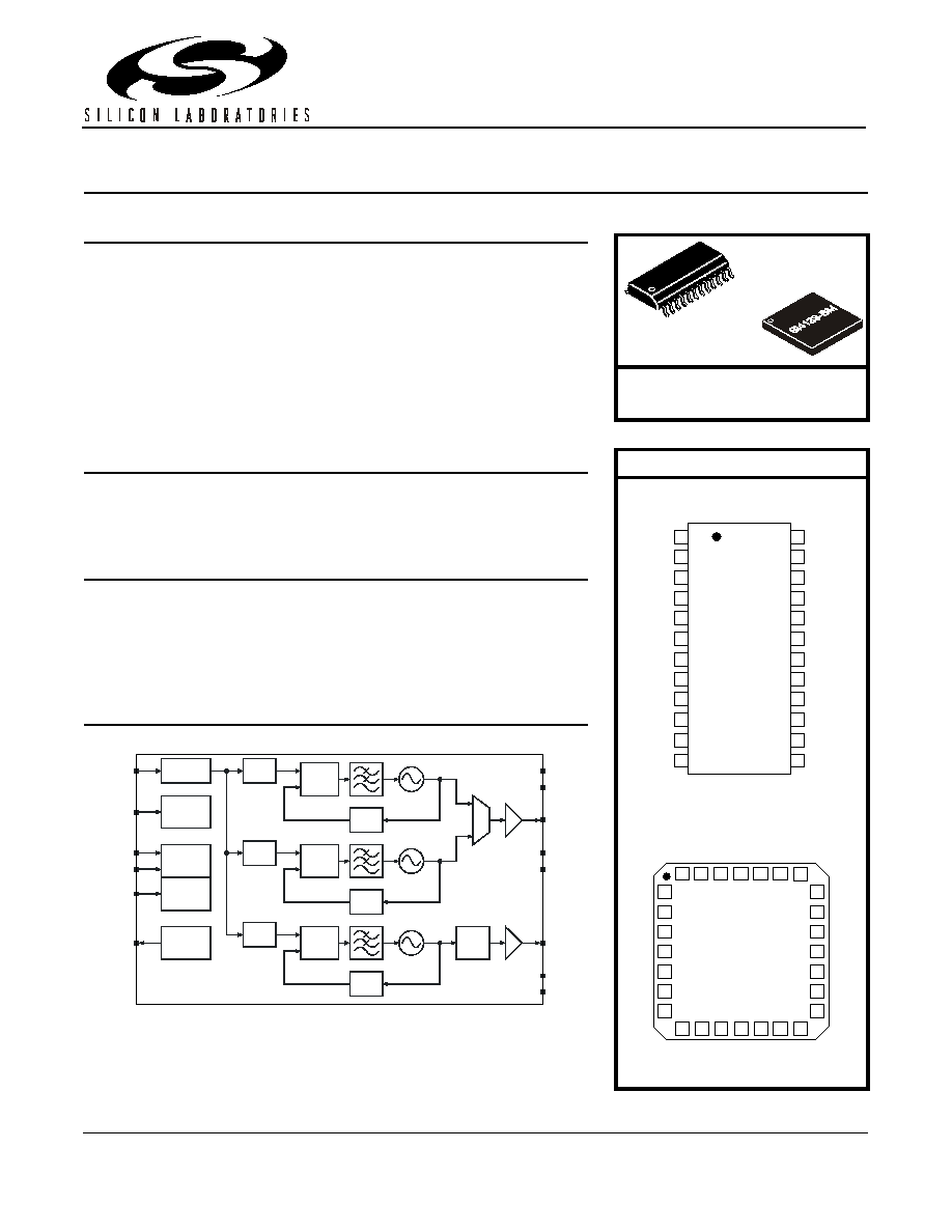
Description
The Si4133 is a monolithic integrated circuit that performs both IF and dual-
band RF synthesis for wireless communications applications. The Si4133
includes three VCOs, loop filters, reference and VCO dividers, and phase
detectors. Divider and power-down settings are programmable through a
three-wire serial interface.
Functional Block Diagram
!
Dual-Band RF Synthesizers
"
RF1: 900 MHz to 1.8 GHz
"
RF2: 750 MHz to 1.5 GHz
!
IF Synthesizer
"
IF: 62.5 MHz to 1000 MHz
!
Integrated VCOs, Loop Filters,
Varactors, and Resonators
!
Minimal (2) External
Components Required
!
Low Phase Noise
!
Programmable Power Down Modes
!
1 µA Standby Current
!
18 mA Typical Supply Current
!
2.7 V to 3.6 V Operation
!
Packages: 24-Pin TSSOP, 28-Lead
MLP
!
Dual-Band Communications
!
Digital Cellular Telephones
GSM, DCS1800, PCS1900
!
Digital Cordless Phones
!
Analog Cordless Phones
!
Wireless LAN and WAN
IFOU T
IFLA
IFLB
R FOUT
XIN
PW D N B
SD ATA
SC LK
SENB
IF
R F2
R F1
Pow er
D ow n
C ontrol
R eference
Am plifier
Serial
Interface
AU XOU T
IFD IV
˜
R
˜
R
˜
R
˜
N
˜
N
˜
N
Phase
D etector
22-bit
D ata
R egister
Test
Mux
R FLC
R FLD
R FLA
R FLB
Phase
D etector
Phase
D etector
Patents pending
Ordering Information:
See page 31.
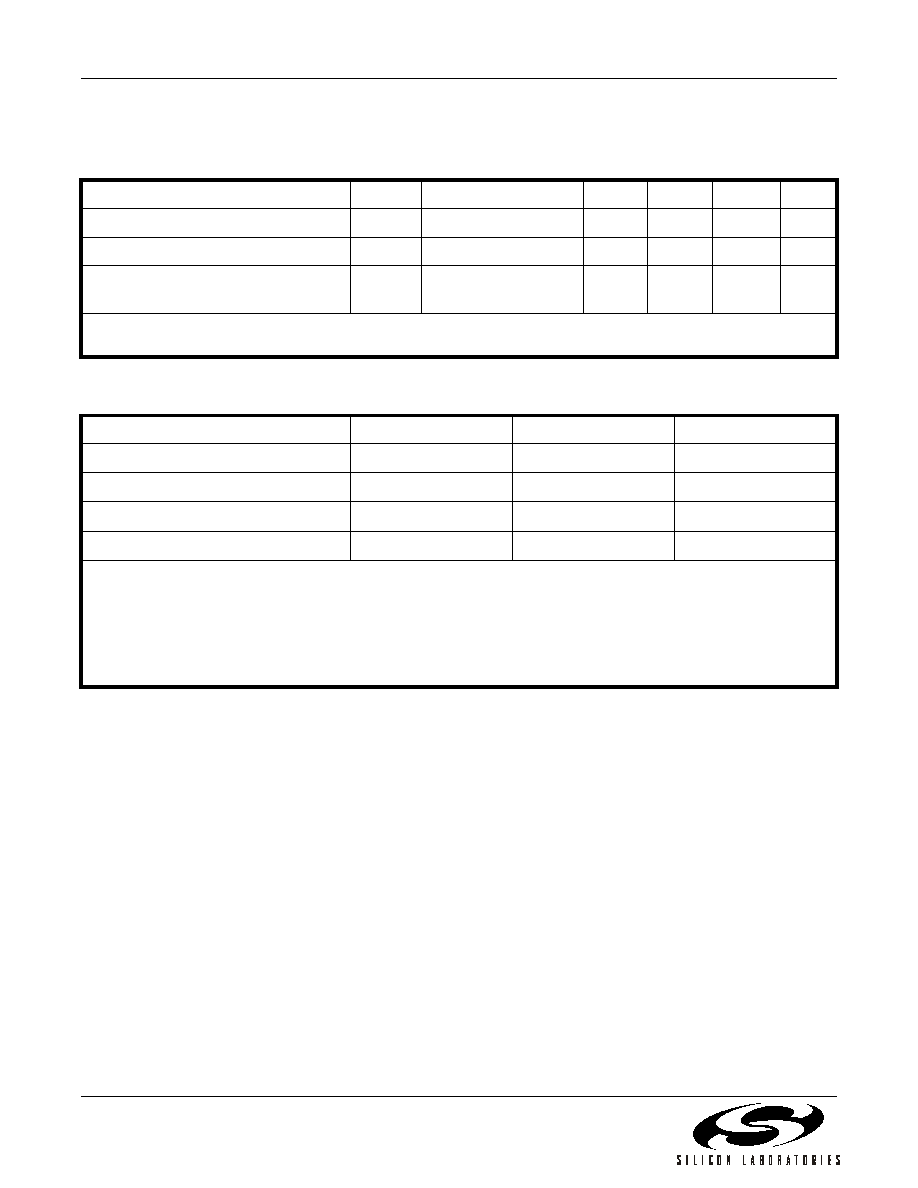
Pin Assignments
Si4133-BT
Si4133-BM
Si4133-BT
Si4133-BT
1
24
2
23
3
22
4
21
5
20
6
19
7
18
8
17
9
16
10
15
11
14
12
13
SCLK
SDA TA
GNDR
RFLD
RFLC
RFLB
GNDR
RFLA
GNDR
GNDR
RFOUT
V DDR
SENB
V DDI
IFOUT
GNDI
IFLB
IFLA
GNDD
V DDD
GNDD
XIN
PWDNB
A UXOUT
SC
L
K
SD
A
T
A
GN
D
R
RFLD
RFLC
RFLB
GNDR
RFLA
RF
O
U
T
VD
D
R
S
E
N
B
VD
D
I
IF
O
U
T
GNDI
IFLB
IFLA
GN
D
D
V DDD
GNDD
XIN
PW
D
N
B
AU
X
O
U
T
21
20
19
18
17
16
15
8
9
10
11
12
13
14
28
27
26
25
24
23
22
1
2
3
4
5
6
7
GN
D
R
GNDR
GNDR
GNDD
GN
D
I
GN
D
R

Si4133
2
Rev. 1.1

Si4133
Rev. 1.1
3
T
A B L E
O F
C
O N T E N T S
Section
Page
Electrical Specifications . . . . . . . . . . . . . . . . . . . . . . . . . . . . . . . . . . . . . . . . . . . . . . . . . 4
Functional Description . . . . . . . . . . . . . . . . . . . . . . . . . . . . . . . . . . . . . . . . . . . . . . . . . . 16
Serial Interface . . . . . . . . . . . . . . . . . . . . . . . . . . . . . . . . . . . . . . . . . . . . . . . . . . . . . . 16
Setting the VCO Center Frequencies . . . . . . . . . . . . . . . . . . . . . . . . . . . . . . . . . . . . . 16
Extended Frequency Operation . . . . . . . . . . . . . . . . . . . . . . . . . . . . . . . . . . . . . . . . . 17
Self-Tuning Algorithm . . . . . . . . . . . . . . . . . . . . . . . . . . . . . . . . . . . . . . . . . . . . . . . . . 17
Output Frequencies . . . . . . . . . . . . . . . . . . . . . . . . . . . . . . . . . . . . . . . . . . . . . . . . . . 18
PLL Loop Dynamics . . . . . . . . . . . . . . . . . . . . . . . . . . . . . . . . . . . . . . . . . . . . . . . . . . 18
RF and IF Outputs . . . . . . . . . . . . . . . . . . . . . . . . . . . . . . . . . . . . . . . . . . . . . . . . . . . 19
Reference Frequency Amplifier . . . . . . . . . . . . . . . . . . . . . . . . . . . . . . . . . . . . . . . . . 19
Power Down Modes . . . . . . . . . . . . . . . . . . . . . . . . . . . . . . . . . . . . . . . . . . . . . . . . . . 19
Auxiliary Output (AUXOUT) . . . . . . . . . . . . . . . . . . . . . . . . . . . . . . . . . . . . . . . . . . . . 20
Control Registers . . . . . . . . . . . . . . . . . . . . . . . . . . . . . . . . . . . . . . . . . . . . . . . . . . . . . . . 21
Pin Descriptions: Si4133-BT . . . . . . . . . . . . . . . . . . . . . . . . . . . . . . . . . . . . . . . . . . . . . . 27
Pin Descriptions: Si4133-BM . . . . . . . . . . . . . . . . . . . . . . . . . . . . . . . . . . . . . . . . . . . . . . 29
Ordering Guide . . . . . . . . . . . . . . . . . . . . . . . . . . . . . . . . . . . . . . . . . . . . . . . . . . . . . . . . . 31
Si4133 Derivative Devices . . . . . . . . . . . . . . . . . . . . . . . . . . . . . . . . . . . . . . . . . . . . . . . . 31
Package Outline: Si4133-BT . . . . . . . . . . . . . . . . . . . . . . . . . . . . . . . . . . . . . . . . . . . . . . 32
Package Outline: Si4133-BM . . . . . . . . . . . . . . . . . . . . . . . . . . . . . . . . . . . . . . . . . . . . . . 33
Contact Information . . . . . . . . . . . . . . . . . . . . . . . . . . . . . . . . . . . . . . . . . . . . . . . . . . . . . 34
Si4133
4
Rev. 1.1
Electrical Specifications
Table 1. Recommended Operating Conditions
Parameter
Symbol
Test Condition
Min
Typ
Max
Unit
Ambient Temperature
T
A
≠40
25
85
∞C
Supply Voltage
V
DD
2.7
3.0
3.6
V
Supply Voltages Difference
V
(V
DDR
≠ V
DDD
),
(V
DDI
≠ V
DDD
)
≠0.3
--
0.3
V
Note: All minimum and maximum specifications are guaranteed and apply across the recommended operating conditions.
Typical values apply at nominal supply voltages and an operating temperature of 25∞C unless otherwise stated.
Table 2. Absolute Maximum Ratings
1,2
Parameter
Symbol
Value
Unit
DC Supply Voltage
V
DD
≠0.5 to 4.0
V
Input Current
3
I
IN
±10
mA
Input Voltage
3
V
IN
≠0.3 to V
DD
+0.3
V
Storage Temperature Range
T
STG
≠55 to 150
o
C
Notes:
1. Permanent device damage may occur if the above Absolute Maximum Ratings are exceeded. Functional operation
should be restricted to the conditions as specified in the operational sections of this data sheet. Exposure to absolute
maximum rating conditions for extended periods may affect device reliability.
2. This device is a high performance RF integrated circuit with an ESD rating of < 2 kV. Handling and assembly of
this device should only be done at ESD-protected workstations.
3. For signals SCLK, SDATA, SENB, PWDNB and XIN.
Si4133
Rev. 1.1
5
Table 3. DC Characteristics
(V
DD
= 2.7 to 3.6 V, T
A
= ≠40 to 85∞C)
Parameter
Symbol
Test Condition
Min
Typ
Max
Unit
Total Supply Current
1
RF1 and IF operating
--
18
27
mA
RF1 Mode Supply Current
1
--
10
16
mA
RF2 Mode Supply Current
1
--
9
16
mA
IF Mode Supply Current
1
--
8
13
mA
Standby Current
PWDNB = 0
--
1
--
µA
High Level Input Voltage
2
V
IH
0.7 V
DD
--
--
V
Low Level Input Voltage
2
V
IL
--
--
0.3 V
DD
V
High Level Input Current
2
I
IH
V
IH
=
3.6 V,
V
DD
= 3.6 V
≠10
--
10
µA
Low Level Input Current
2
I
IL
V
IL
=
0 V,
V
DD
=
3.6 V
≠10
--
10
µA
High Level Output Voltage
3
V
OH
I
OH
= ≠500 µA
V
DD
≠0.4
--
--
V
Low Level Output Voltage
3
V
OL
I
OH
= 500 µA
--
--
0.4
V
Notes:
1. RF1 = 1.6 GHz, RF2 = 1.1 GHz, IFOUT = 550 MHz, LPWR = 0
2. For signals SCLK, SDATA, SENB, and PWDNB.
3. For signal AUXOUT.