
Sunplus Technology reserves the right to change this documentation without prior notice. Information provided by Sunplus Technology is believed to be
accurate and reliable. However, Sunplus Technology makes no warranty for any errors which may appear in this document. Contact Sunplus Technology to
obtain the latest version of device specifications before placing your order. No responsibility is assumed by Sunplus Technology for any infringement of patent
or other rights of third parties which may result from its use. In addition, Sunplus products are not authorized for use as critical components in life support
devices/ systems or aviation devices/systems, where a malfunction or failure of the product may reasonably be expected to result in significant injury to the
user, without the express written approval of Sunplus.
FEB. 15, 2005
Version 1.7
S
S
P
P
L
L
C
C
7
7
8
8
2
2
A
A
1
1
6
6
C
C
O
O
M
M
/
/
8
8
0
0
S
S
E
E
G
G
C
C
o
o
n
n
t
t
r
r
o
o
l
l
l
l
e
e
r
r
/
/
D
D
r
r
i
i
v
v
e
e
r
r

SPLC782A
� Sunplus Technology Co., Ltd.
Proprietary & Confidential
2
FEB. 15, 2005
Version: 1.7
Table of Contents
PAGE
1.
GENERAL
DESCRIPTION .......................................................................................................................................................................... 4
2.
FEATURES.................................................................................................................................................................................................. 4
3.
BLOCK
DIAGRAM ...................................................................................................................................................................................... 4
4.
SIGNAL
DESCRIPTIONS............................................................................................................................................................................ 5
5.
FUNCTIONAL
DESCRIPTIONS.................................................................................................................................................................. 6
5.1.
O
SCILLATOR
.......................................................................................................................................................................................... 6
5.2.
C
ONTROL AND
D
ISPLAY
I
NSTRUCTIONS
................................................................................................................................................... 6
5.3.
I
NSTRUCTION
T
ABLE
............................................................................................................................................................................... 8
5.4.
8-B
IT
O
PERATION AND
16-D
IGIT
1-L
INE
D
ISPLAY
(U
SING
I
NTERNAL
R
ESET
).............................................................................................. 9
5.5.
4-B
IT
O
PERATION AND
16-D
IGIT
1-L
INE
D
ISPLAY
(U
SING
I
NTERNAL
R
ESET
)............................................................................................ 10
5.6.
8-B
IT
O
PERATION AND
16-D
IGIT
2-L
INE
D
ISPLAY
(U
SING
I
NTERNAL
R
ESET
)............................................................................................ 10
5.7.
R
ESET
F
UNCTION
.................................................................................................................................................................................11
5.8.
D
ISPLAY
D
ATA
RAM
(DD
RAM)............................................................................................................................................................ 13
5.9.
T
IMING
G
ENERATION
C
IRCUIT
............................................................................................................................................................... 13
5.10.
LCD
D
RIVER
C
IRCUIT
....................................................................................................................................................................... 13
5.11.
C
HARACTER
G
ENERATOR
ROM
(CG
ROM)....................................................................................................................................... 13
5.12.
C
HARACTER
G
ENERATOR
RAM
(CG
RAM)........................................................................................................................................ 13
5.13.
C
URSOR
/B
LINK
C
ONTROL
C
IRCUIT
.................................................................................................................................................... 17
5.14.
I
NTERFACING TO
MPU....................................................................................................................................................................... 18
5.15.
S
UPPLY
V
OLTAGE FOR
LCD
D
RIVE
..................................................................................................................................................... 20
5.16.
R
EGISTER
---
IR
(I
NSTRUCTION
R
EGISTER
)
AND
DR
(D
ATA
R
EGISTER
) ................................................................................................ 22
5.17.
B
USY
F
LAG
(BF) ............................................................................................................................................................................... 22
5.18.
A
DDRESS
C
OUNTER
(AC).................................................................................................................................................................. 22
5.19.
S
EGMENT
D
ATA
D
IRECTION
............................................................................................................................................................... 22
5.20.
C
OMMON
D
ATA
D
IRECTION
................................................................................................................................................................ 22
5.21.
I/O
P
ORT
C
ONFIGURATION
................................................................................................................................................................ 22
6.
ELECTRICAL
SPECIFICATIONS ............................................................................................................................................................. 24
6.1.
A
BSOLUTE
M
AXIMUM
R
ATINGS
............................................................................................................................................................. 24
6.2.
DC
C
HARACTERISTICS
(VDD
=
2.4V
TO
4.5V,
T
A
=
-20
TO
+75) .................................................................................................... 24
6.3.
DC
C
HARACTERISTICS
(VDD
=
4.5V
TO
5.5V,
T
A
=
-20
TO
+75) .................................................................................................... 25
6.4.
AC
C
HARACTERISTICS
(VDD
=
4.5V
TO
5.5V,
T
A
=
-20
TO
+75) .................................................................................................... 25
6.5.
AC
C
HARACTERISTICS
(VDD
=
2.4V
TO
4.5V,
T
A
=
-20
TO
+75) .................................................................................................... 26
6.6.
W
RITE
M
ODE
T
IMING
D
IAGRAM
(W
RITING
D
ATA FROM
MPU
TO
SPLC782A).......................................................................................... 27
6.7.
R
EAD
M
ODE
T
IMING
D
IAGRAM
(R
EADING
D
ATA FROM
SPLC782A
TO
MPU)........................................................................................... 27
6.8.
T
HE
F
OLLOWING
G
RAPS
S
HOW THE
R
ELATIONSHIP
B
ETWEEN
F
OSC
AND
T
EMPERATURE
......................................................................... 27
7.
APPLICATION
CIRCUITS ......................................................................................................................................................................... 28
7.1.
I
NTERFACE TO
MPU............................................................................................................................................................................. 28
7.2.
A
PPLICATIONS FOR
LCD ...................................................................................................................................................................... 29
8.
CHARACTER
GENERATOR
ROM ........................................................................................................................................................... 35
8.1.
SPLC782A
-
016 ................................................................................................................................................................................ 35
8.2.
SPLC782A
-
022 ................................................................................................................................................................................ 36
Sunplus Confidential
For PARTMINER Use Only

SPLC782A
� Sunplus Technology Co., Ltd.
Proprietary & Confidential
3
FEB. 15, 2005
Version: 1.7
9.
PACKAGE/PAD
LOCATIONS ................................................................................................................................................................... 37
9.1.
PAD
A
SSIGNMENT AND
L
OCATIONS
....................................................................................................................................................... 37
9.2.
O
RDERING
I
NFORMATION
..................................................................................................................................................................... 37
10.
DISCLAIMER............................................................................................................................................................................................. 38
11.
REVISION
HISTORY ................................................................................................................................................................................. 39
Sunplus Confidential
For PARTMINER Use Only
SPLC782A
� Sunplus Technology Co., Ltd.
Proprietary & Confidential
4
FEB. 15, 2005
Version: 1.7
16COM/80SEG CONTROLLER/DRIVER
1. GENERAL DESCRIPTION
The SPLC782A, a dot-matrix LCD controller and driver, is a
low-power CMOS integrated circuit. The SPLC782A is capable
of connecting with MPU for LCD application and easily to be used
for designing the low-cost products.
2. FEATURES
Character generator ROM: 10880 bits
Character font 5 x 8 dots: 192 characters
Character font 5 x 10 dots: 64 characters
4 type CGROM mode, Max. 256 characters can be used.
Character generator RAM: 512 bits
Character font 5 x 8 dots: 8 characters
Character font 5 x 10 dots: 4 characters
Provide connecting to 4-bit or 8-bit MPU
Direct driver for LCD: 16 COMs x 80 SEGs
80-channel Bi-Direction segment driver
16-channel Bi-direction common driver
Duty factor (selected by program):
1/8 duty: 1 line of 5 x 8 dots
1/11 duty: 1 line of 5 x 10 dots
1/16 duty: 2 lines of 5 x 8 dots / line
LCD type-A, type-B waveform can be selected.
Built-in power on automatic reset circuit
Built-in oscillator circuit (with internal resistor)
Built-in Bias resistor
Support external clock operation
Package form: Au bump chip
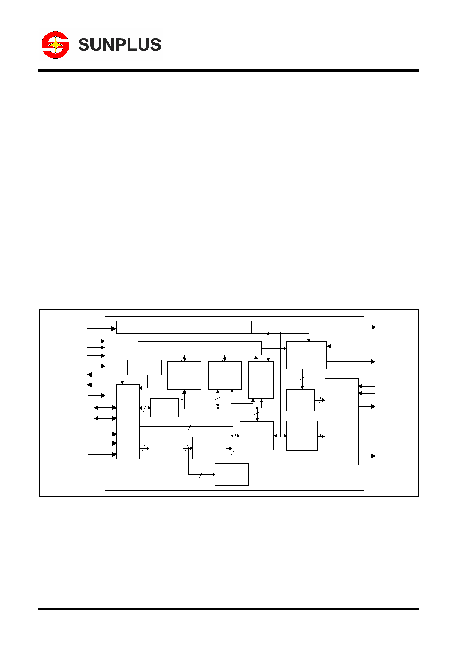
3. BLOCK DIAGRAM
Figure 3-1: Block Diagram
COM1-
COM16
SEG1-
SEG80
OSC1
I / O
Buffer
Timing Generation Circuit
80
Segments
x
16
Commons
LCD
Driver
Character
Generator
ROM
80-bit
Bi-Direction
Shift Register
Latch
Circuit
16-bit
Shift
Register
Parallel to Serial Data Conversion Circuit
Cursor
Blink
Control
Circuit
Character
Generator
RAM
Display
Data RAM
80 Bytes
Address
Counter
Instruction
Register
Data
Register
Busy Flag
Instruction
Decorder
5
5
8
8
8
8
7
7
7
8
7
8
80
16
80
CL2
E
RS
R / W
DB0-DB3
DB4-DB7
VSS
V2
V3
VPP
SHL
D
VDD
MOD1
MOD0
TYPE
DIRC
Sunplus Confidential
For PARTMINER Use Only
SPLC782A
� Sunplus Technology Co., Ltd.
Proprietary & Confidential
5
FEB. 15, 2005
Version: 1.7
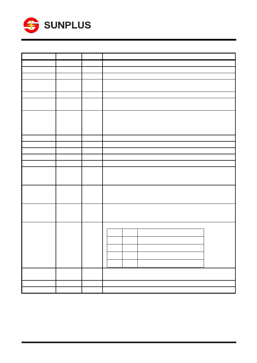
4. SIGNAL DESCRIPTIONS
Mnemonic
PIN No.
Type
Description
VDD
19, 20, 28
I
Logic Power input
VSS
11, 12, 37
I
Ground
VPP
23, 24
I
LCD Voltage; V
LCD
= VPP - VSS
V2
V3
22
21
I
LCD Bias Voltage Control.
Open for 1/5 Bias, Short for 1/4 Bias
E
27
I
It is a start signal to read data or write data.
R / W
26
I
It is a signal to select read or write.
1: Read, 0: Write.
RS
25
I
It is a signal to select register.
1: Data register (for read and write)
0: Instruction register (for write),
Busy flag -- address counter (for read).
DB3 - DB0
32 - 29
I/O
Low-order 4 data bits
DB7 - DB4
36 - 33
I/O
High-order 4 data bits
SEG80 - SEG1
46 - 125
O
Segment signals for LCD.
COM16 - COM9
45 - 38
O
Common signals for LCD.
COM8 - COM1
1 - 8
O
Common signals for LCD.
TYPE
14
I
LCD Alternate Signals.
TYPE = 0: Type-A
TYPE = 1: Type-B
DIRC
15
I
Common Scan Direction
DIRC = 0: COM1 COM2 ... COM15 COM16
DIRC = 1: COM16 COM15 ... COM2 COM1
SHL
16
I
Segment Shift Direction
SHL = 0: SEG1 SEG2 ... SEG79 SEG80
SHL = 1: SEG80 SEG79 ... SEG2 SEG1
MOD1
MOD0
18
17
I
CGROM / CGRAM Mode Select
MOD1
MOD0
Function
1
1
1
1
0
0
0
0
$00 - $0F as CGRAM
$00 - $07 as CGRAM, $08 - $0F as CGROM
$00 - $03 as CGRAM, $04 - $0F as CGROM
$00 - $0F as CGROM
OSC1
13
For internal clock operation, leave this pin open.
For external clock operation, the clock is input to OSC1.
CL2
10
O
Test Mode Clock Output; Open for normally use.
D
9
O
Test Mode Data Output; Open for normally use.
Sunplus Confidential
For PARTMINER Use Only