 | –≠–ª–µ–∫—Ç—Ä–æ–Ω–Ω—ã–π –∫–æ–º–ø–æ–Ω–µ–Ω—Ç: SPP1413A | –°–∫–∞—á–∞—Ç—å:  PDF PDF  ZIP ZIP |
2005/10/31
Ver.2
Page 1
SPP1413A
P-Channel Enhancement Mode MOSFET
DESCRIPTION
APPLICATIONS
The SPP1413A is the P-Channel logic enhancement
mode power field effect transistors are produced using
high cell density , DMOS trench technology.
This high density process is especially tailored to
minimize on-state resistance.
These devices are particularly suited for low voltage
application such as cellular phone and notebook
computer power management and other battery powered
circuits where high-side switching , and low in-line
power loss are needed in a very small outline surface
mount package.
Power Management in Note book
Portable Equipment
Battery Powered System
DC/DC Converter
Load Switch
DSC
LCD Display inverter
FEATURES
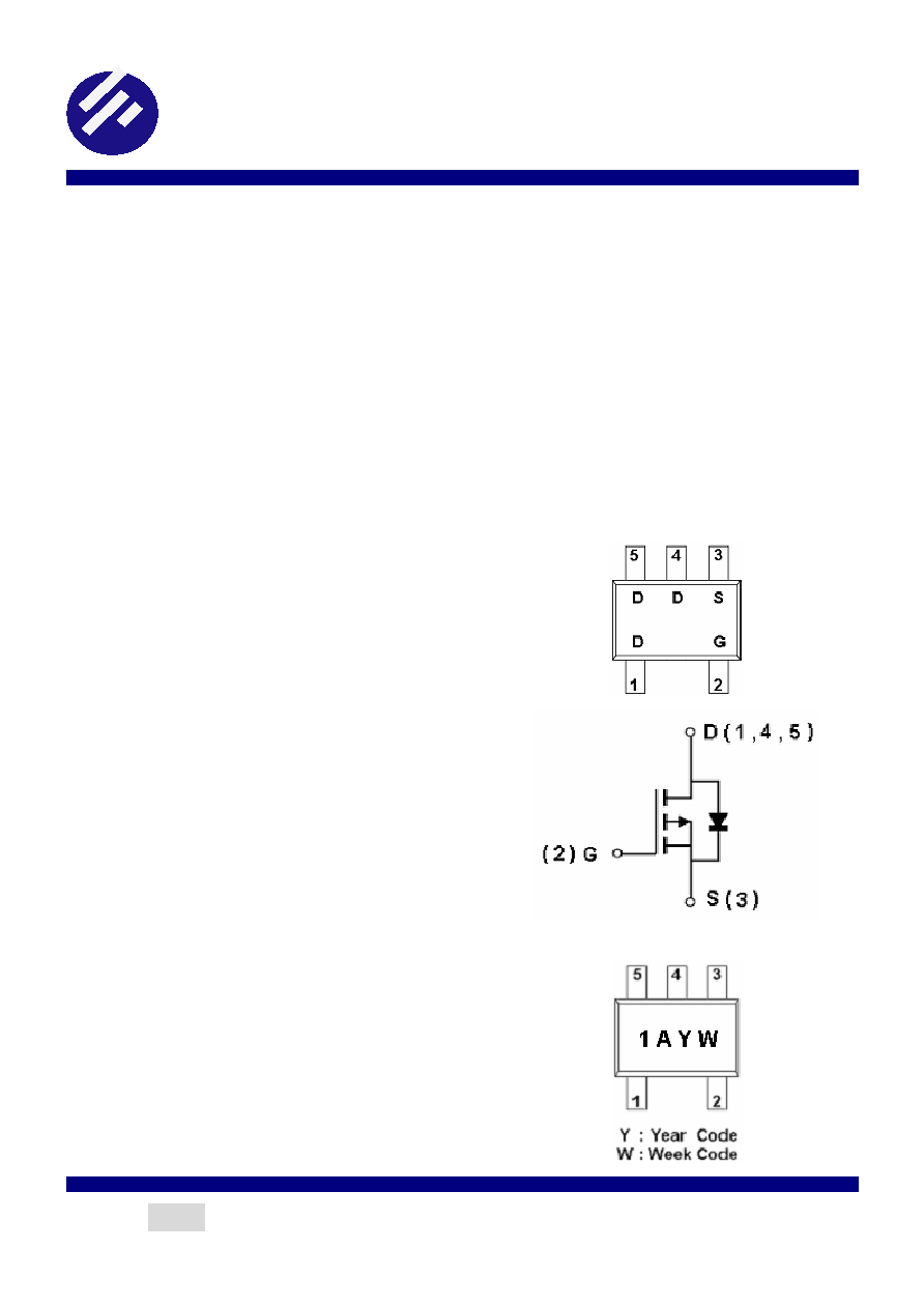
PIN CONFIGURATION ( SOT-353 ; SC-70 )
PART MARKING
-20V/-3.4A,R
DS(ON)
= 130m@V
GS
=-4.5V
-20V/-2.4A,R
DS(ON)
= 150m@V
GS
=-2.5V
-20V/-1.7A,R
DS(ON)
= 190m@V
GS
=-1.8V
Super high density cell design for extremely low
RDS (ON)
Exceptional on-resistance and maximum DC
current capability
SOT-353 ( SC≠70 ) package design
2005/10/31
Ver.2
Page 2
SPP1413A
P-Channel Enhancement Mode MOSFET
PIN DESCRIPTION
Pin Symbol
Description
2 G Gate
3 S
Source
1 , 4 , 5
D
Drain
ORDERING INFORMATION
Part Number
Package
Part Marking
SPP1413AS35RG SOT-353
1AYW
Week Code : A ~ Z( 1 ~ 26 ) ; a ~ z( 27 ~ 52 )
SPP1413AS35RG : Tape Reel ; Pb ≠ Free
ABSOULTE MAXIMUM RATINGS
(T
A
=25 Unless otherwise noted)
Parameter Symbol
Typical
Unit
Drain-Source Voltage
V
DSS
-20
V
Gate ≠Source Voltage
V
GSS
±12
V
T
A
=25
-2.3
Continuous Drain Current(T
J
=150 )
T
A
=70
I
D
-1.7
A
Pulsed Drain Current
I
DM
-6 A
Continuous Source Current(Diode Conduction)
I
S
-1.4 A
T
A
=25
0.95
Power Dissipation
T
A
=70
P
D
0..51
W
Operating Junction Temperature
T
J
-55/150
Storage Temperature Range
T
STG
-55/150
Thermal Resistance-Junction to Ambient
R
JA
105
/W
2005/10/31
Ver.2
Page 3
SPP1413A
P-Channel Enhancement Mode MOSFET
ELECTRICAL CHARACTERISTICS
(T
A
=25 Unl
ess otherwise noted)
Parameter Symbol
Conditions
Min.
Typ
Max.
Unit
Static
Drain-Source Breakdown Voltage
V
(BR)DSS
V
GS
=0V,I
D
=-250uA -20
Gate Threshold Voltage
V
GS(th)
V
DS
=V
GS
,I
D
=-250uA -0.35 -0.8
V
Gate Leakage Current
I
GSS
V
DS
=0V,V
GS
=±12V
±100
nA
V
DS
=-20V,V
GS
=0V
-1
Zero Gate Voltage Drain Current
I
DSS
V
DS
=-20V,V
GS
=0V
T
J
=55
-5
uA
On-State Drain Current
I
D(on)
V
DS
-5V,V
GS
=-4.5V
-6 A
V
GS
=-4.5V,I
D
=-3.4A
0.110
0.130
V
GS
=-2.5V,I
D
=-2.4A
0.130
0.150
Drain-Source On-Resistance
R
DS(on)
V
GS
=-1.8V,I
D
=-1.7A
0.170
0.190
Forward Transconductance
gfs
V
DS
=-5V,I
D
=-2.8A
6
S
Diode Forward Voltage
V
SD
I
S
=-1.5A,V
GS
=0V
-0.8
-1.2
V
Dynamic
Total Gate Charge
Q
g
4.8
8
Gate-Source Charge
Q
gs
1.0
Gate-Drain Charge
Q
gd
V
DS
=-6V,V
GS
=-4.5V
I
D
-2.8A
1.0
nC
Input Capacitance
C
iss
485
Output Capacitance
C
oss
85
Reverse Transfer Capacitance
C
rss
V
DS
=-6V,V
GS
=0V
f=1MHz
40
pF
t
d(on)
10
16
Turn-On Time
t
r
13
23
t
d(off)
18
25
Turn-Off Time
t
f
V
DD
=-6V,R
L
=6
I
D
-1.0A,V
GEN
=-4.5V
R
G
=6
15 20
ns
2005/10/31
Ver.2
Page 4
SPP1413A
P-Channel Enhancement Mode MOSFET
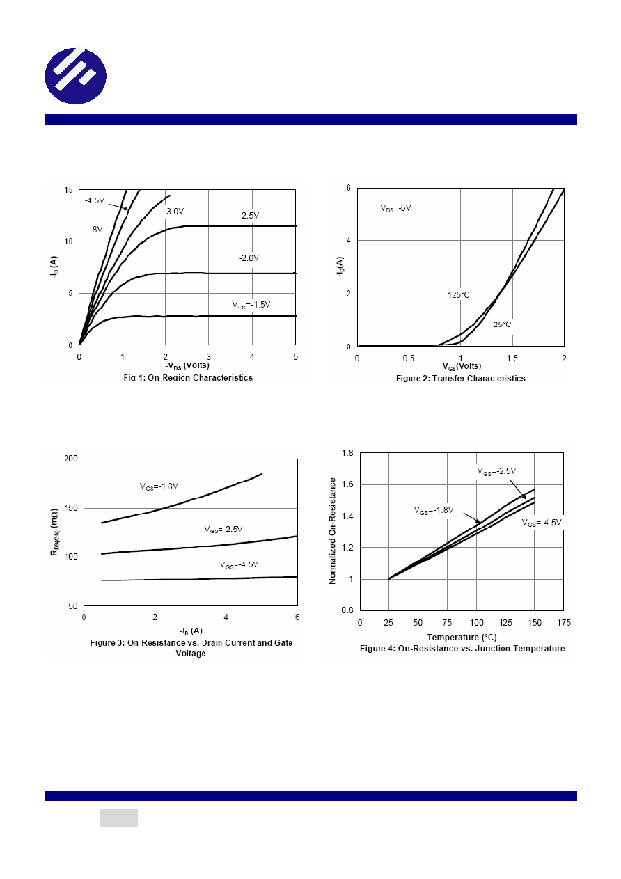
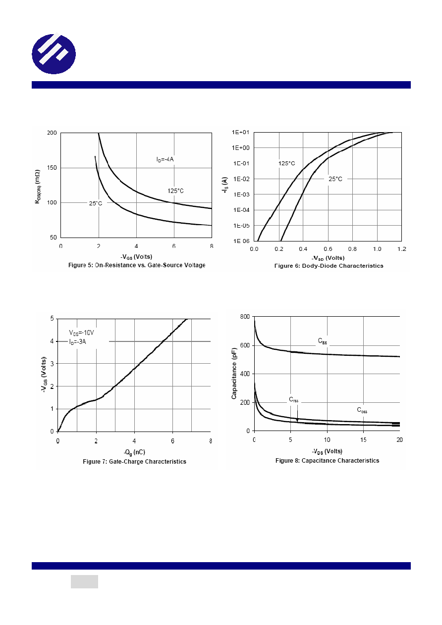
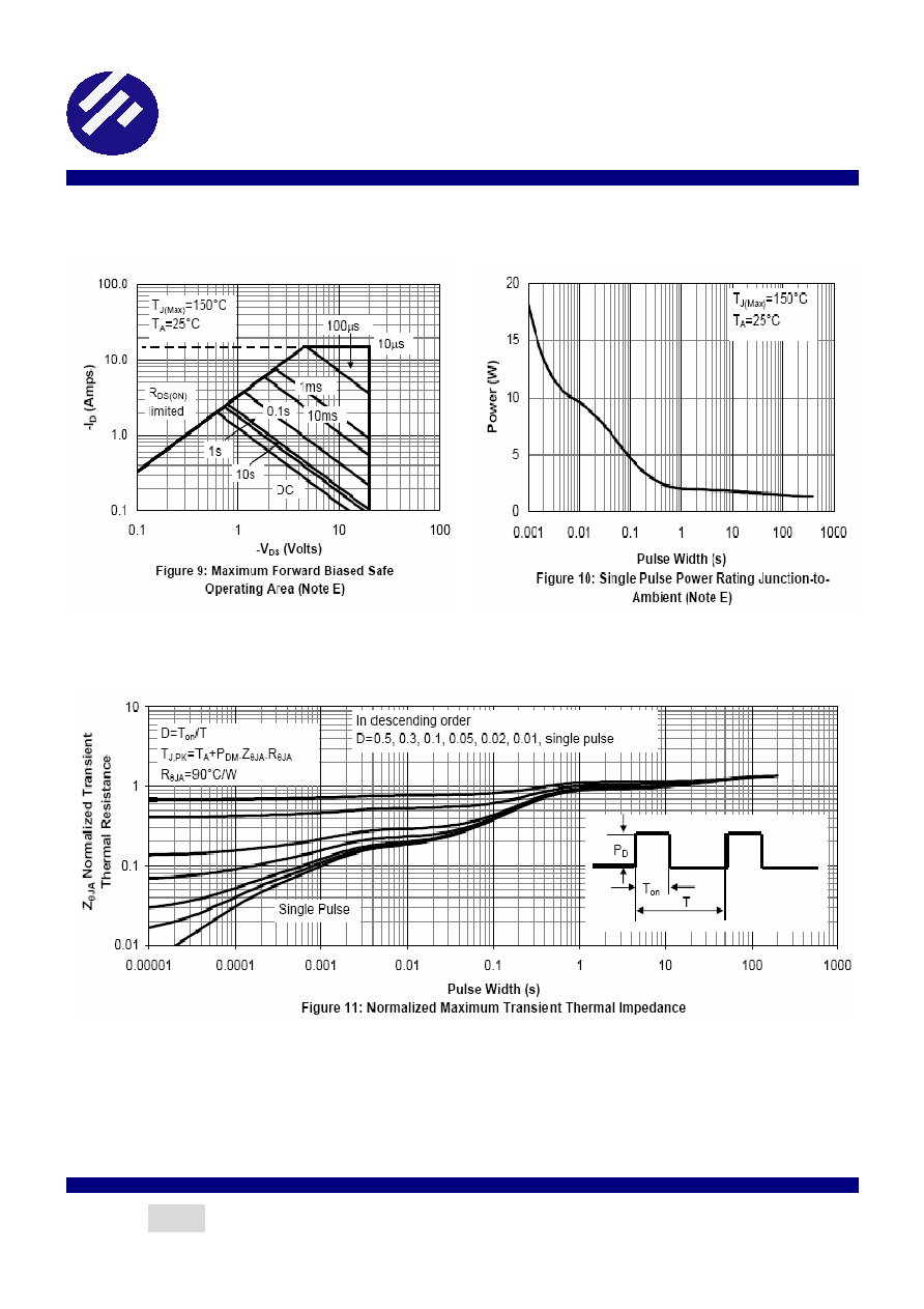
TYPICAL CHARACTERISTICS
2005/10/31
Ver.2
Page 5
SPP1413A
P-Channel Enhancement Mode MOSFET
TYPICAL CHARACTERISTICS
2005/10/31
Ver.2
Page 6
SPP1413A
P-Channel Enhancement Mode MOSFET
TYPICAL CHARACTERISTICS
2005/10/31
Ver.2
Page 7
SPP1413A
P-Channel Enhancement Mode MOSFET
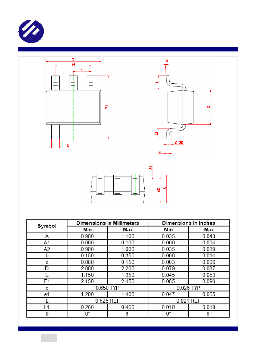
SOT-353 PACKAGE OUTLINE

2005/10/31
Ver.2
Page 8
SPP1413A
P-Channel Enhancement Mode MOSFET
Information provided is alleged to be exact and consistent. SYNC Power Corporation presumes no responsibility for the
penalties of use of such information or for any violation of patents or other rights of third parties which may result from its use.
No license is granted by allegation or otherwise under any patent or patent rights of SYNC Power Corporation. Conditions
mentioned in this publication are subject to change without notice. This publication surpasses and replaces all information
previously supplied. SYNC Power Corporation products are not authorized for use as critical components in life support
devices or systems without express written approval of SYNC Power Corporation.
©The SYNC Power logo is a registered trademark of SYNC Power Corporation
©2004 SYNC Power Corporation ≠ Printed in Taiwan ≠ All Rights Reserved
SYNC Power Corporation
9F-5, No.3-2, Park Street
NanKang District (NKSP), Taipei, Taiwan 115
Phone: 886-2-2655-8178
Fax: 886-2-2655-8468
©http://www.syncpower.com