 | ÐлекÑÑоннÑй компоненÑ: SSM9916J | СкаÑаÑÑ:  PDF PDF  ZIP ZIP |
Äîêóìåíòàöèÿ è îïèñàíèÿ www.docs.chipfind.ru
www.SiliconStandard.com 1 of 6
SSM9916H,J
N-CHANNEL ENHANCEMENT-MODE POWER MOSFET
Low on-resistance BV
DSS
18V
Capable of 2.5V gate drive R
DS(ON)
25m
Low drive current I
D
35A
Simple drive requirement
Description
Absolute Maximum Ratings
Symbol
Units
V
DS
V
V
GS
V
I
D
@
T
C
=25
°C
I
D
@
T
C
=125
°C
I
DM
A
P
D
@
T
C
=25
°C
W/
°C
T
STG
T
J
Symbol
Value
Unit
Rthj-c Thermal Resistance Junction-case Max. 2.5
°C/W
Rthj-a Thermal Resistance Junction-ambient Max. 110
°C/W
Thermal Data
Parameter
Storage Temperature Range
Total Power Dissipation 50
W
-55 to 150
°C
Operating Junction Temperature Range -55 to 150
°C
Linear Derating Factor
0.4
Continuous Drain Current, V
GS
@ 4.5V 16 A
Pulsed Drain Current
1
90
Gate-Source Voltage
Continuous Drain Current, V
GS
@ 4.5V 35 A
Parameter
Rating
Drain-Source Voltage
18
Power MOSFETs from Silicon Standard provide the
designer with the best combination of fast switching,
ruggedized device design, ultra low on-resistance and
cost-effectiveness.
± 12
G D
S
TO-252(H)
G
D
S
TO-251(J)
G
D
S
Rev.2.02 1/29/2004

www.SiliconStandard.com 2 of 6
SSM9916H,J
Electrical Characteristics
@ T
j
=25
o
C
(unless otherwise specified)
Symbol
Parameter
Test Conditions
Min.
Typ. Max. Units
BV
DSS
Drain-Source Breakdown Voltage
V
GS
=0V, I
D
=250uA
18
-
-
V
BV
DSS
/
T
j
Breakdown Voltage Temperature Coefficient
Reference to 25°C, I
D=1mA - 0.03 - V/
°C
R
DS(ON)
Static Drain-Source On-Resistance V
GS
=4.5V, I
D
=6A - - 25
m
V
GS
=2.5V, I
D
=5.2A - - 40
m
V
GS(th)
Gate Threshold Voltage
V
DS
=V
GS
, I
D
=250uA
0.5
-
1
V
g
fs
Forward Transconductance
V
DS
=10V, I
D
=6A
-
18
-
S
I
DSS
Drain-Source Leakage Current (T
j
=25
o
C)
V
DS
=18V, V
GS
=0V
-
-
1
uA
Drain-Source Leakage Current (T
j
=125
o
C)
V
DS
=18V ,V
GS
=0V
-
-
25
uA
I
GSS
Gate-Source Leakage
V
GS
=
-
-
nA
Q
g
Total Gate Charge
2
I
D
=18A
-
17.5
-
nC
Q
gs
Gate-Source Charge
V
DS
=18V
-
1.2
-
nC
Q
gd
Gate-Drain ("Miller") Charge
V
GS
=5V
-
7.9
-
nC
t
d(on)
Turn-on Delay Time
2
V
DS
=10V
-
7.3
-
ns
t
r
Rise Time I
D
=18A - 98 - ns
t
d(off)
Turn-off Delay Time R
G
=3.3
,
V
GS
=5V - 25.6 - ns
t
f
Fall Time R
D
=0.56
- 98 - ns
C
iss
Input Capacitance V
GS
=0V - 527 - pF
C
oss
Output Capacitance
V
DS
=18V
-
258
-
pF
C
rss
Reverse Transfer Capacitance
f=1.0MHz
-
112
-
pF
Source-Drain Diode
Symbol
Parameter
Test Conditions
Min.
Typ. Max. Units
I
S
Continuous Source Current ( Body Diode )
V
D
=V
G
=0V , V
S
=1.3V
-
-
35
A
I
SM
Pulsed Source Current ( Body Diode )
1
-
-
90
A
V
SD
Forward On Voltage
2
T
j
=25
°C, I
S
=35A, V
GS
=0V - - 1.3 V
Notes:
1.Pulse width limited by safe operating area.
2.Pulse width <300us , duty cycle <2%.
± 12V
±
100
Rev.2.02 1/29/2004
www.SiliconStandard.com 3 of 6
SSM9916H,J
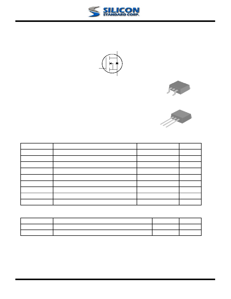
Fig 1. Typical Output Characteristics Fig 2. Typical Output Characteristics
Fig 3. On-Resistance vs. Gate Voltage Fig 4. Normalized On-Resistance
vs. Junction Temperature
0.6
0.8
1.0
1.2
1.4
1.6
1.8
-50
0
50
100
150
T
j
, Junction Temperature (
o
C)
No
rma
l
i
z
e
d
R
DS
(
ON)
V
G
=4.5V
I
D
=6A
0
20
40
60
80
100
0
1
2
3
4
5
6
7
V
DS
, Drain-to-Source Voltage (V)
I
D
,
Dra
i
n C
u
rre
nt
(A
)
T
C
=25
o
C
V
G
=1.5V
V
G
=2.5V
V
G
=4.5V
V
G
=3.5V
0
10
20
30
40
50
60
70
80
0
1
2
3
4
5
6
7
8
V
DS
, Drain-to-Source Voltage (V)
I
D
,
Dra
i
n C
u
rre
nt
(A
)
T
C
=150
o
C
V
G
=1.5V
V
G
=2.5V
V
G
=3.5V
V
G
=4.5V
18
20
22
24
26
28
30
1
2
3
4
5
6
V
GS
(V)
R
DS
ON
(m
)
I
D
= 6 A
T
C
=25
o
C
Rev.2.02 1/29/2004
www.SiliconStandard.com 4 of 6
SSM9916H,J
Fig 5. Maximum Drain Current vs. Fig 6. Typical Power Dissipation
Case Temperature
Fig 7. Maximum Safe Operating Area Fig 8. Effective Transient Thermal Impedance
0
10
20
30
40
50
60
0
50
100
150
T
c
, Case Temperature (
o
C)
P
D
(W
)
0
5
10
15
20
25
30
35
40
25
50
75
100
125
150
T
c
, Case Temperature (
o
C)
I
D
,
Dra
i
n C
u
rre
nt
(A
)
0.01
0.1
1
0.00001
0.0001
0.001
0.01
0.1
1
t , Pulse Width (s)
N
o
r
m
aliz
ed T
h
er
m
a
l Res
pon
s
e
(
R
th
jc
)
P
DM
Duty factor = t/T
Peak T
j
= P
DM
x R
thjc
+ T
C
t
T
0.02
0.01
0.05
0.1
0.2
DUTY=0.5
SINGLE PULSE
0.1
1
10
100
1000
0.1
1
10
100
V
DS
(V)
I
D
(A
)
T
c
=25
o
C
Single Pulse
10us
1ms
10ms
100ms
100us
Rev.2.02 1/29/2004
www.SiliconStandard.com 5 of 6
SSM9916H,J
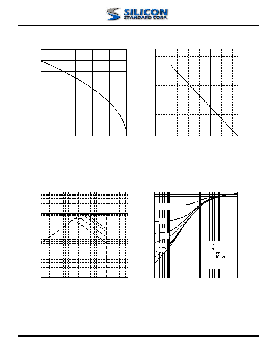
Fig 9. Gate Charge Characteristics Fig 10. Typical Capacitance Characteristics
Fig 11. Forward Characteristic of Fig 12. Gate Threshold Voltage vs.
Reverse Diode
Junction Temperature
0.2
0.45
0.7
0.95
1.2
-50
0
50
100
150
T
j
, Junction Temperature (
o
C )
V
GS
(t
h
)
(V)
0.01
0.1
1
10
100
0
0.4
0.8
1.2
1.6
V
SD
(V)
I
S
(A
)
T
j
=25
o
C
T
j
=150
o
C
10
100
1000
1
5
9
13
17
21
25
V
DS
(V)
C (
p
F)
f=1.0MHz
Ciss
Coss
Crss
0
2
4
6
8
10
12
14
16
0
5
10
15
20
25
30
35
40
45
Q
G
, Total Gate Charge (nC)
V
GS
, Ga
te to
So
urce Vo
lta
g
e
(
V
)
I
D
=18A
V
DS
=15V
V
DS
=18V
V
DS
=10V
Rev.2.02 1/29/2004