www.SiliconStandard.com 1 of 6
SSM9926M
DUAL N-CHANNEL ENHANCEMENT-MODE POWER MOSFETS
Low on-resistance BV
DSS
20V
Capable of 2.5V gate drive R
DS(ON)
30m
Low drive current I
D
6A
Surface-mount package
Description
Absolute Maximum Ratings
Symbol Units
V
DS
V
V
GS
V
I
D
@
T
A
=25
�C
I
D
@
T
A
=70
�C
I
DM
A
P
D
@
T
A
=25
�C
W/
�C
T
STG
T
J
Symbol Value Unit
Rthj-a Thermal Resistance Junction-ambient Max. 62.5
�C/W
Thermal Data
Parameter
Storage Temperature Range
Total Power Dissipation 2
W
-55 to 150
�C
Operating Junction Temperature Range -55 to 150
�C
Linear Derating Factor 0.016
Continuous Drain Current
3
, V
GS
@ 4.5V 4.8 A
Pulsed Drain Current
1,4
20
Gate-Source Voltage
Continuous Drain Current
3
, V
GS
@ 4.5V 6 A
Parameter Rating
Drain-Source Voltage 20
Power MOSFETs from
Silicon Standard provide the
designer with the best combination of fast switching,
ruggedized device design, ultra low on-resistance and
cost-effectiveness.
�
8
S1
G1
S2
G2
D1
D1
D2
D2
SO-8
G2
D2
S2
G1
D1
S1
Rev.2.01 6/26/2003
www.SiliconStandard.com 2 of 6
SSM9926M
Electrical Characteristics
@ T
j
=25
o
C
(unless otherwise specified)
Symbol Parameter Test Conditions Min. Typ. Max. Units
BV
DSS
Drain-Source Breakdown Voltage V
GS
=0V, I
D
=250uA 20 - - V
BV
DSS
/
T
j
Breakdown Voltage Temperature Coefficient
Reference to 25
�C, I
D
=1mA - 0.03 - V/
�C
R
DS(ON)
Static Drain-Source On-Resistance V
GS
=4.5V, I
D
=6A - - 30
m
V
GS
=2.5V, I
D
=5.2A - - 40
m
V
GS(th)
Gate Threshold Voltage V
DS
=V
GS
, I
D
=250uA 0.5 - 1.2 V
g
fs
Forward Transconductance V
DS
=10V, I
D
=6A - 17 - S
I
DSS
Drain-Source Leakage Current (T
j
=25
o
C)
V
DS
=20V, V
GS
=0V - - 1 uA
Drain-Source Leakage Current (T
j
=70
o
C)
V
DS
=20V ,V
GS
=0V - - 25 uA
I
GSS
Gate-Source Leakage V
GS
=
-
-
nA
Q
g
Total Gate Charge
2
I
D
=6A - 18 - nC
Q
gs
Gate-Source Charge V
DS
=20V - 1.1 - nC
Q
gd
Gate-Drain ("Miller") Charge V
GS
=5V - 7.4 - nC
t
d(on)
Turn-on Delay Time
2
V
DS
=10V - 7.2 - ns
t
r
Rise Time I
D
=1A - 12.8 - ns
t
d(off)
Turn-off Delay Time R
G
=3.3
, V
GS
=5V
- 30.5 - ns
t
f
Fall Time R
D
=10
- 10.5 - ns
C
iss
Input Capacitance V
GS
=0V - 510 - pF
C
oss
Output Capacitance V
DS
=20V - 245 - pF
C
rss
Reverse Transfer Capacitance f=1.0MHz - 110 - pF
Source-Drain Diode
Symbol Parameter Test Conditions Min. Typ. Max. Units
V
SD
Forward On Voltage
2
T
j
=25
�C, I
S
=1.7A, V
GS
=0V - - 1.2 V
Notes:
1.Pulse width limited by Max. junction temperature.
2.Pulse width <300us , duty cycle <2%.
3.Surface mounted on FR4 board, t<10 sec.
4.Pulse width <10us , duty cycle <1%.
�
8V
�
100
Rev.2.01 6/26/2003
www.SiliconStandard.com 3 of 6
SSM9926M
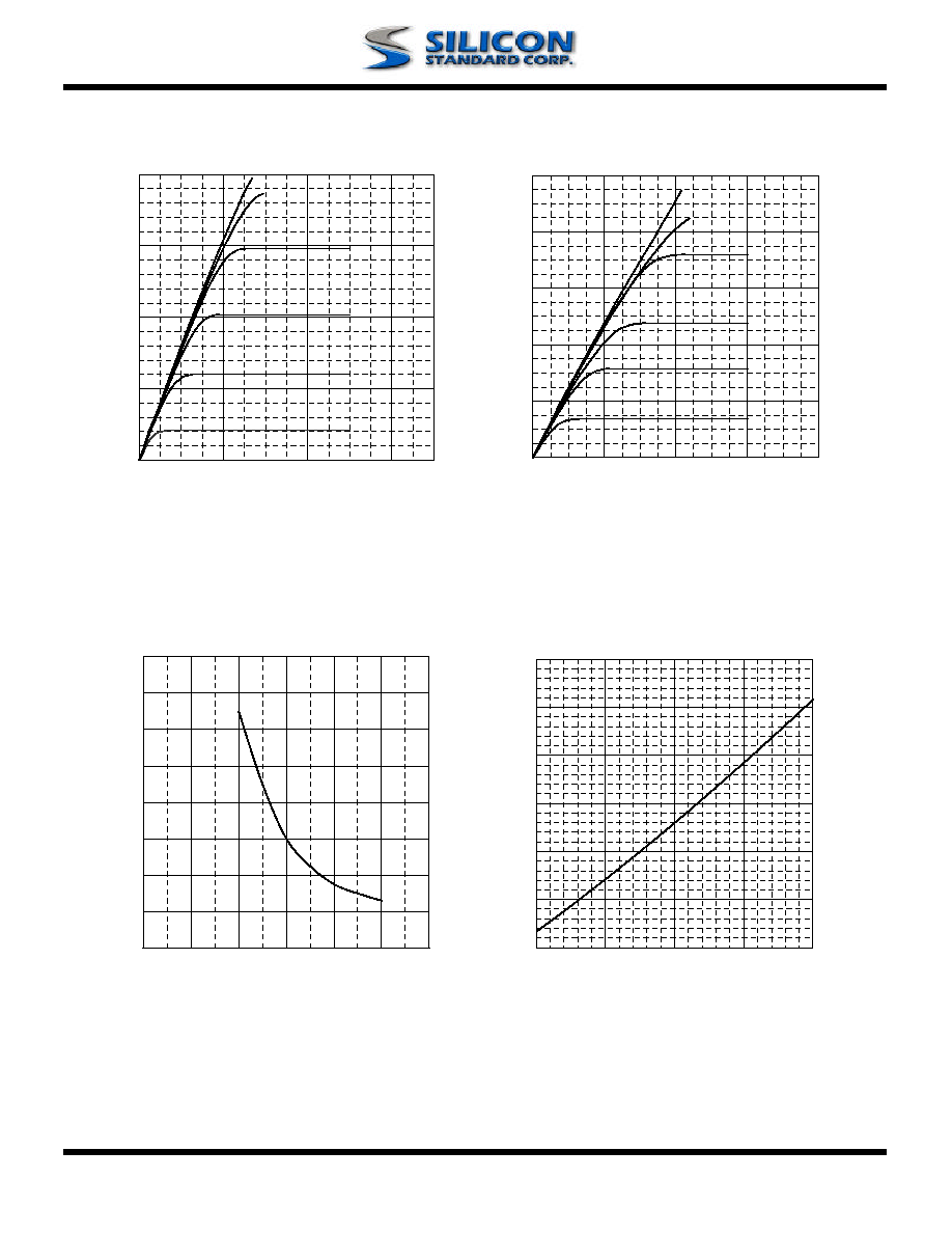
Fig 1. Typical Output Characteristics Fig 2. Typical Output Characteristics
Fig 3. On-Resistance vs. Gate Voltage Fig 4. Normalized On-Resistance
vs. Junction Temperature
0.6
0.8
1.0
1.2
1.4
1.6
1.8
-50 0 50 100 150
T
j
, Junction Temperature (
o
C)
N
o
rm
a
li
z
e
d
R
D
S
(
ON)
V
G
=4.5V
I
D
=6A
22
24
26
28
30
32
34
36
38
0
1
2
3
4
5
6
V
GS
(V)
R
D
S
ON
I
D
=6A
T
C
=25
o
C
0
5
10
15
20
0 0.4 0.8 1.2
V
DS
, Drain-to-Source Voltage (V)
I
D
,
Dr
a
i
n
C
u
rr
e
nt
(
A
)
T
C
=25
o
C
V
G
=1.5V
V
G
=2.0V
V
G
=2.5V
V
G
=3.0V
V
G
=4.5V
V
G
=3.5V
0
4
8
12
16
20
0 0.4 0.8 1.2 1.6
V
DS
, Drain-to-Source Voltage (V)
I
D
,
Dr
a
i
n
C
u
rr
e
nt
(
A
)
T
C
=150
o
C
V
G
=1.5V
V
G
=2.0V
V
G
=2.5V
V
G
=3.5V
V
G
=4.5V
V
G
=3.0V
Rev.2.01 6/26/2003
www.SiliconStandard.com 4 of 6
SSM9926M
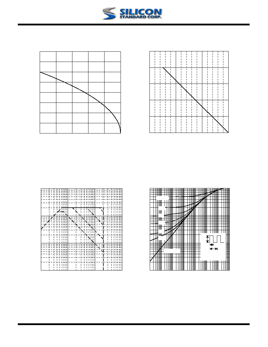
Fig 5. Maximum Drain Current vs. Fig 6. Typical Power Dissipation
Case Temperature
Fig 7. Maximum Safe Operating Area Fig 8. Effective Transient Thermal Impedance
0
1
2
3
4
5
6
7
8
25 50 75 100 125 150
T
c
, Case Temperature (
o
C)
I
D
,
Dr
a
i
n
C
u
rr
e
nt
(
A
)
0
0.5
1
1.5
2
2.5
0 50 100 150
T
c
, Case Temperature (
o
C)
P
D
(
W
)
0.001
0.01
0.1
1
0.0001 0.001 0.01 0.1 1 10 100 1000
t , Pulse Width (s)
N
o
rm
a
li
z
ed
Therm
a
l
R
e
s
po
n
se (R
t
h
ja
)
P
DM
Duty factor = t/T
Peak T
j
= P
DM
x R
thja
+ T
a
t
T
0.02
0.01
0.05
0.1
0.2
DUTY=0.5
SINGLE PULSE
0.1
1
10
100
0.1 1 10 100
V
DS
(V)
I
D
(
A
)
T
c
=25
o
C
Single Pulse
1s
1ms
10ms
100ms
Rev.2.01 6/26/2003
www.SiliconStandard.com 5 of 6
SSM9926M
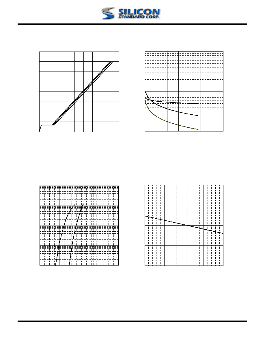
Fig 9. Gate Charge Characteristics Fig 10. Typical Capacitance Characteristics
Fig 11. Forward Characteristic of Fig 12. Gate Threshold Voltage vs.
Reverse Diode
Junction Temperature
0.2
0.45
0.7
0.95
1.2
-50 0 50 100 150
T
j
, Junction Temperature (
o
C )
V
G
S
(
t
h
)
(V)
0.01
0.1
1
10
100
0 0.4 0.8 1.2 1.6
V
SD
(V)
I
S
(
A
)
T
j
=25
o
C
T
j
=150
o
C
0
2
4
6
8
10
12
14
16
0 5 10 15 20 25 30 35 40 45
Q
G
, Total Gate Charge (nC)
V
GS
,
G
a
te to
S
o
u
r
ce Voltage
(
V)
V
DS
=10V
V
DS
=15V
V
DS
=20V
Id=6A
100
1000
10000
1
5
9
13
17
21
25
29
V
DS
(V)
C
(
p
F)
f=1.0MHz
Ciss
Coss
Crss
Rev.2.01 6/26/2003