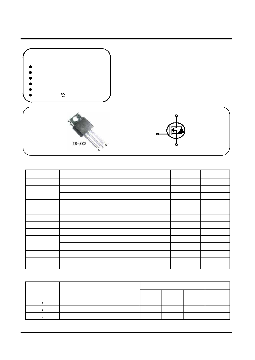
SAMWIN
SW4N60
REV0.1
04.10.15
General Description
This power MOSFET is produced in CHMC with
advanced VDMOS technology of SAMWIN. This
technology enable power MOSFET to have better
characteristics, such as fast switching time, low on
resistance, low gate charge and especially excellent
avalanche characteristics. This power MOSFET is
usually used at high efficient DC to DC converter
block and high efficiency switch mode power
supplies.
Features
N-Channel MOSFET
BV
DSS
(Minimum)
R
DS(ON)
(Maximum)
I
D
Qg (Typical)
P
D
(@TC=25
)
: 600 V
: 2.2 ohm
: 4.0 A
: 20 nc
: 73 W
G
S
D
Absolute Maximum Ratings
Symbol
Parameter
Value
Units
V
DSS
Drain to Source Voltage
600
V
Continuous Drain Current (@Tc=25
)
4
A
Continuous Drain Current (@Tc=100
)
3.0
A
I
DM
Drain Current Pulsed
(Note 1)
16
A
V
GS
Gate to Source Voltage
�
30
V
E
AS
Single Pulsed Avalanche Energy
(Note 2)
260
mJ
E
AR
Repetitive Avalanche Energy
(Note 1)
7.3
mJ
dv/dt
Peak Diode Recovery dv/dt
(Note 3)
4.5
V/ns
Total Power Dissipation (@Tc=25
)
73
W
Derating Factor above 25
0.85
W/
T
STG
,T
J
Operating junction temperature &Storage temperature
-55~+150
T
L
Maximum Lead Temperature for soldering purpose, 1/8 from Case
for 5 seconds.
300
P
D
I
D
Thermal Characteristics
/ W
62.5
-
-
Thermal Resistance, Junction-to-Ambient
R
JA
/ W
-
0.5
-
Thermal Resistance, Case-to-Sink
R
CS
/ W
1.72
-
-
Thermal Resistance, Junction-to-Case
R
JC
Max
Typ
Min
Units
Value
Parameter
Symbol
1/6
SAMWIN
SW4N60
REV0.1
04.10.15
Electrical Characteristics
(Tc=25
unless otherwise noted)
Value
Symbol
Parameter
Test Conditions
Min
Typ
Max
Off Characteristics
BV
DSS
Drain- Source Breakdown Voltage
V
GS
=0V,I
D
=250uA
600
-
-
V
BV
DSS
/
Tj
Breakdown Voltage Temperature
coefficient
I
D
=250uA,referenced to 25
-
0.6
-
V/
V
DS
=600V, V
GS
=0V
I
DSS
Drain-Source Leakage Current
V
DS
=480V, Tc=125
-
-
1
uA
Gate-Source Leakage Current
V
GS
=30V,V
DS
=0V
-
-
100
nA
Gate-Source Leakage Reverse
V
GS
=-30V, V
DS
=0V
-
-
-100
nA
On Characteristics
V
GS
(th)
Gate Threshold Voltage
V
DS
=V
GS
,I
D
=250uA
2.0
-
4.0
V
R
DS(ON)
Static Drain-Source On-state
Resistance
V
GS
=10V,I
D
=2.0A
-
1.9
2.2
ohm
Dynamic Characteristics
Ciss
Input Capacitance
-
-
670
Coss
Output Capacitance
-
-
90
Crss
Reverse Transfer Capacitance
-
-
11
Dynamic Characteristics
t
d(on)
Turn-on Delay Time
-
-
60
t
r
Rise Time
-
-
94
t
d(off)
Turn-off Delay Time
-
-
140
t
f
Fall Time
-
-
74
Q
g
Total Gate Charge
-
20
30
Q
gs
Gate-Source Charge
-
5
-
Q
gd
Gate-Drain Charge (Miller Charge)
-
7
-
nc
V
DS
=480V,V
GS
=10V, I
D
=4.0A
(Note4,5)
ns
V
DD
=300V,I
D
=4.0A
R
G
=50ohm
(Note4,5)
pF
V
GS
=0V,V
DS
=25V, f=1MHz
I
GSS
Units
Source-Drain Diode Ratings and Characteristics
uc
-
1.5
-
Reverse Recovery Charge
Q
rr
ns
-
250
-
I
S
=1.0A,V
GS
=0V,
dI
F
/dt=100A/us
Reverse Recovery Time
t
rr
V
1.4
-
-
I
S
=1.0A,V
GS
=0V
Diode Forward Voltage
V
SD
16.0
-
-
Pulsed Source Current
I
SM
A
4.0
-
-
Integral Reverse
p-n Junction Diode
in the MOSFET
Continuous Source Current
I
S
Unit.
Max.
Typ.
Min.
Test Conditions
Parameter
Symbol
G
S
D
s
NOTES
1. Repeativity rating: pulse width limited by junction temperature
2. L=30mH,I
AS
=4.0A,V
DD
=50V,R
G
=0ohm, Starting TJ=25
3. I
SD
1.8A,di/dt
100A/us,V
DD
BVDSS, Starting TJ=25
4. Pulse Test: Pulse Width
300us,Duty Cycle
2%
5. Essentially independent of operating temperature.
2/6
SAMWIN
SW4N60
REV0.1
04.10.15
3/6
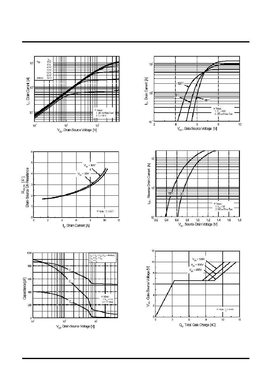
Fig 1. On-State Characteristics
Fig 3. On Resistance Variation vs.
Drain Current and Gate Voltage
Fig 4. On State Current vs.
Allowable Case Temperature
Fig 2. Transfer Characteristics
Fig 6. Gate Charge Characteristics
Fig 5. Capacitance Characteristics
(Non-Repetitive)
SAMWIN
SW4N60
REV0.1
04.10.15
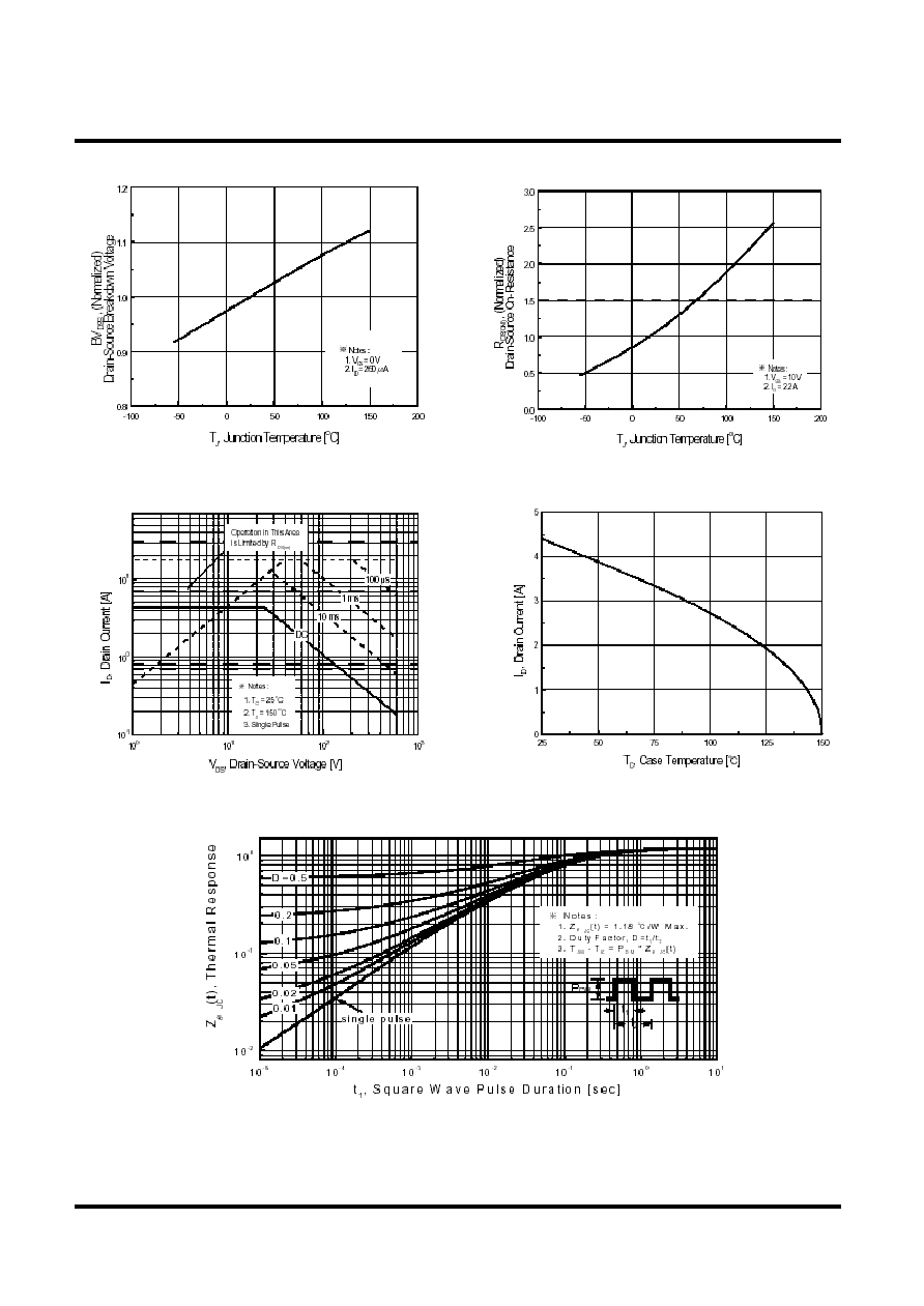
Fig 7. Breakdown Voltage Variation vs.
Junction Temperature
Fig 8. On-Resistance Variation vs.
Junction Temperature
Fig 10. Maximum Drain Current
Vs. Case Temperature
Fig9. Maximum Safe Operating
Fig 11. Transient Thermal Response Curve
4/6
SAMWIN
SW4N60
REV0.1
04.10.15
Time
V
DS
(t)
Q
gd
Q
gs
V
GS
10V
Charge
Q
g
DUT
1mA
Same Type
as DUT
200nF
50K
300nF
V
GS
V
DS
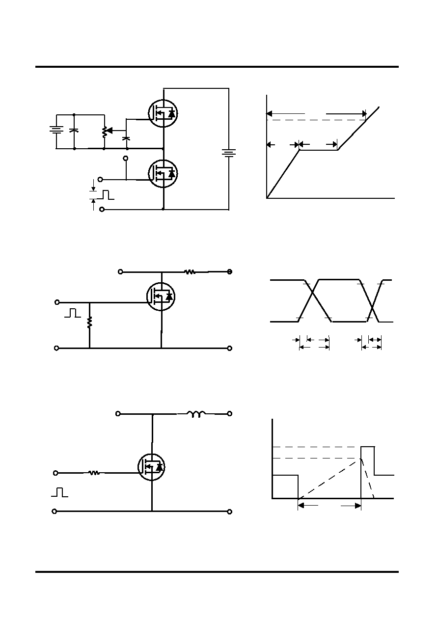
Fig 12. Gate Charge test Circuit & Waveforms
Fig 14. Unclamped Inductive Switching test Circuit & Waveforms
Fig 13. Switching test Circuit & Waveforms
V
DD
(0.5 rated V
DS
)
V
DS
V
in
90%
10%
t
d(on)
t
r
t
on
t
d(off)
t
f
t
off
V
DS
10V
R
G
DUT
R
L
Pulse
Generator
V
DD
t
p
V
DS
L
R
G
DUT
10V
BV
DSS
I
AS
I
D
(t)
V
DD
EAS= --- L
L
I
AS
2
---------------
BV
DSS
BV
DSS
-V
DD
1
2
5/6