 | –≠–ª–µ–∫—Ç—Ä–æ–Ω–Ω—ã–π –∫–æ–º–ø–æ–Ω–µ–Ω—Ç: T73227 | –°–∫–∞—á–∞—Ç—å:  PDF PDF  ZIP ZIP |

October 2002
This document contains information on a preproduction product. Specifications and information herein are subject to change without notice.
10.29.02
T73227
27 MHz VCXO Clock Generator IC
ISO9001
1.0 Features
∑
One-chip tunable voltage controlled crystal oscillator
(VCXO) allows precise system frequency tuning
∑
3.3V operation
∑
8 pin SOIC and MSOP packages
∑
Uses inexpensive 20pF pullable crystals with no
external capacitors required.
∑
12mA drive capability at TTL levels
2.0 Applications
∑
Set-top boxes
∑
MPEG Video clock source
∑
Oscillator replacement
3.0 Description
The T73227 is a single-chip, low-jitter Voltage-Controlled-
Crystal-Oscillator. The device accepts a 27 MHz, 20 pF
crystal, and produces a low jitter output at the same fre-
quency. A 0 to 3.0V control signal is used to fine tune the
output clock frequency in the ±100ppm range. This finds
use in systems that have frequency matching require-
ments, such as digital satellite receivers.
Figure 1: Block Diagram
CLK
VDD2
VDD1
X2
Load Cap Control
Output
Buffer
Load
Caps
27 MHz
Pullable
Crystal
VIN
X1
GND1
GND2
Oscillator

October 2002
2
10.29.02
ISO9001
T73227
27 MHz VCXO Clock Generator IC
Table 1: Pin Descriptions
PIN TYPE NAME
DESCRIPTION
1
Xi
X1
Crystal Connection. Connect to a 27 MHz Pullable Crystal
2 P
VDD1
Core
V
DD
. Connect to 3.3V
3
I
VIN
Voltage input to VCXO. Zero to 3.3V Signal Controls the Frequency of the
VCXO.
4
P
GND2
Connect to Ground.
5
O
CLK
Clock Output
6
P
VDD2
Pad Driver V
DD
. Connect to 3.3V
7
P
GND1
Connect to Ground.
8
Xi
X2
Crystal Connection. Connect to a 27 MHz pullable crystal.
Legend: I = Input
O = Output
P = Power supply connection
Xi = Crystal connections.
1
2
3
4
8
7
6
5
X1
VDD1
VIN
GND2
X2
GND1
VDD2
CLK
8-pin SOIC/MSOP

October 2002
3
10.29.02
ISO9001
T73227
27 MHz VCXO Clock Generator IC
4.0 Functional Block Description
The VCXO provides a tunable, low-jitter frequency reference. Loading capacitance for the crystal is internal to the
T73227. No external components (other than the crystal resonator itself) are required for operation of the VCXO.
Tuning of the VCXO frequency is accomplished by varying the voltage on Vin (Pin 3).
The oscillator operates the crystal resonator in the parallel-resonant mode. Crystal warping, or the "pulling" of the crys-
tal oscillation frequency, is accomplished by altering the effective load capacitance presented to the crystal by the os-
cillator circuit. The actual amount that changing the load capacitance alters the oscillator frequency will be dependent
on the characteristics of the crystal as well as the oscillator circuit itself.
Specifically, the motional capacitance of the crystal (usually referred to by crystal manufacturers as C
1
), the static ca-
pacitance of the crystal (C
0
), and the load capacitance (C
L
) of the oscillator determine the "warping" or "pulling"
capability of the crystal in the oscillator circuit. A simple
formula to obtain the warping capability of a crystal oscil-
lator is:
(
)
(
) (
)
C
C
C
C
C
C
C
ppm
f
L
L
L
L
1
0
2
0
6
1
2
1
2
10
)
(
+
◊
+
◊
◊
-
◊
=
where C
L1
and C
L2
are the two extremes of the applied
load capacitance.
EXAMPLE: A crystal with the following parameters is
used. With C
1
= 0.025pF, C
0
= 6pF, C
L1
= 10pF, and C
L2
= 20pF, the tuning range is
(
)
(
) (
)
ppm
.
f
300
10
6
20
6
2
106
10
20
025
0
=
+
◊
+
◊
◊
-
◊
=
.
5.0 Electrical
Specifications
Table 2: Absolute Maximum Ratings
Stresses above those listed under Absolute Maximum Ratings may cause permanent damage to the device. These conditions represent a stress rating only, and functional operation of the device at
these or any other conditions above the operational limits noted in this specification is not implied. Exposure to maximum rating conditions for extended conditions may affect device performance,
functionality, and reliability.
PARAMETER SYMBOL
MIN.
MAX.
UNITS
Supply Voltage (V
SS
= ground)
V
DD
V
SS
-0.5 5
V
Input Voltage, dc
V
I
V
SS
-0.5 V
DD
+0.5 V
Output Voltage, dc
V
O
V
SS
-0.5 V
DD
+0.5 V
Input Clamp Current, dc (V
I
< 0 or V
I
> V
DD
) I
IK
-25 25 mA
Output Clamp Current, dc (V
I
< 0 or V
I
> V
DD
) I
OK
-50 50 mA
Storage Temperature Range (non-condensing)
T
S
-65 150 ∞C
Ambient Temperature Range, Under Bias
T
A
-55 125 ∞C
Junction Temperature
T
J
125
∞C
Lead Temperature (soldering, 10s)
260
∞C
Input Static Discharge Voltage Protection
2
KV
T73227 Typical VCXO Deviation vs. Vin
-150
-100
-50
0
50
100
150
0.1
0.4
0.7
0.9
1.2
1.5
1.8
2.0
2.3
2.5
2.7
Vin
Deviation From 27 MHz ppm

October 2002
4
10.29.02
ISO9001
T73227
27 MHz VCXO Clock Generator IC
Table 3: Operating Conditions
PARAMETER SYMBOL
CONDITIONS/DESCRIPTION
MIN.
TYP.
MAX.
UNITS
Core Supply Voltage (V
DD
) V
DD
3.15 3.3 3.45 V
VCXO Control Voltage, V
IN
V
IN
0
V
DD
V
Ambient Operating Temperature Range
T
A
0
70 ∞C
Crystal Resonator Frequency
f
XTAL
Fundamental
Mode
20 27 30 MHz
Crystal Load Capacitance
C
L(xtal)
AT
cut
20
pF
Table 4: DC Electrical Specifications
Unless otherwise stated, V
DD
= 3.15V to 3.45V , no load on any output, and ambient temperature range T
A
= 0∞C to 70∞C.
PARAMETER SYMBOL
CONDITIONS/DESCRIPTION
MIN.
TYP.
MAX.
UNITS
Overall
Supply Current, Dynamic, with no load
I
DD
f
XTAL
= 27MHz
25
mA
Output High Voltage
V
OH
I
OH
= -12mA
2.4
V
Output Low Voltage
V
OL
I
OL
= 12mA
0.4
V
Voltage Controlled Crystal Oscillator - VDD=3.3V
Crystal Loading Capacitance
C
L(xtal)
As seen by a crystal connected to XIN and
XOUT (@ V
XTUNE
= 1.65V)
20 pF
Crystal Gamma
C
O
/C
1
240
VCXO Tuning Range
f
XTAL
= 27MHz; C
L(xtal)
= 20pF; gamma = 240
250 ppm
VCXO Tuning Characteristic
Note: positive
F for positive
V
75
ppm/V
Crystal ESR
50
Table 5: AC Timing Specifications
Unless otherwise stated, V
DD
= 3.15V to 3.45V, no load on any output, and ambient temperature range T
A
= 0∞C to 70∞C. Parameters denoted with an asterisk ( * ) represent nominal characterization
data and are not production tested to any specific limits.
PARAMETER SYMBOL CONDITIONS/DESCRIPTION MIN.
TYP.
MAX.
UNITS
Clock Output (CLK)
Duty Cycle *
Ratio of high pulse width (as measured from rising
edge to next falling edge at V
DD
/2) to one clock period
40 60 %
Jitter, Period (peak-peak) *
t
j(
P)
From rising edge to next rising edge at V
DD
/2, C
L
=
10pF
150
ps
Rise Time *
t
r
Measured 0.8V to 2.0V, C
L
= 10pF
1.5
ns
Fall Time *
t
f
Measured 2.0V to 0.8V; C
L
= 10pF
1.5
ns
October 2002
5
10.29.02
ISO9001
T73227
27 MHz VCXO Clock Generator IC
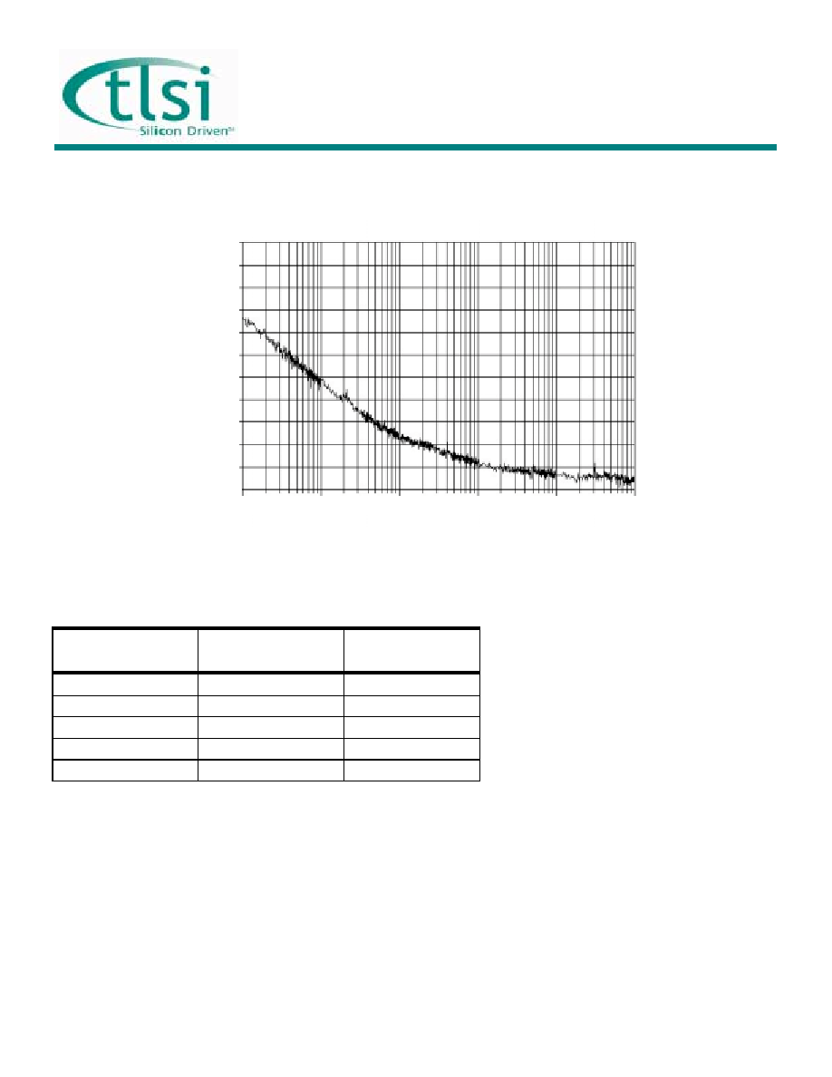
Phase Noise, dBc/Hz
Phase Noise vs. Frequency Offset
Frequency Offset from 27MHz
100 1K 10K 100K 1M
- 50
- 70
- 90
- 110
- 130
- 150
6.0 Ordering
Information
ORDERING PART
NUMBER
PACKAGE TYPE
SHIPPING
CONFIGURATION
T73227-S08
8-pin SOIC
Tubes
T73227-S08-TNR
8-pin SOIC
Tape and Reel
T73227-M08
8-pin MSOP
Tubes
T73227-M08-TNR
8-pin MSOP
Tape and Reel
T73227-DIE
DIE
Waffle-Pack
TLSI reserves the right to make changes to its products or to discontinue any product or service without notice, and advise customers to obtain the latest version of relevant information to verify,
before placing orders, that information being relied on is current and complete. All products are sold subject to the terms and conditions of sale supplied at the time of order acknowledgment, includ-
ing those pertaining to warranty, patent infringement, and limitation of liability.
TLSI warrants performance of its semiconductor products to the specifications applicable at the time of sale in accordance with TLSI's standard warranty. Testing and other quality control techniques
are utilized to the extent TLSI deems necessary to support this warranty. Specific testing of all parameters of each device is not necessarily performed, except those mandated by government
requirements.
Customers are responsible for their applications using TLSI devices.
Information furnished by TLSI is believed to be accurate and reliable. However, no responsibility is assumed by TLSI for its use, nor for any infringements of patents or other rights of third parties
which may result from its use. No license is granted by implication or otherwise under any patent rights of TLSI.
TLSI and Silicon Driven are trademarks of TLSI, Inc. All other trademarks are the property of their respective owners.
TLSI Incorporated, 770 Park Avenue, Huntington NY 11743
∑
∑
∑
∑
(631) 755-7005
∑
∑
∑
∑
Fax 631-755-7626
∑
∑
∑
∑
www.tlsi.com