
Product Information
ISO 9001 CERTIFIED
www.teledynewireless.com
email: amplifiers@teledyne.com
1274 Terra Bella Avenue, Mountain View, CA 94043 ∑ Tel: 800-832-6869 ∑ Fax: (650) 962-6845
10/2001
7
T
T
T
T
TA G - 1 0 3 0
A G - 1 0 3 0
A G - 1 0 3 0
A G - 1 0 3 0
A G - 1 0 3 0
5.725 to 5.825 GHz GaAs MMIC
5.725 to 5.825 GHz GaAs MMIC
5.725 to 5.825 GHz GaAs MMIC
5.725 to 5.825 GHz GaAs MMIC
5.725 to 5.825 GHz GaAs MMIC
U-NII Band Power Amplifier
U-NII Band Power Amplifier
U-NII Band Power Amplifier
U-NII Band Power Amplifier
U-NII Band Power Amplifier
F e a t u r
F e a t u r
F e a t u r
F e a t u r
F e a t u re s :
e s :
e s :
e s :
e s :
25 dBm Minimum Linear Output Power
25 dBm Minimum Linear Output Power
25 dBm Minimum Linear Output Power
25 dBm Minimum Linear Output Power
25 dBm Minimum Linear Output Power
20 dB Small Signal Gain
20 dB Small Signal Gain
20 dB Small Signal Gain
20 dB Small Signal Gain
20 dB Small Signal Gain
35 dBm 3
35 dBm 3
35 dBm 3
35 dBm 3
35 dBm 3
rd
rd
rd
rd
rd
Order Intercept Point
Order Intercept Point
Order Intercept Point
Order Intercept Point
Order Intercept Point
Surface Mount Thermally Efficient
Surface Mount Thermally Efficient
Surface Mount Thermally Efficient
Surface Mount Thermally Efficient
Surface Mount Thermally Efficient
Moly-Copper Package
Moly-Copper Package
Moly-Copper Package
Moly-Copper Package
Moly-Copper Package
Product Description
Product Description
Product Description
Product Description
Product Description
The TAG-1030 GaAs MMIC power amplifier is designed to operate in the ETSI approved Unlicensed band of 5.725 to
5.825 GHz. It provides a minimum of 20 dB gain, a minimum of +25 dBm linear output power when measured at 1 dB
GCP, and has an IP3 of +35 dBm. It is housed in a thermally efficient moly-copper surface mount package and is capable
of performing within typical commercial system operating temperature ranges.
Typical Small Signal Gain and Input Return Loss
-20
-10
0
10
20
30
5.70
5.75
5.80
5.85
5.90
Frequency (GHz)
Gain / Return Loss
(dB)
Gain
Return
Typical Output Power
22
23
24
25
26
27
28
29
30
5.70
5.75
5.80
5.85
5.90
5.95
Frequency (GHz)
Output Power (dBm)
P-1dB
Psat
Pa rame te r
Symbol
Fre que ncy
Min
Ma x
Typical
Units
Small Signal Gain
S
21
5.7 to 5.9 GHz
20.0
-
23.0
dB
Input Return Loss
S
11
5.7 to 5.9 GHz
-
-
-10.0
dB
Reverse Isolation
S
12
5.7 to 5.9 GHz
-
-
52.0
dB
5.7 GHz
25.0
-
26.0
dBm
Output Power @ 1dB Gain Compression P
-1dB
5.8 GHz
25.0
-
26.3
dBm
5.9 GHz
25.0
-
26.8
dBm
Temperature Coefficient of Gain
S
21
5.7 to 5.9 GHz
-
-
-0.045
dB/
o
C
Electrical Specifications
Electrical Specifications
Electrical Specifications
Electrical Specifications
Electrical Specifications
(All Specifications at 25
o
C, V
d
= +7.0V, I
d
= 500 to 700 mA)
www.teledynewireless.com
email: amplifiers@teledyne.com
1274 Terra Bella Avenue, Mountain View, CA 94043 ∑ Tel: 800-832-6869 ∑ Fax: (650) 962-6845
10/2001
8
T
T
T
T
TAG-1030
AG-1030
AG-1030
AG-1030
AG-1030
5.725 to 5.825 GHz GaAs MMIC Power Amplifier for U-NII Applications
5.725 to 5.825 GHz GaAs MMIC Power Amplifier for U-NII Applications
5.725 to 5.825 GHz GaAs MMIC Power Amplifier for U-NII Applications
5.725 to 5.825 GHz GaAs MMIC Power Amplifier for U-NII Applications
5.725 to 5.825 GHz GaAs MMIC Power Amplifier for U-NII Applications
T
T
T
T
Typical Biasing Configuration
ypical Biasing Configuration
ypical Biasing Configuration
ypical Biasing Configuration
ypical Biasing Configuration
Pin 3: RF Input
Pin 5: V
g
Pin 8: RF Output
Pin 10:V
d
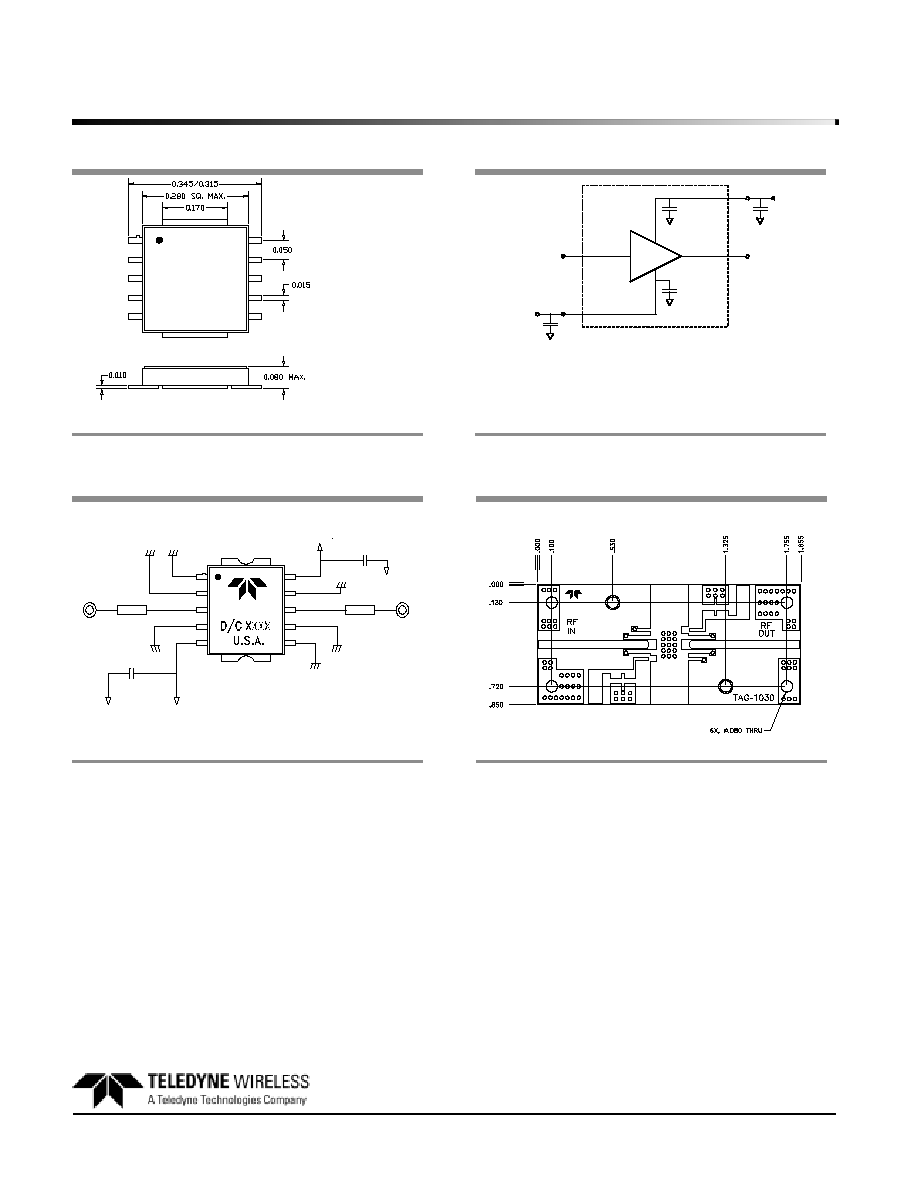
Package Outline
Package Outline
Package Outline
Package Outline
Package Outline
Evaluation Circuit
Evaluation Circuit
Evaluation Circuit
Evaluation Circuit
Evaluation Circuit
Evaluation Board
Evaluation Board
Evaluation Board
Evaluation Board
Evaluation Board
GaAs
MMIC
PACKAGED
AMPLIFIER
470 pF
470 pF
RF Output
RF Input
Input
V
d
V
g
(50 ohms)
(50 ohms)
Bypass
(1
µF Typical)
3
5
8
10
Bypass
(1
µF Typical)
External Components Required:
Bypass Capacitors: 1
µ F, typical
50 Ohm microsrtip interface
Tolerance: .XXX
± 0.005
PIN 1
PIN 6
3
5
8
10
TAG-1030
Vdd
V
6
GND
GND
GND
GND
50 OHM
LINE
50 OHM
LINE
RF
OUT
GND
GND
1.0
µf
GND
RF
IN
1.0
µf
C1
C2
1
2
3
4
5
10
9
8
7
6
GND
Teledyne reserves the right to make changes without further notice to any specification herein. "Typical" parameters can and do vary.
N o t e s
N o t e s
N o t e s
N o t e s
N o t e s
1.
Dual bias supply required.
2.
DC supply sequencing or protection circuitry not included. See Amplifier Biasing Procedure
3.
A 360 pF DC supply line decoupling capacitor is included on both V
d
and V
g
lines. (See typical biasing configuration shown above).
4.
The last fixture or circuit should incorporate additional bypass capacity (25ufd) on the drain and gate bias terminals to prevent oscillations
caused by feedback signals.
5.
Supply (drain and gate) wire/leads should be as short as possible.
6.
Close placement of external components to the power amplifier is essential for stability purposes.
7.
TET recommends the unit be soldered to DC and RF ground for best results.
8.
Pin numbers indicated on outline drawing are for user information only. Units are not labeled with pin numbers.
9.
MASK drawing for circuit board available on the Teledyne Wireless website at www.teledynewireless.com.