 | –≠–ª–µ–∫—Ç—Ä–æ–Ω–Ω—ã–π –∫–æ–º–ø–æ–Ω–µ–Ω—Ç: TC1301 | –°–∫–∞—á–∞—Ç—å:  PDF PDF  ZIP ZIP |
TC1301
REV.2_04/12/2004
TRANSCOM, INC., 90 Dasoong 7
th
Road, Tainan Science-Based Industrial Park, Hsin-She Shiang, Tainan County, Taiwan, R.O.C.
Web-Site: www.transcominc.com.tw
Phone: 886-6-5050086
Fax: 886-6-5051602
P 1 / 6
Low Noise and Medium Power GaAs FETs
FEATURES
∑
Low Noise Figure:
NF = 0.8 dB Typical at 12 GHz
∑
High Associated Gain:
Ga = 10 dB Typical at 12 GHz
∑
High Dynamic Range:
1 dB Compression Power P
-1
= 24 dBm at 12 GHz
∑
Breakdown Voltage:
BV
DGO
9 V
∑
Lg = 0.25
µ
m, Wg = 600
µ
m
∑
All-Gold Metallization for High Reliability
∑
100 % DC Tested
DESCRIPTION
The TC1301 is a GaAs Pseudomorphic High Electron Mobility Transistor (PHEMT) chip, which has very
low noise figure, high associated gain and high dynamic range. The device can be used in circuits up to 40
GHz and suitable for low noise and medium power amplifier applications including a wide range of
commercial and military applications. All devices are 100% DC tested to assure consistent quality. All bond
pads are gold plated for either thermo-compression or thermo-sonic wire bonding.
ELECTRICAL SPECIFICATIONS (T
A
=25
∞
∞
∞
∞
C)
Symbol CONDITIONS
MIN TYP MAX
UNIT
NF
Noise Figure at V
DS
= 4 V, I
DS
= 50 mA,
f = 12GHz
0.8
1.0
dB
G
a
Associated Gain at V
DS
= 4 V, I
DS
= 50 mA, f = 12GHz
9 10
dB
P
1dB
Output Power at 1dB Gain Compression Point , f = 12GHz
V
DS
= 6 V, I
DS
= 80 mA
24
dBm
G
L
Linear Power Gain, f = 12GHz
V
DS
= 6 V, I
DS
= 80 mA
10
11
dB
I
DSS
Saturated Drain-Source Current at V
DS
= 2 V, V
GS
= 0 V
180
mA
g
m
Transconductance at V
DS
= 2 V, V
GS
= 0 V
200
mS
V
P
Pinch-off Voltage at V
DS
= 2 V, I
D
= 1.2 mA
-1.0*
Volts
BV
DGO
Drain-Gate Breakdown Voltage at I
DGO
=0.3 mA
9 12
Volts
R
th
Thermal
Resistance
22
∞
C/W
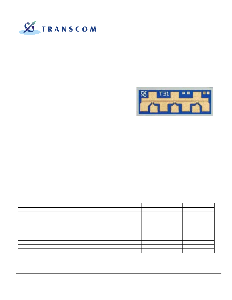
PHOTO ENLARGEMENT
* For the tight control of the pinch-off voltage range, we divide TC1301 into 3 model numbers to fit customer design requirement
(1)TC1301P0710 : Vp = -0.7V to -1.0V (2)TC1301P0811 : Vp = -0.8V to -1.1V (3)TC1301P0912 : Vp = -0.9V to -1.2V
If required, customer can specify the requirement in purchasing document. For special Vp requirement, please contact factory for
details.
TC1301
REV.2_04/12/2004
TRANSCOM, INC., 90 Dasoong 7
th
Road, Tainan Science-Based Industrial Park, Hsin-She Shiang, Tainan County, Taiwan, R.O.C.
Web-Site: www.transcominc.com.tw
Phone: 886-6-5050086
Fax: 886-6-5051602
P 2 / 6
S
G
S
G
S
G
S
D
D
D
760±±±± 12
290±±±± 12
ABSOLUTE MAXIMUM RATINGS (T
A
=25
∞
∞
∞
∞
C)
Symbol Parameter
Rating
V
DS
Drain-Source
Voltage
7.0
V
V
GS
Gate-Source Voltage
-3.0 V
I
DS
Drain
Current
I
DSS
I
GS
Gate
Current
600
µ
A
P
in
RF Input Power, CW
20 dBm
P
T
Continuous Dissipation
800 mW
T
CH
Channel Temperature
175
∞
C
T
STG
Storage Temperature
- 65
∞
C
to +175
∞
C
TYPICAL NOISE PARAMETERS (T
A
=25
∞
∞
∞
∞
C)
V
DS
= 4 V, I
DS
= 50 mA
opt
Frequency NF
opt
G
A
MAG ANG
Rn/50
2
0.36 19.7 0.88 15 0.28
4
0.48 16.6 0.74 39 0.18
6
0.59 14.3 0.62 64 0.15
8
0.70 12.7 0.55 92 0.12
10 0.78
11.7
0.50
120
0.09
12
0.85 10.9 0.49 148
0.06
14
0.98 10.4 0.50 174
0.04
16 1.12 9.8 0.51
-162
0.04
18 1.27 9.0 0.54
-141
0.07
CHIP DIMENSIONS
Units: Micrometers
Gate Pad: 75 x 70
Chip Thickness: 100
Drain Pad: 80 x 70
Source Pad: 75 x 80
TC1301
REV.2_04/12/2004
TRANSCOM, INC., 90 Dasoong 7
th
Road, Tainan Science-Based Industrial Park, Hsin-She Shiang, Tainan County, Taiwan, R.O.C.
Web-Site: www.transcominc.com.tw
Phone: 886-6-5050086
Fax: 886-6-5051602
P 3 / 6
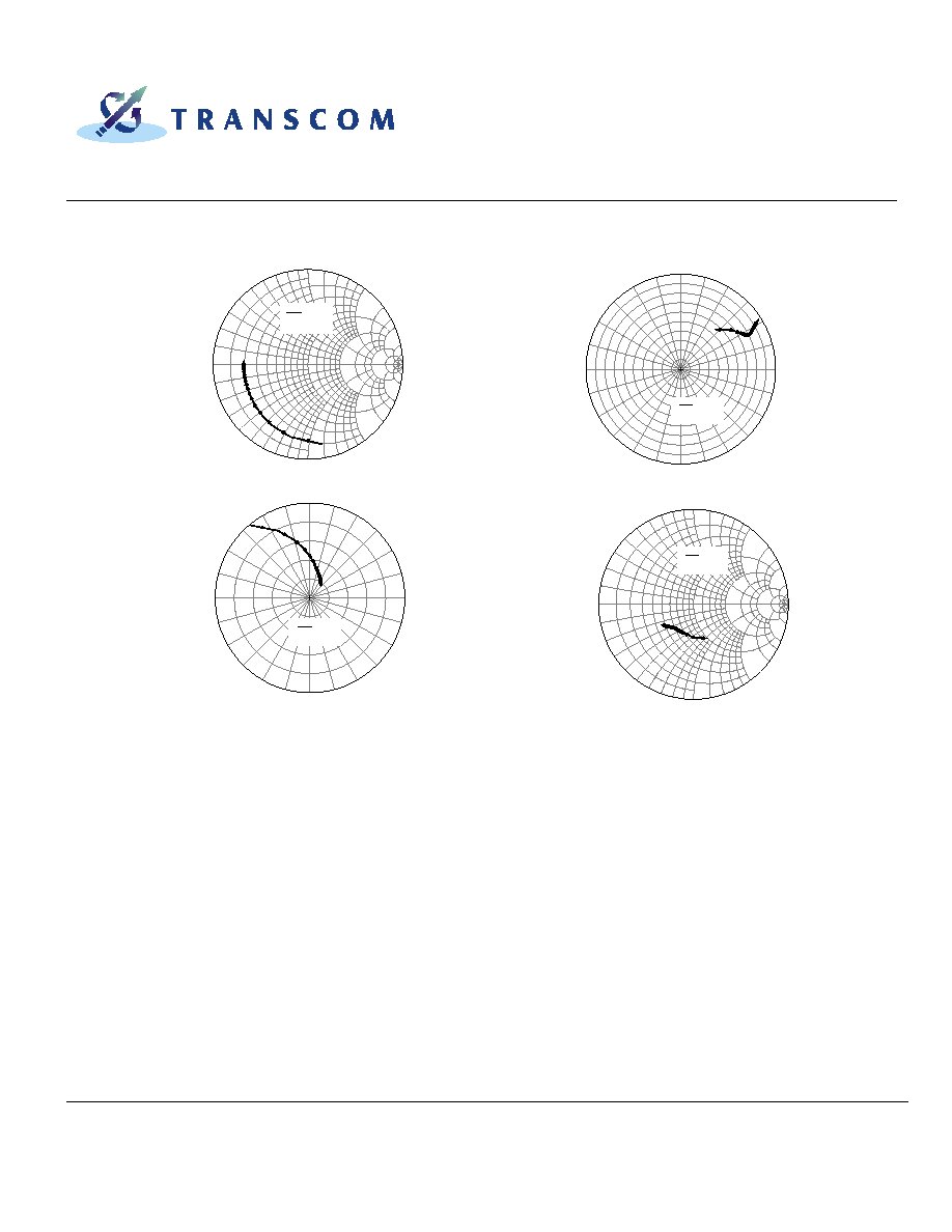
TYPICAL SCATTERING PARAMETERS (T
A
=25
∞
∞
∞
∞
C)
V
DS
= 4 V, I
DS
= 50 mA
FREQUENCY
S11
S21
S12
S22
(GHz)
MAG ANG MAG ANG MAG ANG MAG ANG
2
0.8504 -80.07 9.9111 129.43 0.0557 48.67 0.3868 -68.29
3 0.7843
-103.76
7.8038
115.14
0.0659
38.99
0.3487
-88.15
4
0.7445 -120.17 6.3123
105.04 0.0713
33.48
0.3277 -101.61
5 0.7206
-132.00
5.2595
97.31
0.0745
30.31
0.3178
-111.02
6 0.7058
-140.93
4.4944
91.01
0.0767
28.54
0.3147
-117.84
7
0.6961 -147.93 3.9201
85.60 0.0785
27.63
0.3159 -122.98
8
0.6897 -153.62 3.4764
80.80 0.0800
27.27
0.3198 -127.02
9
0.6853 -158.39 3.1248
76.43 0.0814
27.29
0.3256 -130.30
10
0.6822 -162.46 2.8405
72.38 0.0828
27.56
0.3327 -133.08
11
0.6800 -166.03 2.6065
68.56 0.0843
28.01
0.3406 -135.50
12
0.6785 -169.21 2.4110
64.93 0.0858
28.56
0.3490 -137.67
13
0.6776 -172.07 2.2456
61.46 0.0875
29.19
0.3577 -139.65
14
0.6769 -174.69 2.1042
58.11 0.0892
29.86
0.3667 -141.49
15 0.6766
-177.11
1.9821
54.87
0.0910
30.55
0.3756
-143.23
16
0.6765 -179.36 1.8759
51.72 0.0928
31.23
0.3845 -144.89
17 0.6766
178.52
1.7827
48.65
0.0948
31.89
0.3933
-146.47
18 0.6768
176.52
1.7005
45.65
0.0969
32.53
0.4020
-148.00
∑
The data does not include gate, drain and source bond wires.
0
1.
0
1.
0
-
1.0
1
0.0
10.0
-10.0
5.
0
5.
0
-5.0
2.
0
2.
0
-
2.0
3.
0
3.
0
-3.0
4.
0
4.
0
-4.0
0.
2
0.
2
-0.2
0.
4
0.
4
-
0.4
0.
6
0.
6
-
0.6
0.
8
0.
8
-
0.8
Swp Max
18GHz
Swp Min
2GHz
S11
0
15
30
45
60
75
90
10
5
12
0
13
5
15
0
165
-180
-165
-150
-
135
-
120
-
105
-9
0
-7
5
-6
0
-4
5
-3
0
-15
Swp Max
18 GHz
Swp Min
2 GHz
Mag Max
0.1
0.01
Per Div
S12
0
15
30
45
60
75
90
10
5
12
0
13
5
15
0
165
-180
-16
5
-15
0
-13
5
-12
0
-10
5
-9
0
-7
5
-6
0
-4
5
-3
0
-15
Swp Max
18 GHz
Swp Min
2 GHz
Mag Max
10
2
Per Div
S21
0
1.0
1.0
-1.
0
10.
010.
0
-10.0
5.0
5.0
-5.
0
2.0
2.0
-2.
0
3.0
3.0
-3.
0
4.0
4.0
-4.
0
0.2
0.2
-0.
2
0.4
0.4
-0.
4
0.6
0.6
-0.
6
0.8
0.8
-0.
8
Swp Max
18GHz
Swp Min
2GHz
S22
TC1301
REV.2_04/12/2004
TRANSCOM, INC., 90 Dasoong 7
th
Road, Tainan Science-Based Industrial Park, Hsin-She Shiang, Tainan County, Taiwan, R.O.C.
Web-Site: www.transcominc.com.tw
Phone: 886-6-5050086
Fax: 886-6-5051602
P 4 / 6
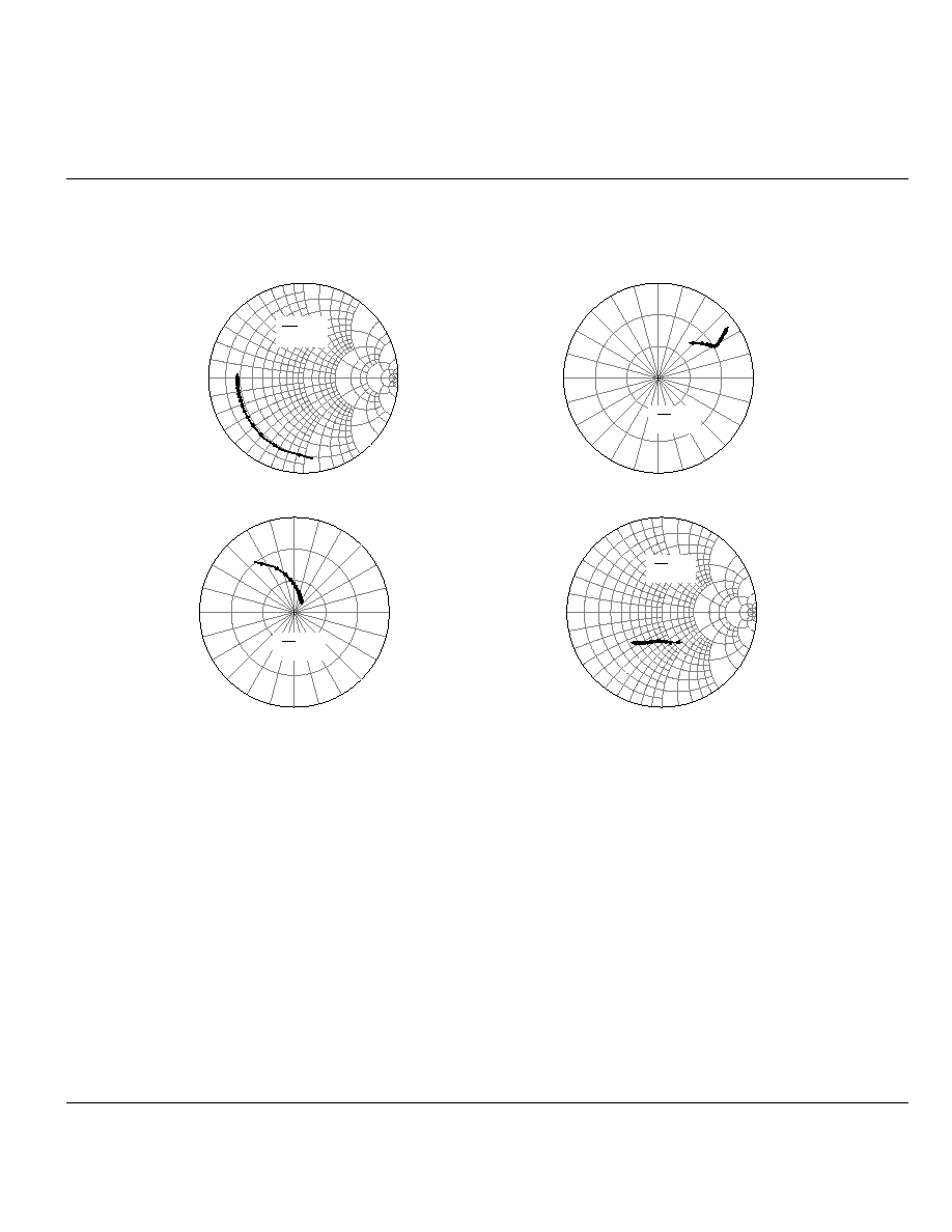
TYPICAL SCATTERING PARAMETERS (T
A
=25
∞
∞
∞
∞
C)
V
DS
= 6 V, I
DS
= 80 mA
FREQUENCY
S11
S21
S12
S22
(GHz)
MAG ANG MAG ANG MAG ANG MAG ANG
2
0.8511 -83.76
10.1160
128.27
0.0446 48.15
0.3787 -56.54
3
0.7902
-107.47 7.8891
114.27
0.0523 39.06
0.3349 -72.15
4
0.7549
-123.54 6.3492
104.51
0.0564 34.17
0.3133 -82.94
5
0.7342
-134.97 5.2766 97.09
0.0590 31.58
0.3059 -90.91
6
0.7214
-143.52 4.5034 91.05
0.0609 30.31
0.3072 -97.18
7 0.7133
-150.20
3.9260
85.88
0.0626
29.84
0.3138
-102.35
8 0.7078
-155.61
3.4814
81.28
0.0641
29.86
0.3237
-106.81
9 0.7041
-160.12
3.1301
77.07
0.0655
30.19
0.3356
-110.76
10 0.7015
-163.98
2.8465
73.16
0.0671
30.73
0.3485
-114.34
11 0.6998
-167.36
2.6134
69.46
0.0686
31.38
0.3620
-117.64
12 0.6986
-170.36
2.4188
65.92
0.0703
32.10
0.3757
-120.71
13 0.6978
-173.08
2.2542
62.52
0.0720
32.85
0.3893
-123.59
14 0.6973
-175.55
2.1134
59.23
0.0738
33.60
0.4027
-126.31
15 0.6971
-177.85
1.9919
56.03
0.0756
34.33
0.4157
-128.89
16 0.6971
-179.98
1.8860
52.90
0.0775
35.03
0.4283
-131.35
17 0.6973
178.01
1.7930
49.83
0.0795
35.70
0.4404
-133.69
18
0.6976 176.11 1.7109 46.82 0.0816 36.32
0.4520 -135.92
∑
The data does not include gate, drain and source bond wires.
0
1.
0
1.
0
-
1.0
1
0.0
10.0
-10.0
5.
0
5.
0
-5.0
2.
0
2.
0
-
2.0
3.
0
3.
0
-3.0
4.
0
4.
0
-4.0
0.
2
0.
2
-0.2
0.
4
0.
4
-
0.4
0.
6
0.
6
-
0.6
0.
8
0.
8
-
0.8
Swp Max
18GHz
Swp Min
2GHz
S11
0
15
30
45
60
75
90
10
5
12
0
13
5
15
0
165
-180
-165
-150
-
135
-
120
-
105
-9
0
-7
5
-6
0
-4
5
-3
0
-15
Swp Max
18 GHz
Swp Min
2 GHz
Mag Max
0.09
0.03
Per Div
S12
0
15
30
45
60
75
90
10
5
12
0
13
5
15
0
165
-180
-165
-1
50
-1
35
-1
20
-1
05
-9
0
-7
5
-6
0
-4
5
-3
0
-15
Swp Max
18 GHz
Swp Min
2 GHz
Mag Max
15
5
Per Div
S21
0
1.0
1.0
-1.
0
10.
010.
0
-10.0
5.0
5.0
-5.
0
2.0
2.0
-2.
0
3.0
3.0
-3.
0
4.0
4.0
-4.
0
0.2
0.2
-0.
2
0.4
0.4
-0.
4
0.6
0.6
-0.
6
0.8
0.8
-0.
8
Swp Max
18GHz
Swp Min
2GHz
S22
TC1301
REV.2_04/12/2004
TRANSCOM, INC., 90 Dasoong 7
th
Road, Tainan Science-Based Industrial Park, Hsin-She Shiang, Tainan County, Taiwan, R.O.C.
Web-Site: www.transcominc.com.tw
Phone: 886-6-5050086
Fax: 886-6-5051602
P 5 / 6
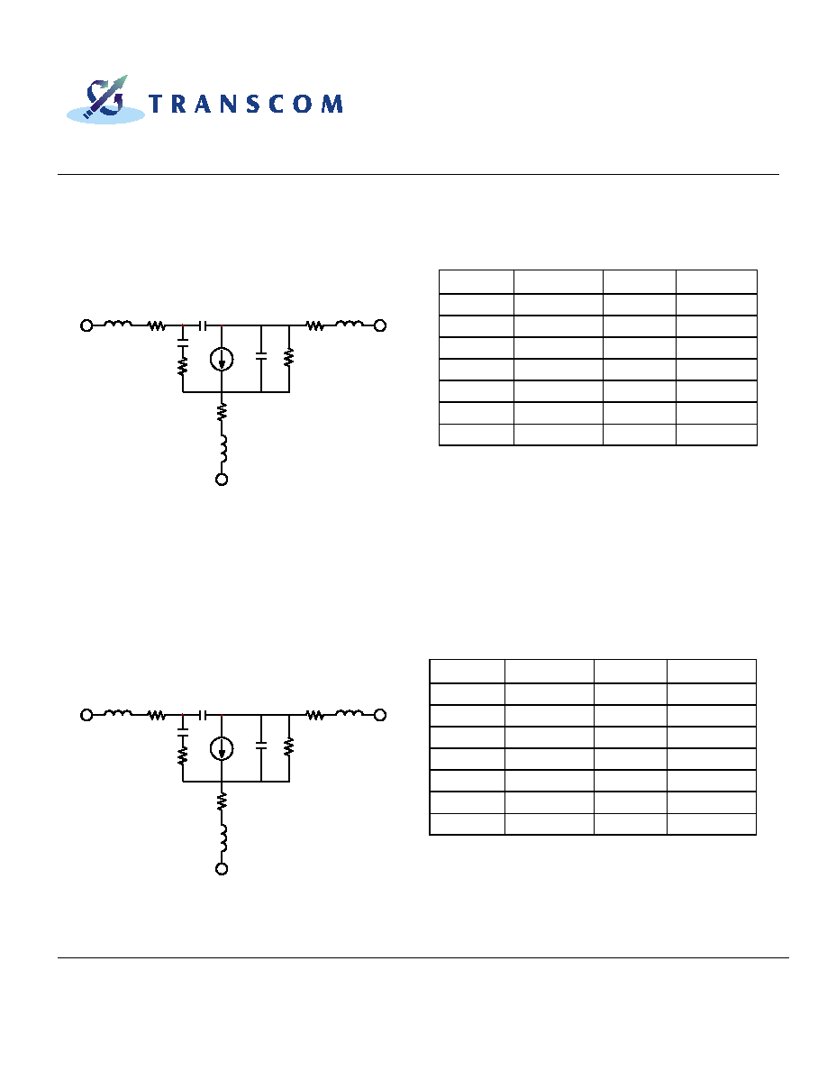
SMALL SIGNAL MODEL, V
DS
= 4 V, I
DS
= 50 mA
Cgs
Cgd
Cds
Rg
Rd
Rds
Ri
Rs
Gm
T
Lg
Ld
Ls
PARAMETERS
Parameters
Parameters
Lg
0.057 nH
Rs
1.66 Ohm
Rg
2.08 Ohm Ls
0.019 nH
Cgs
0.959 pF
Cds
0.167 pF
Ri
5.78 Ohm Rds
93.2 Ohm
Cgd
0.074 pF
Rd
1.358 Ohm
Gm
284.0 mS Ld
0.038 nH
T
5.54 psec
SMALL SIGNAL MODEL, V
DS
= 6 V, I
DS
= 80 mA
Cgs
Cgd
Cds
Rg
Rd
Rds
Ri
Rs
Gm
T
Lg
Ld
Ls
PARAMETERS
Parameters
Parameters
Lg
0.056 nH
Rs
1.808 Ohm
Rg
1.954 Ohm Ls
0.016 nH
Cgs
1.33 pF
Cds
0.185 pF
Ri
5.58 Ohm Rds
90.1 Ohm
Cgd
0.052 pF
Rd
1.422 Ohm
Gm
315 mS Ld
0.036 nH
T
5.63 psec
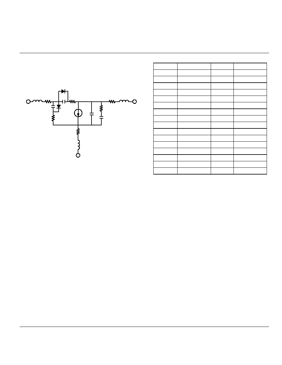
SCHEMATIC
SCHEMATIC
TC1301
REV.2_04/12/2004
TRANSCOM, INC., 90 Dasoong 7
th
Road, Tainan Science-Based Industrial Park, Hsin-She Shiang, Tainan County, Taiwan, R.O.C.
Web-Site: www.transcominc.com.tw
Phone: 886-6-5050086
Fax: 886-6-5051602
P 6 / 6
LARGE SIGNAL MODEL, V
DS
= 6 V, I
DS
=80 mA
TOM2 MODEL PARAMETERS
Parameters
Parameters
VTO
-0.43283 V
VMAX
0.5 V
ALPHA
9.54
CGD
0.0554 pF
BETA
0.49
CGS
6.018 pF
GAMMA
0.0416
CDS
0.1599 pF
DELTA
0.3091
RIS
5.755 Ohm
Q
0.84
RID
0.001 Ohm
NG
0.1
VBR
9 V
ND
0.01
RDB
94.333 Ohm
TAU
5.558 ps
CBS
0.0463 pF
RG
2.0833 Ohm TNOM
25
∞
C
RD
1.358 Ohm LS
0.01893 nH
RS
1.662 Ohm LG
0.0576 nH
IS
1E-11 mA
LD
0.038 nH
N
1
AFAC
1
VBI
1 V
NFING
1
VDELTA
0.2 V
CHIP HANDLING
DIE ATTACHMENT: Conductive epoxy or eutectic die attach is recommended. Eutectic die attach can be
accomplished with Au-Sn (80%Au-20%Sn) perform at stage temperature: 290
∞
C
±
5
∞
C; Handling Tool:
Tweezers; Time: less than 1min.
WIRE BONDING: The recommended wire bond method is thermocompression bonding with 0.7 to 1.0 mil
(0.018 to 0.025 mm) gold wire. Stage temperature: 220
∞
C to 250
∞
C; Bond Tip Temperature: 150
∞
C; Bond Force:
20 to 30 gms depending on size of wire and Bond Tip Temperature.
HANDLING PRECAUTIONS: The user must operate in a clean, dry environment. Care should be exercised
during handling avoid damage to the devices. Electrostatic Discharge (ESD) precautions should be observed at
all stages of storage, handling, assembly, and testing. The static discharge must be less than 300V.
Cgs
Cgd
Cds
Rg
Rd
Rdb
Ris
Rs
Id
Lg
Ld
Ls
Cbs
Rid
SCHEMATIC