 | –≠–ª–µ–∫—Ç—Ä–æ–Ω–Ω—ã–π –∫–æ–º–ø–æ–Ω–µ–Ω—Ç: TC2411 | –°–∫–∞—á–∞—Ç—å:  PDF PDF  ZIP ZIP |
Datasheet (Advance Information)
TC2411
14-Bit,
1
GSPS
Digital-to-Analog Converter
with Standby Mode of Operation
1
Copyright 2004 TelASIC Communications, Inc. All rights reserved. www.telasic.com
Tel:
310.955.3838
.
Specifications subject to change without notice.
The TC2411 is a 14-bit, 1 GSPS digital-to-analog
converter that delivers exceptional high-frequency
performance. The TC2411 is designed to support
single or multiple transmit IF signals up to 500 MHz
and to deliver superior dynamic range at a sampling
rate up to a guaranteed 1 GSPS. A power down
feature has been incorporated into the TC2411
which allows the part to be placed into a Standby
Mode of operation.
∑ High
resolution
∑ High
Clock
rate
∑ Standby Mode for lower power dissipation
Description
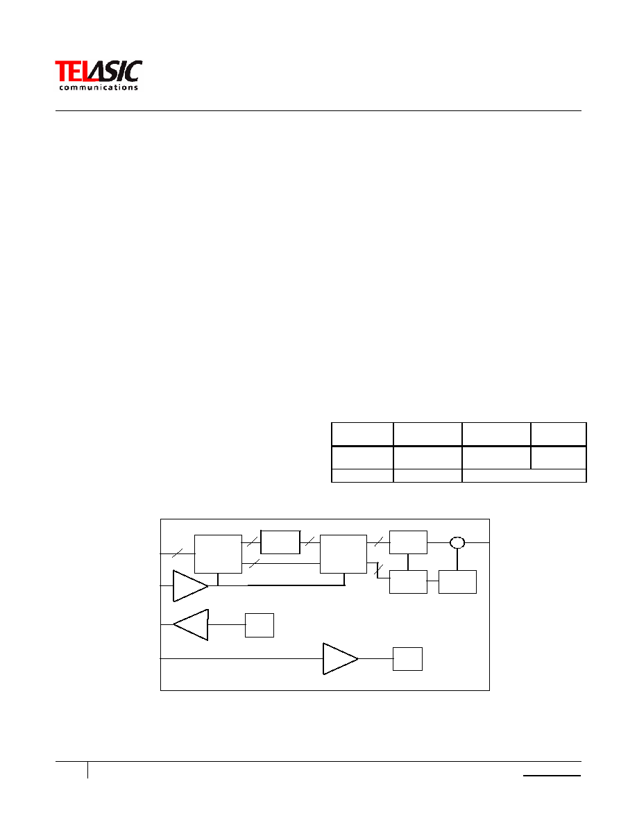
As shown in the functional block diagram below, the
TC2411 features a 5-Bit Unary + 9-Bit Binary R2R
architecture. 14-bit straight binary data can be input
to the DAC at a sample rate of up to 1 GSPS. The
DAC provides low-noise and low-spurious
performance with digital IF input signals across the
first Nyquist band.
The highly linear analog output produced by the
TC2411 may be filtered externally to reject the signal
image, and is suitable for single-stage upconversion
applications.
Applications
The TC2411's high sample rate makes it ideal for
the following applications:
∑ Signal
generation
∑ Direct digital synthesis (DDS)
∑ Test and measurement
∑ Software
radio
∑ Single- and multi-carrier transceivers
∑ Radar (Including Burst mode capability)
Technical Features
∑ Signal-Noise
Ratio.................74dBc
@126MHz
∑ Signal Input...............1000MSPS, 14bits LVDS
∑ Spur Free Dynamic Range......75dBc @126MHz
∑ Clock Input Drive.. 0 to +13dBm, 25 differential
∑ Full Scale Output...........-2dBm, 50 differential
∑ Voltage Reference.........2.5V Bandgap On-Chip
∑ Power Dissipation .................................1.8W
∑ Technology ...................0.5 µm SiGe BiCMOS
∑ Packaging......96
ball,
Pb-free, Cavity-down BGA
Ordering Information
PART
NUMBER
TEMP RANGE
(∞C)
PACKAGE
CLOCK
SPEED
TC2411-IB -40∞C
to
+85∞C
96 ball Pb-free
BGA
1000 MHz
TC2411-KIT +25C
Evaluation
Kit
Digital
Input
Clock In
2.5V
Ref Out
2.5V
Ref In
Analog
Output
Buffer
+
Register
5 MSB
Decode
Register
Unary
Binary
R-2R
Ladder
Amp
Amp
Ref
Cell
Band
Gap
Buf
14
5
31
31
9
9
Figure 1: TC2411 Functional Block Diagram
Datasheet (Advance Information)
TC2411
2
MKDSTC2411 Rev-
Absolute Maximum Ratings
(Electrical performance is not guaranteed at absolute maximum ratings. Exposure to absolute
maximum ratings for an extended period of time may impair the useful life of the product)
Parameter Max
Unit
Electrical
+5.0V Supply Voltage AVCC, DVDD
+5.5
V
+3.3V Supply Voltage DVCC
+3.6
V
-5.0V Supply Voltage AVEE, DVEE
-5.5
V
Clock Input Voltage
+4.0
Vpp
Environmental
Operating Temp Range
-40 to +85
o
C
Storage Temp Range
-65 to +150
o
C
Maximum Junction Temperature
+110
o
C
Reflow Soldering Peak Temperature
+260
o
C
TC2411 Electrical Specifications
(AVEE, DVEE = -5V; AVCC, DVDD = +5V; DVCC = +3.3V; IOUT = 20 mA, -40
o
C to +85∞C ambient, unless otherwise noted)
DC SPECIFICATIONS
CONDITION
MIN
TYP
MAX
UNITS
Supply Voltages
AVCC, DVDD
4.75
5.0
5.25
V
DVCC
3.13
3.3
3.46
V
AVEE
-5.25
-5.0
-4.75
V
DVEE
-5.25
-5.0
-4.75
V
Normal Mode
AVCC + DVDD + DVCC Current
30
mA
AVEE + DVEE Current
330
mA
Power Consumption
1.8
W
Reference Voltage info
Vout_REF
2.5
V
Reference Output Load Regulation
0 < Isource < Imax
mV
Resolution
14
Bits
Standby
Mode
AVCC + DVDD + DVCC Current
40
mA
AVEE + DVEE Current
140
mA
Power Consumption
850
mW
Datasheet (Advance Information)
TC2411
3
MKDSTC2411 Rev-
TC2411 Electrical Specifications continued
(AVEE, DVEE = -5V; AVCC, DVDD = +5V; DVCC = +3.3V; IOUT = 20 mA, -40
o
C to +85∞C ambient, unless otherwise noted)
DIGITAL SPECIFICATIONS
CONDITION MIN
TYP
MAX
UNITS
Logic Inputs (N1- N14, P1 ≠ P14)
Compatibility
LVDS
Input Impedance
100
ohms
Common Mode Voltage (VCM)
+1.2
V
Differential Input High Level
VCM = +1.2V
+100
mV
Differential Input Low Level
VCM = +1.2V
-100
mV
Data Coding
Binary
Switching characteristics
Setup Time
130
ps
Hold Time
440
ps
Propagation Delay Time
400
ps
Data Rise Time
10% to 90 %
220
ps
Data Fall Time
90% to 10 %
230
ps
Reset (RST)
High Level
3.3
Volts
Low Level
0
Volts
Pulse Width
2.5
ns
Pulse Repetition Rate
DC
200
MHz
Propagation Delay
3
Clock
cycles
Standby Mode (SLP, SLN)
Single Ended Drive
Low Level
0
Volts
High Level
3.3
Volts
Differential drive (External100
)
Low Level
1.0
Volts
High Level
1.4
Volts
ANALOG SPECIFICATIONS
CONDITION
MIN
TYP
MAX
UNITS
DAC Clock (CLKP, CLKN)
Maximum Conversion Rate
Guaranteed
1000
MSPS
Differential Input Voltage
1.5
Vpp
Common-mode Input Voltage
-3.1
V
Differential Input Resistance
25
ohms
Analog Output (VOP, VON)
Full Scale Output Voltage
20 mA Differential
Output Current
0.480 Vp-p
Differential Output Resistance
50
ohms
Datasheet (Advance Information)
TC2411
4
MKDSTC2411 Rev-
DYNAMIC SPECIFICATIONS
CONDITION
MIN
TYP
MAX
UNITS
DAC Output vs Frequency @ -0.5 dBFS
f
out
= 33 MHz
-3
dBm
f
out
= 126 MHz
-3
dBm
f
out
= 251 MHz
-5
dBm
f
out
= 376 MHz
-8
dBm
f
out
= 490 MHz
-9
dBm
Noise Spectral Density @ -0.5 dBFS
f
out
= 33 MHz
-166
dBm/Hz
f
out
= 126 MHz
-164
dBm/Hz
f
out
= 251 MHz
-161
dBm/Hz
f
out
= 376 MHz
-161
dBm/Hz
f
out
= 490 MHz
-160
dBm/Hz
SFDR vs Frequency @ -0.5 dBFS
f
out
= 33 MHz
-78
dBc
f
out
= 126 MHz
-75
dBc
f
out
= 251 MHz
-70
dBc
f
out
= 376 MHz
-65
dBc
f
out
= 490 MHz
-60
dBc
IMD
IF = 135 MHz, 145 MHz
2 Tones @ -6.5 dBFS
-82
dBc
IF = 110 MHz, 120 MHz, 130 MHz, 140 MHz
4 Tones @ -12.5 dBFS
-82
dBc
ACPR (EDGE)
IF = 260 MHz
1 Tone @ -3.5 dBFS
-95
dBc
IF = 230 MHz, 240 MHz, 260 MHz, 270 MHz
4 Tones @ -15.5 dBFS
-88
dBc
ACPR (WCDMA)
IF = 260 MHz
1 Tone @ -10.5 dBFS
-75
dBc
IF = 230 MHz, 240 MHz, 260 MHz, 270 MHz
4 Tones @ -17.5 dBFS
-76
dBc
Analog Output Response
Output Settling Time
pS
Output Rise Time (10 - 90%)
220
pS
Output Fall Time (90 ≠ 10%)
230
pS
Glitch Energy
-FS to +FS transition
FS = Full-Scale
0.5
ps-V
+FS to -FS transition
0.1
ps-V
-MS to +MS transition
MS = Mid-Scale
0.4
ps-V
+MS to -MS transition
0.2
ps-V

Datasheet (Advance Information)
TC2411
5
MKDSTC2411 Rev-
TC2411 Thermal Characteristics
Normal Mode of Operation
JA
(
o
C/W)
Package
JC
(
o
C/W)
0 m/s
2m/s
3m/s
Note
19X19 Cavity-down
BGA 96L
2.72 20.2
18.5
17.5
Results based on FEA simulation
without heat sink.
∑ The DC power of the TC2411 is 1.8 W in normal mode of operation
∑ Maximum Junction Temperature is not to exceed 110
o
C.
∑ There is no need for an external heat sink if maximum ambient temperature is +70
o
C.
∑ An external heat sink is recommended for ambient temperatures in excess of +70
o
C to insure that the
junction temperature does not exceed 110
o
C maximum.
∑ Use of standby mode reduces the average power dissipation proportional to the normal mode / standby
mode duty cycle and allows a higher ambient temperature before a heat sink must be used to insure that
the junction temperature does not exceed 110
o
C maximum.
∑ In the above table,
JA
is presented according to JEDEC JESD 51-2 (natural convection) and 51-6 (forced
convection). Thermal simulation assumes the package is mounted on the test board specified by JEDEC
JESD51-9 (101.6X114.3X1.6 mm, four layers).
Note:
JC
: Thermal resistance from junction to case.
JA
: Thermal resistance from junction to ambient.
Figure 2: Standby Mode Operational Truth Table
Control Signal Normal
Mode Standby
Mode
STDBY_P L
H
STDBY_N H
L
Figure 3: Standby/Normal Mode Timing
STDBY_P
STDBY_N
<5
µ
S
<5
µS
Normal Mode
Standby
Mode
Standby
Mode
Datasheet (Advance Information)
TC2411
6
MKDSTC2411 Rev-
Figure 4:
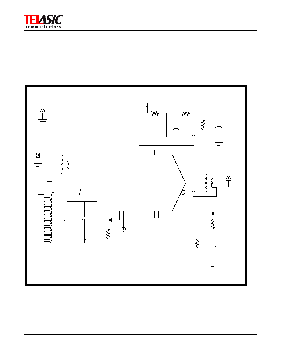
TC2411 Typical Application Circuit
R1
2.0K
1
3
4
2
6
VOP
VON
EXTCAP
Data
CLKP
CLKN
DV
C
C
An
o
d
e
Ca
t
h
o
d
e
DV
C
C
Vo
u
t
_
R
e
f
Vr
e
f
_
R
A
RS
T
Vb
b
SL
P
SL
N
AGND
Analog
Output
AGND
Clk
In
AGND
AGND
AGND
+5VA
R8
110
R7
330
C 7
1000pF
DGND
+5VD2
C 4
1000pF
C 3
0.01uF
-5VA1
T2
T1
J1
J2
J3
D0
D 1
D2
D3
D4
D5
D6
D7
D8
D9
D10
D11
D12
D13
14 pairs
Di
gi
t
a
l
In
p
u
t
TP33
DGND
+5VD2
U1
TC2411
R6
1K
R5
510
R4
560
C 6
1000pF
C5
1000pF
DGND
L1
4
M1
4
M1
A4
B2
B1
D14
C14
G14
F14
D1
N[1:14]
P[1:14]
A3
B3
K1
3
M2
6
4
3
2
1
DV
C
C
A8
Stdby
J3

Datasheet (Advance Information)
TC2411
7
MKDSTC2411 Rev-
Figure 4 (Cont): TC2411 Typical Application Circuit
AGND
G2 (AG
N
D
)
A1
3 (
A
G
N
D)
B13
(
A
G
N
D
)
C1
3
(
A
G
N
D
)
D1
3
(
A
GN
D)
E1
3
(
A
GN
D)
F1
3
(
A
G
N
D)
G1
3 (AG
N
D
)
A1
4 (
A
G
N
D)
B14
(
A
G
N
D
)
E1
4
(
A
GN
D)
B11 (
A
G
N
D
)
F2
(
A
G
N
D
)
E2
(
A
G
N
D)
B9
(
G
N
D
_
T
R
I
M
)
B10
(
G
N
D
_
T
R
I
M
)
DGND
H1
(
G
N
D
)
J1
(
G
N
D
)
H2
(
G
N
D
)
J2
(
G
N
D
)
J1
3
(
G
N
D
)
A1
(
N
C
)
C2
(NC)
A5 (
D
GN
D
)
A6 (
D
GN
D
)
A7 (
D
GN
D
)
A9 (
D
GN
D
)
A1
0 (
D
G
N
D
)
A
11 (
N
C
)
B4
(V
P
1
N
7
_
T
R
)
TP36
TP37
FL8
C19
0.1uF
-5VD1
DGND
FL4
C16
0.1uF
-5VA1
AGND
FL5
FL1
C12
0.1uF
-5VA2
AGND
C13
0.1uF
FL2
C15
0.1uF
-5VD
DGND
FL9
C20
0.1uF
DGND
-5VDT
FL7
C18
0.1uF
+5VD2
DGND
FL3
C14
0.1uF
+5VA
AGND
U2
BNX002
VR1
6.2V
C8
68uF
C9
0.01uF
4
5
6
2
1
3
PS_GND
U3
BNX002
VR2
6.2V
C10
68uF
C11
0.01uF
4
5
6
2
1
3
PS_GND
-5V
+5V
AGND
DGND
1
2
3
4
5
6
7
8
9
J4
PS_GND
Po
wer
-5VPS
+5VPS
J1
4
(
D
V
E
E
)
K1
4 (D
VEE
)
-5VD1
L
1
(
D
V
EE)
L2
(
D
VE
E)
-5VD
K1
(
D
VE
E)
K2
(D
VE
E)
B
5
(
D
V
EE)
B
6
(
D
V
EE)
-5VDT
E1
(
A
V
E
E)
F1
(
A
V
E
E
)
-5VA1
G
1
(
A
V
EE)
A1
2 (
A
VE
E)
B12
(
A
V
E
E
)
-5VA2
H1
3
(
A
V
E
E
)
H1
4
(
A
V
E
E
)
B
7
(
D
V
DD)
B
8
(
D
V
DD)
+5VD2
L13
(
D
VD
D
)
A
2
(A
V
CC)
+5VA
TC2411 Typical Application Circuit Parts List
FIND #
QTY
REFERENCE
DESIGNATOR
TYPE VALUE
TOLERANCE MANUFACTURER / DESCRIPTION
1
4
C4, C5, C6, C7
Capacitor
1000pF
10%
X7R
2
3
C3, C9, C11
Capacitor
0.01uF
10%
X7R
3 2 C8,
C10 Capacitor 68uF 10% Tantalum
4
8
C12, C13, C14,
C15, C16, C18,
C19, C20
Capacitor 0.1uF
10% X7R
5
8
Fl1, Fl2, Fl3,
Fl4, Fl5, Fl7,
Fl8, Fl9
Ferrite Bead
BLM18A
G221SN
Murata
6 1
R1
Resistor 2.0K 5%
7 1
R4
Resistor 560
1%
8 1
R5
Resistor 510
1%
9 1
R6
Resistor 1K
2%
10 1
R7
Resistor 330
2%
11 1
R8
Resistor 110
2%
12
1
T1
Transformer
TX-2-5-1
2%
Mini-Circuits, 2:1 impedance ratio
13
1 T2
Transformer
ADT1-
1WT
2%
Mini-Circuits, 1:1 impedance ratio
14
1
U1
DAC
TC2411
TelASIC, 14 Bit, 1GHz DAC
15
2
U2, U3
EMI Filter
BNX002
Murata
16
2
VR1, VR2
Zener
6.2V
1 Watt

Datasheet (Advance Information)
TC2411
8
MKDSTC2411 Rev-
TC2411 Performance Characteristics
Figure 5: SFDR vs. Frequency @ -0.5 dBFS*
SFDR vs. Frequency
-90
-80
-70
-60
-50
-40
-30
-20
-10
0
0
50
100
150
200
250
300
350
400
450
500
Frequency (MHz)
S
F
DR
(
d
Bc
)
* The values in Figure 1 include coax and filter losses in
the setup.
Figure 6: Noise Floor vs. Frequency
Noise Floor vs. Frequency
-167
-166
-165
-164
-163
-162
-161
-160
-159
-158
0
50
100
150
200
250
300
350
400
450
500
Frequency (MHz)
No
is
e
F
l
o
o
r
(
d
Bm
/H
z
Figure 7: Clock Power Level vs. Noise
Noise Floor vs Clock Power
-166
-165
-164
-163
-162
-161
-160
-159
-158
-6
-4
-2
0
2
4
6
8
10
Clock Power (dBm)
N
o
i
s
e
Fl
oor
(
d
B
m
/
H
z
)
Fout = 49 MHz
Fout = 149 MHz
Fout = 249 MHz
Figure 9: Two tone IMD (dBc) vs. Frequency
Intermodulation Distortion vs. Frequency
-90
-80
-70
-60
-50
-40
-30
-20
-10
0
0
50
100
150
200
250
300
350
400
Frequency Center (MHz)
I
n
t
e
r
m
odul
a
t
i
on D
i
s
t
or
t
i
on (
d
B
c
)
Figure 8: DAC Output Level vs. Frequency
DAC Output Level vs Frequency
-9
-8
-7
-6
-5
-4
-3
-2
-1
0
0
50
100
150
200
250
300
350
400
450
500
Frequency (MHz)
DA
C Ou
t
p
u
t
(
d
B
m
)

Datasheet (Advance Information)
TC2411
9
MKDSTC2411 Rev-
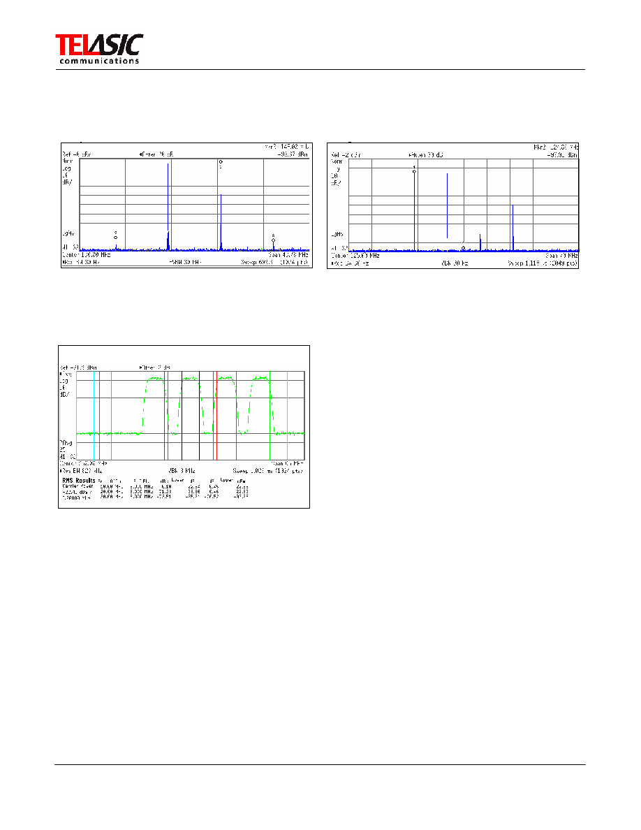
Figure 10: SFDR at 33 MHz (-77 dBc)
Figure 11: SFDR at 126 MHz (-75 dBc)
Figure 12: SFDR at 251 MHz (-72 dBc)
Figure 13: SFDR at 490 MHz (-61 dBc)
Datasheet (Advance Information)
TC2411
10
MKDSTC2411 Rev-
Figure 14: 2-Tone IMD (-82 dBc)*
Figure 15: 4-Tone IMD (-82 dBc)*
Figure 16: ACPR 4-Tone WCDMA (-76 dBc)*
* listed values indicate the actual measured levels, whereas plots shown here are limited by the instrument dynamic range
Datasheet (Advance Information)
TC2411
11
MKDSTC2411 Rev-
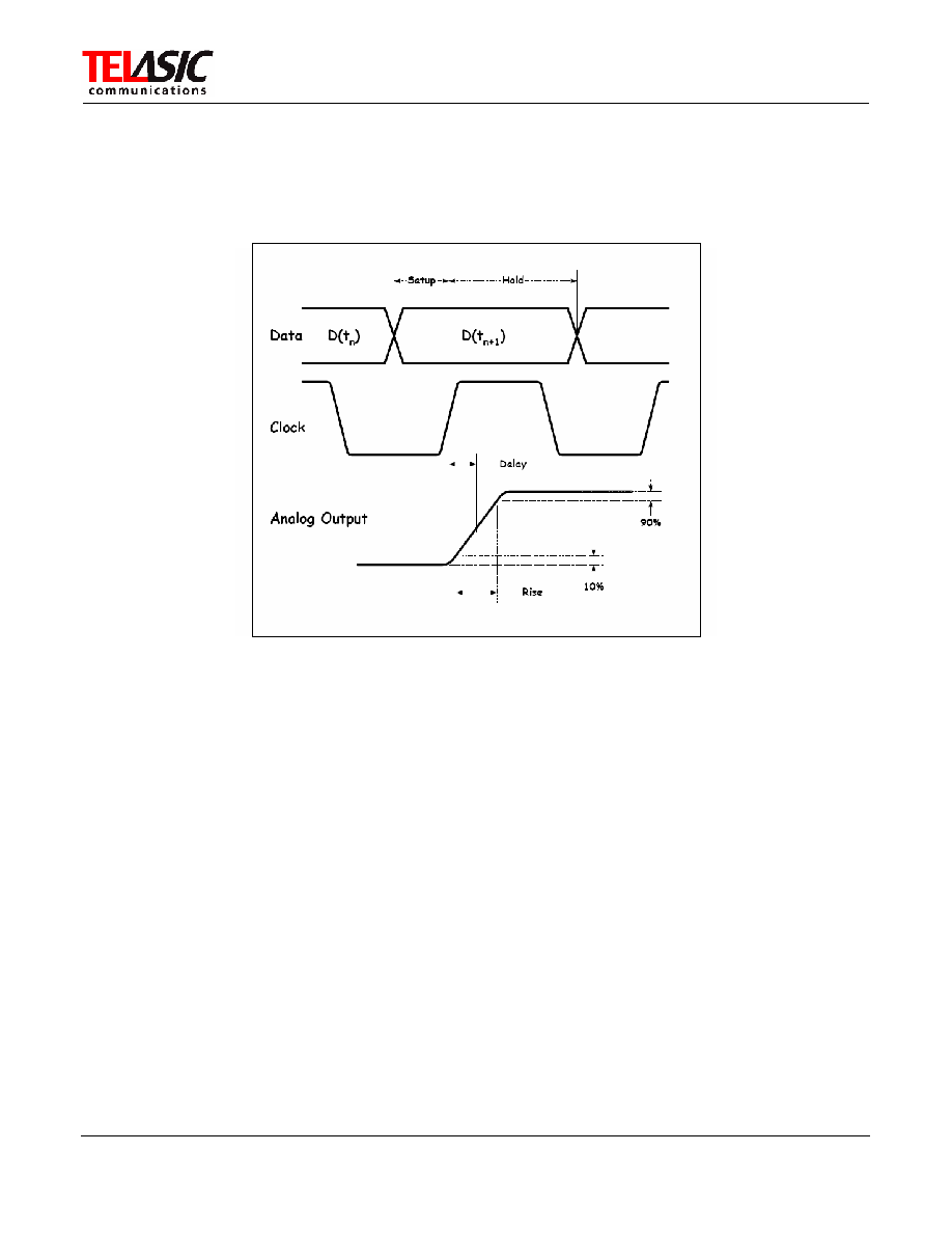
Figure 17: TC2411 Timing Diagram

Datasheet (Advance Information)
TC2411
12
MKDSTC2411 Rev-
Figure 18: TC2411 Pinouts ≠ 96 Ball Cavity-Down BGA Package (Ball Side UP)
AGND
AGND
AGND
AGND
AGND
AGND
AGND
AGND
AGND
AGND
AVEE
AVEE
AVEE
AGND
AGND
AGND
AGND
AVEE
AVEE
AVEE
DGND
DGND
DGND
DGND
DGND
DVEE
DVEE
DVEE
DVEE
DVEE
DVEE
D0P
D13P
D3P
D2P
D4P
D5P
D6P
D7P
D8P
D9P
D10P
D11P
D12P
D1P
D0N
D1N
D2N
D3N
D4N
D5N
D6N
D7N
D8N
D9N
D10N
D11N
D12N
D13N
DVCC
ANODE
AVCC
CATHODE
VREF_
RA
DVDD
VP1N7_
TR
VOUT_
REF
VON
VOP
CLKN
CLKP
AVEE
DVCC
SLP
DVDD
SLN
DNC3
DNC1
DNC2
EXTCAP
DVCC
RST
14
13
12
11
10
9
8
7
6
5
4
3
2
1
A
B
C
D
E
F
G
H
J
K
L
M
N
P
NC
DGND DGND
DGND DGND DGND
AGND
AGND
AGND AGND
DVEE
DVEE
DVDD
VBB
Datasheet (Advance Information)
TC2411
13
MKDSTC2411 Rev-
TC2411 I/O Descriptions
PIN NAME DESCRIPTION
PIN NAME DESCRIPTION
A1 AGND
ANALOG
GND
N1
D13P
DATA INPUT BIT 13 (MSB)
A2
AVCC
+5V REF AMP SUPPLY
N2
D12P
DATA INPUT BIT 12
A3
ANODE
ANODE FOR TEMPERATURE DIODE
N3
D11P
DATA INPUT BIT 11
A4
VBB +2.4V
Bias
N4
D10P
DATA INPUT BIT 10
A5
DGND DIGITAL
GND
N5
D9P
DATA INPUT BIT 9
A6
DGND DIGITAL
GND
N6
D8P
DATA INPUT BIT 8
A7
DGND DIGITAL
GND
N7
D7P
DATA INPUT BIT 7
A8
DVCC
+3.3V SUPPLY FOR ESD
N8
D6P
DATA INPUT BIT 6
A9
DGND DIGITAL
GND
N9
D5P
DATA INPUT BIT 5
A10
DGND DIGITAL
GND
N10
D4P
DATA INPUT BIT 4
A11
NC NO
CONNECT
N11
D3P
DATA INPUT BIT 3
A12
AVNS
-5V ANALOG SUPPLY
N12
D2P
DATA INPUT BIT 2
A13
AGND ANALOG
GND
N13
D1P
DATA INPUT BIT 1
A14
AGND ANALOG
GND
N14
D0P
DATA INPUT BIT 0 (LSB)
B1
VOUT_REF VOLTAGE REFERENCE OUTPUT, +2.5V
P1
D13N
DATA INPUT BIT 13 ≠ COMPLEMENT
(MSB)
B2
VREF_RA
REFAMP INPUT
P2
D12N
DATA INPUT BIT 12 ≠ COMPLEMENT
B3
CATHODE
CATHODE FOR TEMPERATURE DIODE
P3
D11N
DATA INPUT BIT 11 ≠ COMPLEMENT
B4
VP1N7_TR
-1.7V TEST POINT
P4
D10N
DATA INPUT BIT 10 ≠ COMPLEMENT
B5
DVEE -5V
SUPPLY
P5
D9N
DATA INPUT BIT 9 ≠ COMPLEMENT
B6
DVEE -5V
SUPPLY
P6
D8N
DATA INPUT BIT 8 ≠ COMPLEMENT
B7
DVDD
+5V DIGITAL SUPPLY
P7
D7N
DATA INPUT BIT 7 ≠ COMPLEMENT
B8
DVDD
+5V DIGITAL SUPPLY
P8
D6N
DATA INPUT BIT 6 ≠ COMPLEMENT
B9
AGND
ANALOG GND
P9
D5N
DATA INPUT BIT 5 ≠ COMPLEMENT
B10
AGND
ANALOG GND
P10
D4N
DATA INPUT BIT 4 ≠ COMPLEMENT
B11
AGND
ANALOG GND
P11
D3N
DATA INPUT BIT 3 ≠ COMPLEMENT
B12
AVEE
-5V ANALOG SUPPLY
P12
D2N
DATA INPUT BIT 2 ≠ COMPLEMENT
B13
AGND
ANALOG GND
P13
D1N
DATA INPUT BIT 1 ≠ COMPLEMENT
B14
AGND
ANALOG GND
P14
D0N
DATA INPUT BIT 0 ≠ COMPLEMENT
(LSB)
C1
DNC1
DO NOT CONNECT
H1
DGND
DIGITAL GND
C2
AGND
ANALOG GND
H2
DGND DIGITAL
GND
C13
AGND
ANALOG GND
H13
AVEE
-5V ANALOG SUPPLY
C14
VON
DAC ANALOG OUPUT ≠ COMPLEMENT
H14
AVEE
-5V ANALOG SUPPLY
D1
EXTCAP
REF AMP BYPASS CAPACITOR
J1
DGND
DIGITAL GND
D2
DNC2
DO NOT CONNECT
J2
DGND DIGITAL
GND
D13
AGND
ANALOG GND
J13
DGND DIGITAL
GND
D14
VOP DAC
ANALOG
OUPUT
J14
DVEE
-5V DIGITAL SUPPLY
E1
AVEE
-5V ANALOG SUPPLY
K1
DVEE
-5V DIGITAL SUPPLY
E2
AGND
ANALOG GND
K2
DVEE
-5V DIGITAL SUPPLY
E13
AGND
ANALOG GND
K13
DVCC +3.3V
DIGITAL
SUPPLY
E14
AGND
ANALOG GND
K14
DVEE
-5V DIGITAL SUPPLY
F1
AVEE
-5V ANALOG SUPPLY
L1
DVEE
-5V DIGITAL SUPPLY
F2
AGND
ANALOG GND
L2
DVEE
-5V DIGITAL SUPPLY
F13
AGND
ANALOG GND
L13
DVDD
+5V DIGITAL SUPPLY
F14
CLKN
DAC CLOCK INPUT ≠ COMPLEMENT
L14
SLP STANDBY
INPUT
G1
AVEE
-5V ANALOG SUPPLY
M1
RST
RESET/BURST MODE
G2
AGND
ANALOG GND
M2
DVCC
+3.3V SUPPLY FOR ESD
G13
AGND
ANALOG GND
M13
DNC3
DO NOT CONNECT
G14
CLKP
DAC CLOCK INPUT
M14
SLN
STANDBY INPUT - COMPLEMENT

Datasheet (Advance Information)
TC2411
14
MKDSTC2411 Rev-
Application Notes:
A. Power Supply Decoupling
Add power supply decoupling nearby package pins as summarized below:
1. AVEE ≠ bypass each group of pins with 0.1 uF capacitor to AGND.
a. A12,
B12
b. E1, F1, G1
c. H13,
H14
2. DVEE ≠ bypass each group of pins with 0.1 uF capacitor to DGND.
a. K1, K2, L1, L2
b. J14,
K14
c. B5,
B6
3. DVDD ≠ bypass each group of pins with 0.1 uF capacitor to DGND.
a. B7,
B8
b. L13
4. AVCC ≠ bypass pin A2 with 0.1 uF capacitor to AGND.
5. DVCC ≠ bypass pins A8, M2 and K13 with 1000 pF capacitor to DGND.
B. Analog Outputs (VOP, VON)
The TC2411 supplies differential analog DAC outputs at pins VOP and VON. Each pin is internally
terminated with 25 ohms to analog ground, creating an effective 50 ohm differential source. When these
outputs are connected to a single-ended, 50 ohm load through a 1:1 transformer, the resulting full-scale AC
swing is approximately 500 mVpp (20 mA into 25 ohms). Each DAC output may be dc-coupled to a ground-
referenced load.
C. Clock Inputs (CLKP, CLKN)
To achieve excellent phase noise performance, the TC2411 requires a differential clock input with low jitter
characteristics. A 2:1 transformer may be used to convert a single-ended, 50 ohm clock source and provide a
25 ohm, ac-coupled, differential drive into CLKP and CLKN. These inputs are internally biased and
terminated with 12.5 ohms per side.
A very low-phase noise (low jitter) sinewave clock signal should be used for enhanced SNR performance. A
sinewave oscillator featuring at least -130 dBc/Hz phase noise, above 20 KHz from the carrier is
recommended. Best noise performance is achieved with clock sources capable of 1.5 Vpp or greater outputs.
D. LVDS-Compliant Digital Inputs (D0P/N to D13P/N)
The TC2411 offers an LVDS-compliant interface into the 14 bit data inputs. These inputs are differentially
terminated on-chip with 100 ohms. 0000 corresponds to minus full-scale, while 3FFF represents plus full-
scale.
E. Reset/Burst Mode (RST)
The TC2411 offers a burst mode capability whereby the DAC analog output can be asynchronously reset to
the all zeros code (00 0000 0000 0000) irrespective of input data. Under normal operation, the RST pin
should be held high at +3.3V. When a low signal (0V) is applied to RST, the DAC output resets to the all
zeros code (minus full scale). Contact TelASIC sales for further information.

Datasheet (Advance Information)
TC2411
15
MKDSTC2411 Rev-
F. Temperature Diode (ANODE, CATHODE)
The TC2411 provides an on-chip temperature diode which may be used to monitor die temperature. Applying
+5V to the anode pin and measuring the cathode node voltage into a 2K ohm load, the user can convert the
resulting voltage into a temperature. Contact TelASIC sales for further information.
G. External Capacitor for Ref Amp (EXTCAP)
The on-chip reference amplifier requires an external capacitor to maintain excellent phase noise and jitter
characteristics. Attach two capacitors, 0.01 uF and 1000 pF, in parallel between the EXTCAP pin and -5V
analog supply.
H. Ref Amp Input (VREF_RA)
VOUT_REF is an internally generated, +2.5V precision bandgap reference. Tie this output to VREF_RA, the
ref amp input.
I. Standby Mode Function (SLP, SLN)
The TC2411 offers a Standby Mode capability whereby the power dissipation is reduced to 850mW. The
standby function comes in on pins L14 (SLP) and M14 (SLN). Under normal operation both pins are left
floating. This mode may be enabled with either a single-ended drive or a differential drive.
Single-ended drive, M14 (SLN) pin should be left floating and L14 (SLP) pin should be held low at +0.0V for
normal operation, L14 (SLP) pin should be held high at +3.3V (CMOS) for standby mode.
Differential drive level requires external 100 ohm resistor between pins L14 (SLP) and M14 SLN) and uses
standard LVDS, (i.e. low level is 1.0V, high level is 1.4V). For normal mode M14 (SLN) is set low and L14
(SLP) is set high. For sleep mode M14 (SLN) is set high and L14 (SLP) is set low.
J. Do Not Connect Pins
Pins DNC1 (C1), DNC2 (D2), and DNC3 (M13) should be left floating. Connecting these pins to ground or to
either supply voltage will alter device performance and may damage the part.
Datasheet (Advance Information)
TC2411
16
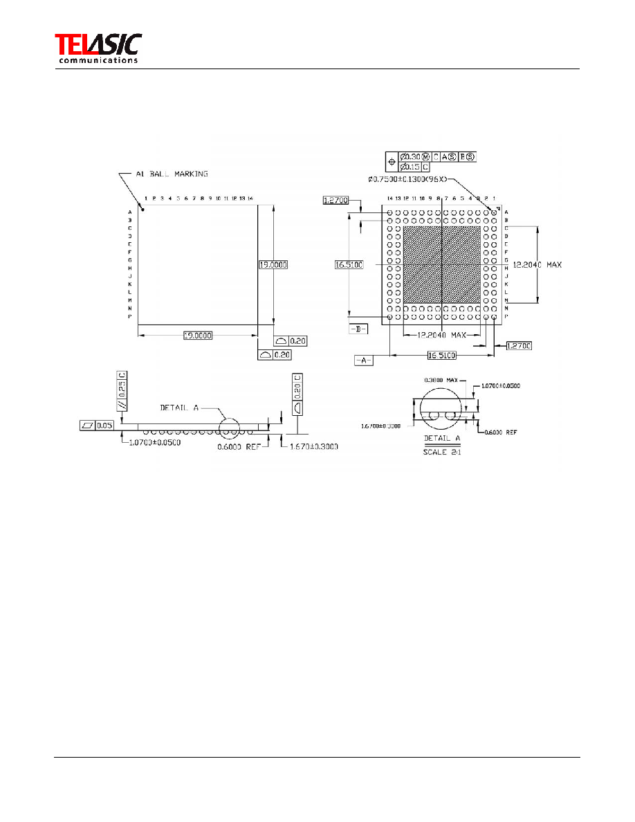
MKDSTC2411 Rev-
Figure 19: TC2411
96 Ball, Cavity-Down BGA Package Outline Dimensions (mm)
The information in this document is believed to be accurate in all respects at the time of publication but is subject to change without notice.
TelASIC assumes no responsibility for errors and omissions, and disclaims responsibility for any consequences resulting from the use of
information included herein. Additionally, TelASIC assumes no responsibility for the functioning of undescribed features or parameters. TelA-
SIC reserves the right to make changes without further notice. TelASIC makes no warranty, representation or guarantee out of the application
or use of any product or circuit, and specifically disclaims any and all liability, intended, or authorized for use in applications intended to sup-
port or sustain life, or for any other application in which the failure of the TelASIC product could create a situation where personal injury or
death may occur. Should Buyer purchase or use TelASIC products for any such unintended or unauthorized application, Buyer shall indem-
nify and hold TelASIC harmless against all claims and damages.