U4790B
TELEFUNKEN Semiconductors
Rev. A2, 03-Dec-97
1 (5)
Automotive Lamp-Outage Monitor, V
T
= 8 mV, V
Z(3,5)
= 22 V
Description
The bipolar IC U4790B is designed as a monitor for lamp
failure in automobiles. The comparator threshold is
matched to the PTC characteristic of incandescent lamps.
The threshold is tied to a typical value of V
4,6
= V
S
≠ V
T
where V
T
= 8 mV.
If the voltage drop across shunt resistor, R
sh
, exceeds
8 mV, the output is turned off, otherwise the output is
turned on. Without supply voltage or open input Pin 8, the
output is turned off. An unused comparator input must be
connected to Pin 7.
Features
D 10 kV≠ESD protection
D Two comparators with common reference
D Tight threshold tolerance
D Threshold matched to PTC characteristic
of incandescent lamps
D Temperature compensated
D NPN output
D Interference and damage≠protection
according to VDE 0839
D EMI protection
D Reversal polarity protection
D Load-dump protection
Ordering Information
Extended Type Number
Package
Remarks
U4790B
DIP8
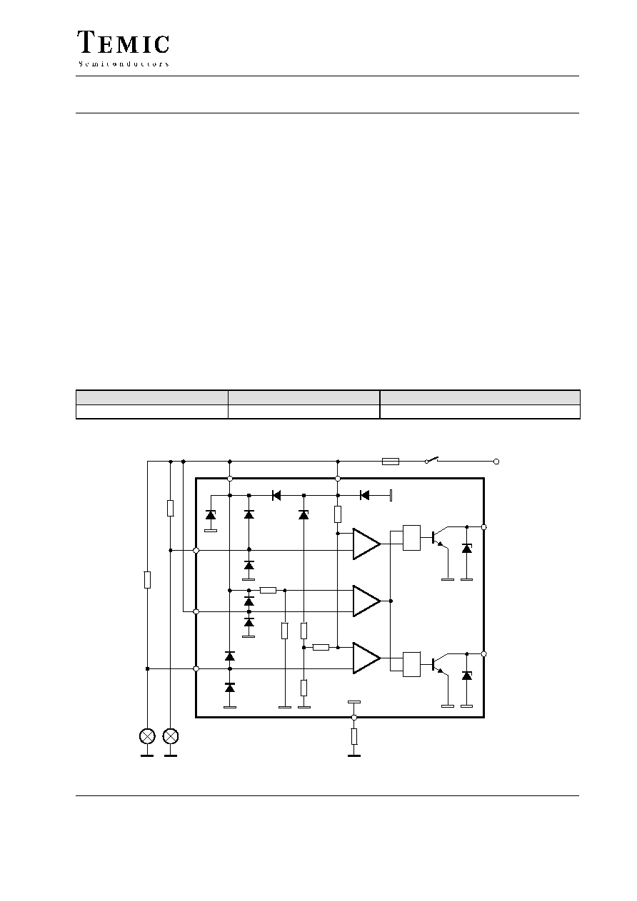
Block Diagram
≠
+
≠
+
≠
+
&
&
Z
2
2
7
4
8
6
5
3
1
R
1
150
W
V
S
V
Batt
R
sh
R
sh
Lamps
95 10606
0.6 V
S
OUT1
OUT2
Z
5
Z
3
Figure 1. Schematic and application circuit

U4790B
TELEFUNKEN Semiconductors
Rev. A2, 03-Dec-97
3 (5)
Electrical Characteristics
V
S
= 9 to 15 V, T
amb
= ≠40 to +95
∞
C, figure 1, unless otherwise specified
Parameters
Test Conditions / Pin
Symbol
Min
Typ
Max
Unit
Supply voltage
Pin 2,7
V
S
9
15
V
Internal Z diode Z
2
Pin 2
V
Z
20
V
Current consumption
V
S
= 12 V
Pin 1
measured at Pin 1 (GND)
I
1
4.5
6
mA
Output saturation voltage
V
S
= 9 V, I
3,5
= 10 mA
T
amb
= 25
∞
C
Pin 3,5
V
sat
0.5
V
Output Z diodes Z
3
, Z
5
Pin 3,5
V
Z
21
V
Control signal threshold
Reference point Pin 7 (V
7
)
I
3,5
= 3 mA
Pin 4,6
V
S
= 12 V
V
S
= 15 V
≠V
T
6.5
7.8
8
9.3
9.5
10.8
mV
Voltage drift
DV +
V
T(15V)
* V
T(12V)
15 V
* 12V
Pin 4,6
DV
0.45
mV/V
Threshold voltage
Switch identification Pin 8
V
8
0.6 V
S
V
Input currents
Pin 4,6
I
I
100
nA
Pin 8
5
mA
Delay time
Switch-on
Pin 3,5
High to low
t
d(on)
6
ms
Switch-off
Low to high
t
d(off)
30
ms
12.00
11.95
12
V
4,6
V
0
t
d(off)
t
d(on)
10
20
30
40
50
60
ms
0
t
95 10624
V
V
6
Figure 3.
U4790B
TELEFUNKEN Semiconductors
Rev. A2, 03-Dec-97
5 (5)
Ozone Depleting Substances Policy Statement
It is the policy of TEMIC TELEFUNKEN microelectronic GmbH to
1. Meet all present and future national and international statutory requirements.
2. Regularly and continuously improve the performance of our products, processes, distribution and operating systems
with respect to their impact on the health and safety of our employees and the public, as well as their impact on
the environment.
It is particular concern to control or eliminate releases of those substances into the atmosphere which are known as
ozone depleting substances ( ODSs ).
The Montreal Protocol ( 1987 ) and its London Amendments ( 1990 ) intend to severely restrict the use of ODSs and
forbid their use within the next ten years. Various national and international initiatives are pressing for an earlier ban
on these substances.
TEMIC TELEFUNKEN microelectronic GmbH semiconductor division has been able to use its policy of
continuous improvements to eliminate the use of ODSs listed in the following documents.
1. Annex A, B and list of transitional substances of the Montreal Protocol and the London Amendments respectively
2 . Class I and II ozone depleting substances in the Clean Air Act Amendments of 1990 by the Environmental
Protection Agency ( EPA ) in the USA
3. Council Decision 88/540/EEC and 91/690/EEC Annex A, B and C ( transitional substances ) respectively.
TEMIC can certify that our semiconductors are not manufactured with ozone depleting substances and do not contain
such substances.
We reserve the right to make changes to improve technical design and may do so without further notice.
Parameters can vary in different applications. All operating parameters must be validated for each customer
application by the customer. Should the buyer use TEMIC products for any unintended or unauthorized
application, the buyer shall indemnify TEMIC against all claims, costs, damages, and expenses, arising out of,
directly or indirectly, any claim of personal damage, injury or death associated with such unintended or
unauthorized use.
TEMIC TELEFUNKEN microelectronic GmbH, P.O.B. 3535, D-74025 Heilbronn, Germany
Telephone: 49 ( 0 ) 7131 67 2831, Fax number: 49 ( 0 ) 7131 67 2423

