Product Specification
July 24, 2002
Revision 0.52 Preview
U
LTRA
C
HIP
The Coolest LCD Driver. Ever!!
128COM x 240SEG Matrix LCD Controller-Driver
H
IGH
-V
OLTAGE
M
IXED
-S
IGNAL
IC

UC1608
128x240 Matrix LCD Controller-Drivers
(Revision 0.52 Preview)
1
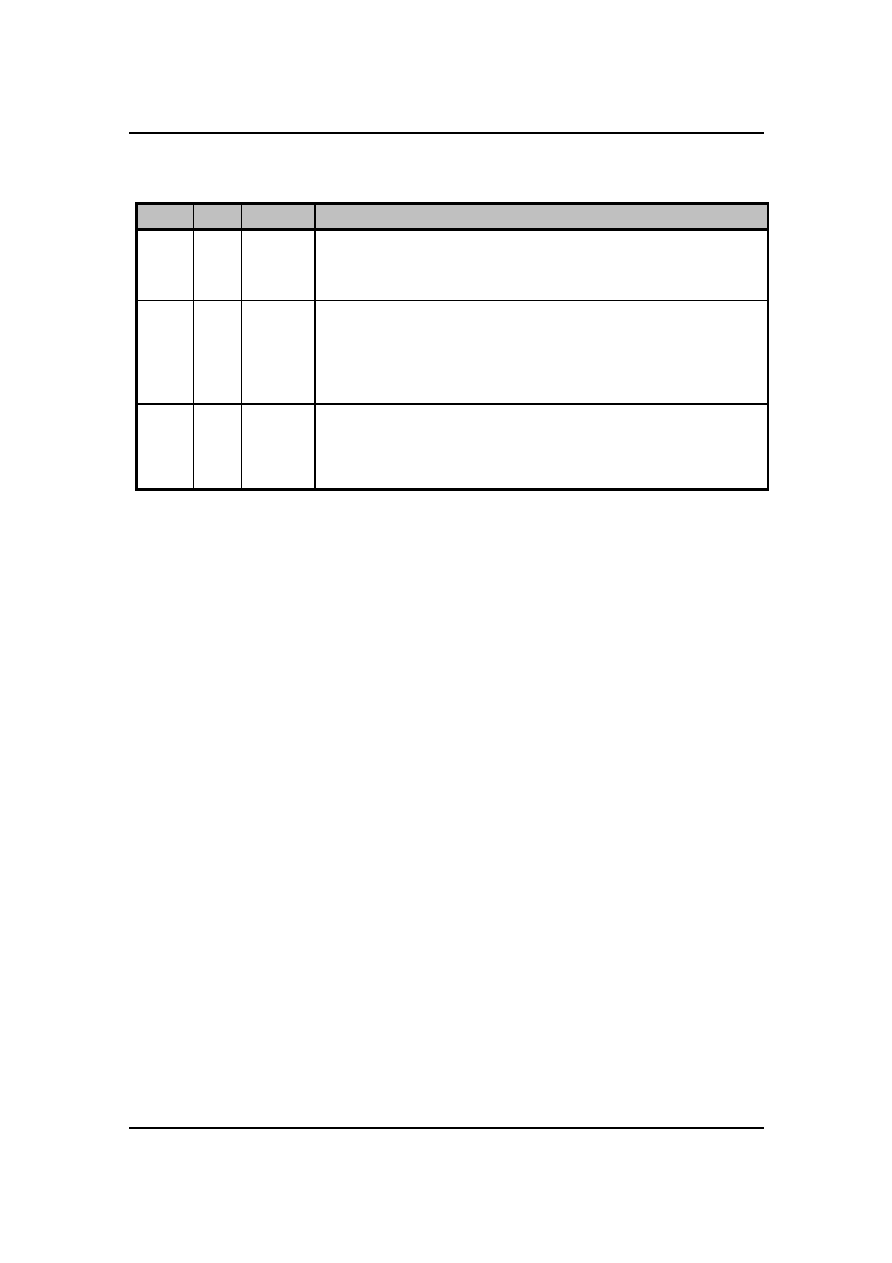
Table Of Revision History
Version
Contents
Date of revision
0.52
First release
July 24,2002

U
LTRA
C
HIP
High-Voltage Mixed-Signal IC
�1999-2002
2
Revision 0.52
Table of Content
Introduction ...........................................................................................................1
Ordering Information .............................................................................................2
Block Diagram.......................................................................................................3
Pin Description......................................................................................................4
Control Registers ..................................................................................................7
Command Summary .............................................................................................9
Command description .........................................................................................10
LCD Voltage Setting ...........................................................................................15
V
LCD
Quick Reference .........................................................................................16
LCD Display Controls..........................................................................................17
Host Interface .....................................................................................................19
Display Data RAM...............................................................................................20
Reset & Power Management ..............................................................................23
Absolute Maximum Ratings ................................................................................27
Specifications......................................................................................................28
AC Characteristics ..............................................................................................29
Physical Dimensions...........................................................................................32
Pad Coordinates .................................................................................................33

UC1608
128x240 Matrix LCD Controller-Drivers
(Revision 0.52 Preview)
1
UC1608
Single-Chip, Ultra-Low Power
128COM x 240SEG Matrix
Passive LCD Controller-Driver
I
NTRODUCTION
UC1608 is an advanced high-voltage mixed-
signal CMOS IC, especially designed for the
display needs of ultra-low power hand-held
devices.
This chip employs UltraChip's unique DCC
(Direct Capacitor Coupling) driver architecture to
achieve near crosstalk free images.
In addition to low power COM and SEG drivers,
UC1608 contains all necessary circuits for high-V
LCD power supply, bias voltage generation,
timing generation and graphics data memory.
Advanced circuit design techniques are
employed to minimize external component counts
and reduce connector size while achieving
extremely low power consumption.
M
AIN
A
PPLICATIONS
�
Cellular Phones, Smart Phones, PDA and
other battery operated palm top devices
and/or portable Instruments
F
EATURE
H
IGHLIGHTS
�
Single chip controller-driver supports 128
COM x 240 SEG LCD, with vertical scroll.
�
Support industry standard 8080 or 6800 bus
protocol in either 8-bit or 4-bit parallel
interface.
�
Support two multiplexing rates (128, 96).
�
Self-configuring 8x charge pump with on-
chip pumping capacitor requires only 5
external capacitors to operate.
�
Flexible data addressing/mapping schemes
to support wide ranges of software models
and LCD layout placements.
�
Software programmable 4 temperature
compensation coefficients.
�
On-chip bypass capacitor for V
LCD
makes
V
LCD
bypass capacitor optional for small
LCD panels.
�
On-chip Power-ON Reset and Software
RESET commands, make RST pin optional.
�
V
DD
(digital) range: 2.4V ~ 3.3V
V
DD
(analog) range: 2.4V ~ 3.3V
LCD V
OP
range:
6.5V ~ 15V
�
Available in gold bump dies
Bump pitch: 50uM min.
Bump gap: 18uM min.

U
LTRA
C
HIP
High-Voltage Mixed-Signal IC
�1999-2002
2
Revision 0.52
O
RDERING
I
NFORMATION
Product ID
Description
UC1608xGAC
Gold bumped die.
UC1608xFAC COF
packaging.
General Notes
A
PPLICATION
I
NFORMATION
For improved readability, the specification contains many application data points. When application information is given, it
is advisory and does not form part of the specification for the device.
B
ARE
D
IE
D
ISCLAIMER
All die are tested and are guaranteed to comply with all data sheet limits up to the point of wafer sawing for a period of
ninety (90) days from the date of UltraChip's delivery. There is no post waffle saw/pack testing performed on individual die.
Although the latest modern processes are utilized for wafer sawing and die pick-&-place into waffle pack carriers,
UltraChip has no control of third party procedures in the handling, packing or assembly of the die. Accordingly, it is the
responsibility of the customer to test and quality their application in which the die is to be used. UltraChip assumes no
liability for device functionality or performance of the die or systems after handling, packing or assembly of the die.
L
IFE
S
UPPORT
A
PPLICATIONS
These devices are not designed for use in life support appliances, or systems where malfunction of these products can
reasonably be expected to result in personal injuries. Customer using or selling these products for use in such
applications do so at their own risk.

UC1608
128x240 Matrix LCD Controller-Drivers
(Revision 0.52 Preview)
3
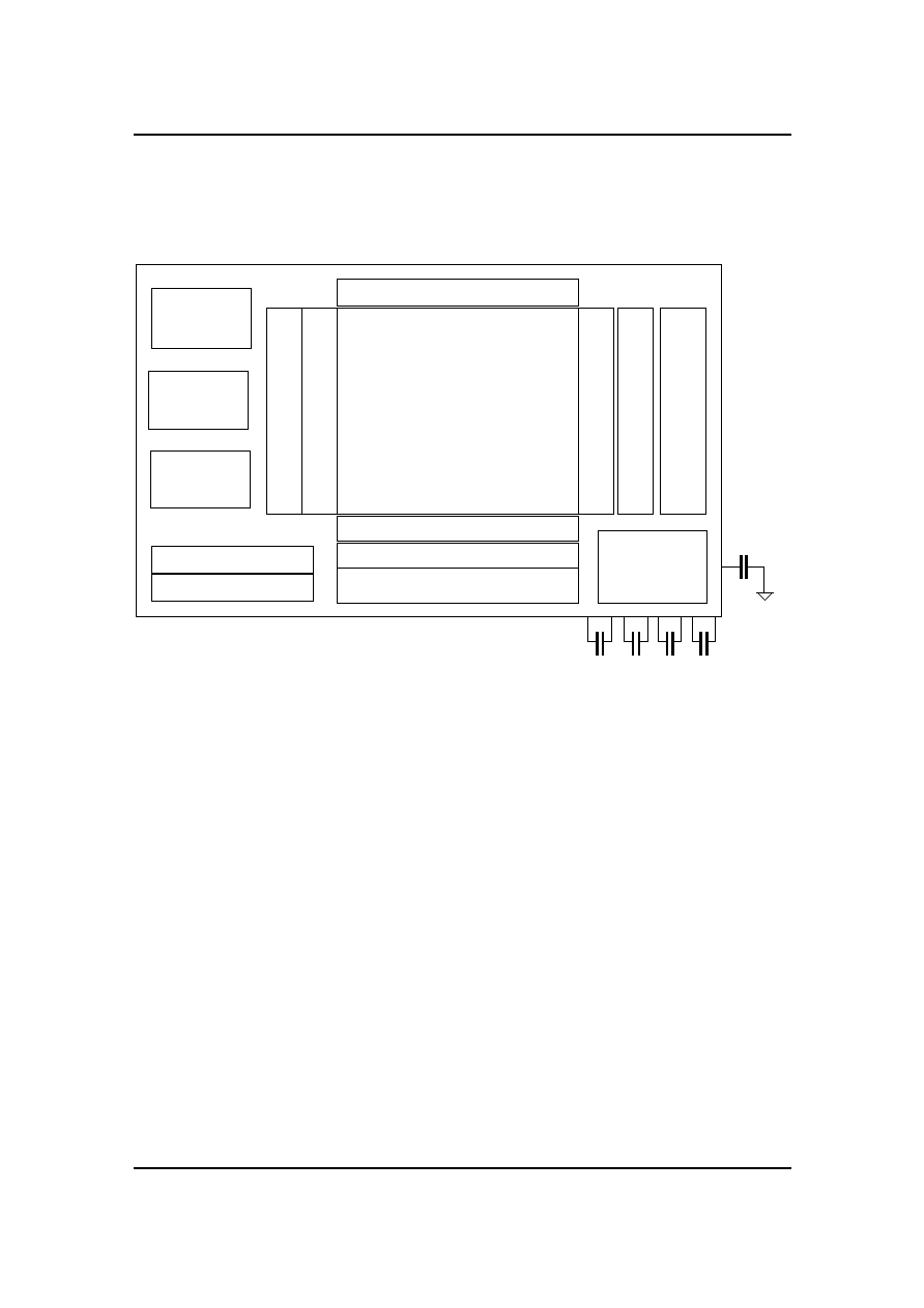
B
LOCK
D
IAGRAM
CO
M DRI
V
E
R
S
SEG DRIVERS
POWER-ON
& RESET
CONTROL
R
O
W
AD
DR
ESS G
E
NER
A
TO
R
CLOCK &
TIMING
GEN.
HOST INTERFACE
CONTROL &
STATUS
REGISTER
COMMAND
COLUMN ADDRESS GENERATOR
DISPLAY DATA RAM
DISPLAY DATA LATCHES
LEVEL SHIFTERS
LE
VEL SH
IFTER
V
LCD
& BIAS
GENERATOR
PAG
E ADD
R
ESS GEN
E
R
A
TO
R
D
A
TA RA
M I
/
O
BUF
F
ER
C
B0
C
LCD
C
B1
C
B2
C
B3

U
LTRA
C
HIP
High-Voltage Mixed-Signal IC
�1999-2002
4
Revision 0.52
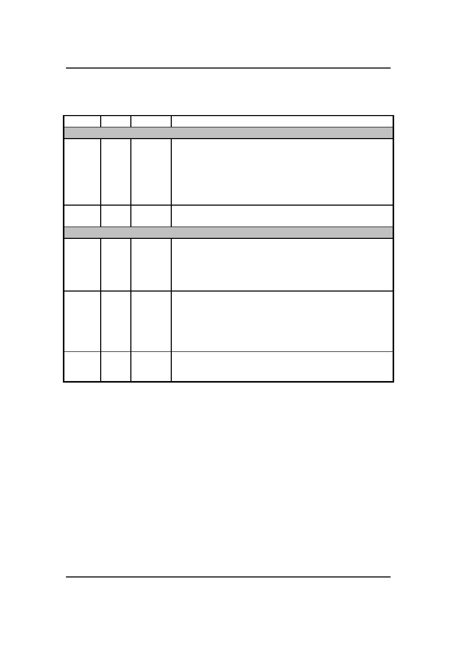
P
IN
D
ESCRIPTION
Name Type Pins
Description
M
AIN
P
OWER
S
UPPLY
V
DD
V
DD2
V
DD3
PWR
V
DD2
/V
DD3
is the analog V
DD
and it should be connected to the same
power source. V
DD
is the digital V
DD
and is connected to a voltage
source that is the same, or lower than V
DD2
/V
DD3
.
V
DD
supplies for digital logic and display data RAM.
V
DD2
supplies for V
LCD
and V
BIAS
generator, V
DD3
supplies for other
analog circuits.
Minimize the trace resistance for V
DD
and V
DD2
.
V
SS
V
SS2
GND
Ground.
Connect
V
SS
and V
SS2
to the shared GND pin.
Minimize the trace resistance for V
SS
and V
SS2
.
LCD P
OWER
S
UPPLY
V
B3+
V
B3�
V
B2+
V
B2�
V
B1+
V
B1�
V
B0+
V
B0�
PWR
LCD Bias Voltages. These are the voltage source to provide SEG
driving currents. These voltages are generated internally. Connect
capacitors of C
BX
value between V
BX+
and V
BX�
.
The resistance of these four traces directly affects the SEG driving
strength of the resulting LCD module. Minimize the trace resistance is
critical in achieving high quality image.
S
B3+
S
B3�
S
B2+
S
B2�
S
B1+
S
B1�
S
B0+
S
B0�
I
The sensor pins for C
BX
capacitors. Please connect these sensor pins
as closely to proper C
BX
pads as possible. These signals can tolerate
input resistance of up to 2K Ohm, so, narrow COF traces can be used.
However, the noise on these pins affects the accuracy of SEG driving
voltage level. To minimize noise caused by V
BX
-C
BX
charging current,
the trace resistance shared between V
BX+/-
and S
BX+/-
should be
minimized.
V
LCD-IN
V
LCD-OUT
PWR
Main LCD Power Supply. Connect these pins together.
A by-pass capacitor C
L
is optional. When C
L
is used, connect C
L
between V
LCD
and V
SS
, and keep the trace resistance under 300 Ohm.
N
OTE
�
Recommended capacitor values:
C
B
: ~100x LCD load capacitance or 1.5uF (2V), whichever is higher.
C
L
: 10nF ~ 50nF (16V) is appropriate for most applications.

UC1608
128x240 Matrix LCD Controller-Drivers
(Revision 0.52 Preview)
5
Name Type Pins
Description
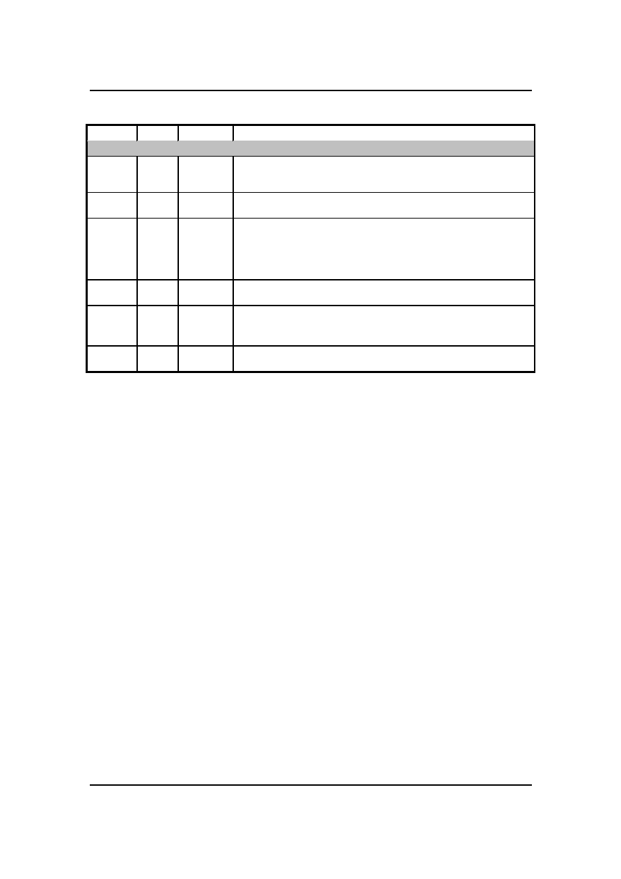
H
OST
I
NTERFACE
BM[1:0] I
Parallel/Serial.
4-bit bus modes: "LL": 8080
"LH": 6800
8-bit bus modes: "HL": 8080
"HH": 6800
CS I
Chip Select. The chip is selected when CS="H". When the chip is not
selected, D[7:0] will be high impedance.
RST I
When RST="L", all control registers are re-initialized by their default
states. Since UC1608 has built-in Power-ON-Reset and Software Reset
command, RST pin is not required for proper chip operation.
When RST pin is used, insert a 5~10K Ohm resistor to improve noise
filtering. When RST is not used, connect the pin to V
DD
.
CD I
Select Command or Display Data for read/write operation.
"L": Command
"H": Display data
WR0
WR1
I
WR[1:0] controls the read/write operation of the host interface.
In parallel mode, WR[1:0] meaning depends on whether the interface is
in the 6800 mode or the 8080 mode.
D0~D7 I/O
Bi-directional bus for both serial and parallel host interfaces.
In 4-bit bus mode, connect unused pins to V
DD
or V
SS
.

U
LTRA
C
HIP
High-Voltage Mixed-Signal IC
�1999-2002
6
Revision 0.52
Name Type Pins
Description
LCD D
RIVER
O
UTPUT
SEG1 ~
SEG240
HV
SEG (column) driver outputs. Support up to 240 columns.
Leave unused drivers open-circuit.
COM1 ~
COM128
HV
COM (row) driver outputs. Support up to 128 rows. When Mux Rate is
not 128, please use only COM1~COM(x), x=128, or 96, and leave COM
(x+1) ~ COM128 open-circuit.
M
ISC
. P
INS
TST4
I
Test control. Connect to V
SS
.
TST[3:1]
I/O
Test I/O pins. Leave these pins open circuit during normal use.
TP[3:1]
I
Test control. Leave these pins open circuit during normal use.

UC1608
128x240 Matrix LCD Controller-Drivers
(Revision 0.52 Preview)
7
C
ONTROL
R
EGISTERS
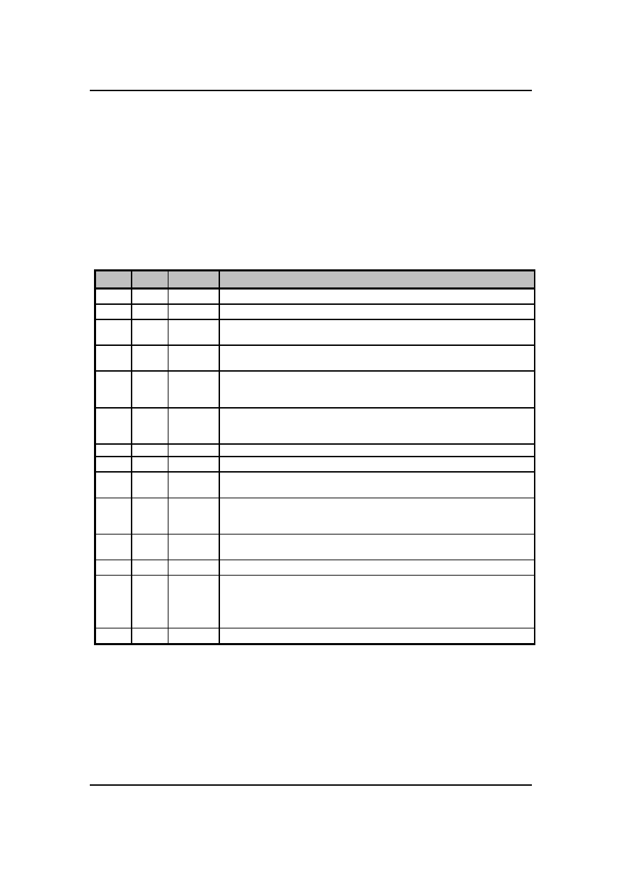
UC1608 contains registers which control the chip operation. These registers can be modified by commands.
The following table is a summary of the control registers, their meaning and their default value. The
commands supported by UC1608 are described in the next two sections, first a summary table, followed by
a detailed description.
Name: The Symbolic reference of the register byte.
Note that, some symbol names refer to collection of bits (flags) within one register byte.
Default: Numbers shown in Bold fonts are values after Power-Up-Reset and System-Reset..
Name
Bits
Default
Description
SL
6
0H
Start Line. Mapping from COM1 to Display Data RAM.
CR
8
0H
Return Column Address. Useful for cursor implementation.
CA 8 0H
Display Data RAM Column Address
(Used in Host to Display Data RAM access)
PA 4 0H
Display Data RAM Page Address
(Used in Host to Display Data RAM access)
BR
2
2H
Bias Ratio. The ratio between V
LCD
and V
BIAS
.
00b= 10.7
01b= 11.3
10b=12.0
11b=
12.7
TC 2 0H
Temperature Compensation (per
o
C).
00b: 0.0%
01b: -0.05%
10b: -0.1%
11b: -0.2%
GN
2
3H
Gain, coarse setting of V
BIAS
and V
LCD
PM
6
0H
Electronic Potentiometer to fine tune V
BIAS
and V
LCD
MR 1 1H
Multiplexing Rate: Number of pixel rows:
0b: 96
1b: 128
OM 2
� Operating Modes (Read Only)
10b: Sleep
11b: Normal
01b: (Not used)
00b: Reset
BZ 1
� Busy with internal processes (reset, changing mode, etc.)
OK for Display RAM read/write access.
RS
1
�
Reset in progress, Host Interface not ready
PC
3
7H
Power Control and panel loading.
PC[0]: 0b: LCD: <20nF
1b: LCD: >20nF
PC[2:1]: 00b: External V
LCD
11b: Internal V
LCD
01b and 10b are reserved, for UltraChip only. Please do not use.
APC0
8
2CH
Advanced Product Configuration. For UltraChip only. Please do not use.

U
LTRA
C
HIP
High-Voltage Mixed-Signal IC
�1999-2002
8
Revision 0.52
Name
Bits
Default
Description
DC 3 00H
Display
Control:
DC[0]: PXV: Pixels Inverse (Default OFF)
DC[1]: APO: All Pixels ON (Default OFF)
DC[2]: Display ON/OFF (Default OFF).
AC
4
0H
Address Control:
AC[0]: WA: Automatic column/page Wrap Around (Default 0:OFF)
AC[1]: Reserved (always set to 0)
AC[2]: PID: PA (page address) auto increment direction (0: +1 1: -1)
AC[3]: CUM: Cursor update mode, (Default 0:OFF)
when CUM=1, CA increment on write only, wrap around suspended
LC 4
00H
LCD Mapping Control:
LC[0]: MSF: MSB First mapping Option
LC[1]: Reserved (always set to 0)
LC[2]: MX, Mirror X (Column sequence inversion)
LC[3]: MY, Mirror Y (Row sequence inversion)

UC1608
128x240 Matrix LCD Controller-Drivers
(Revision 0.52 Preview)
9
C
OMMAND
S
UMMARY
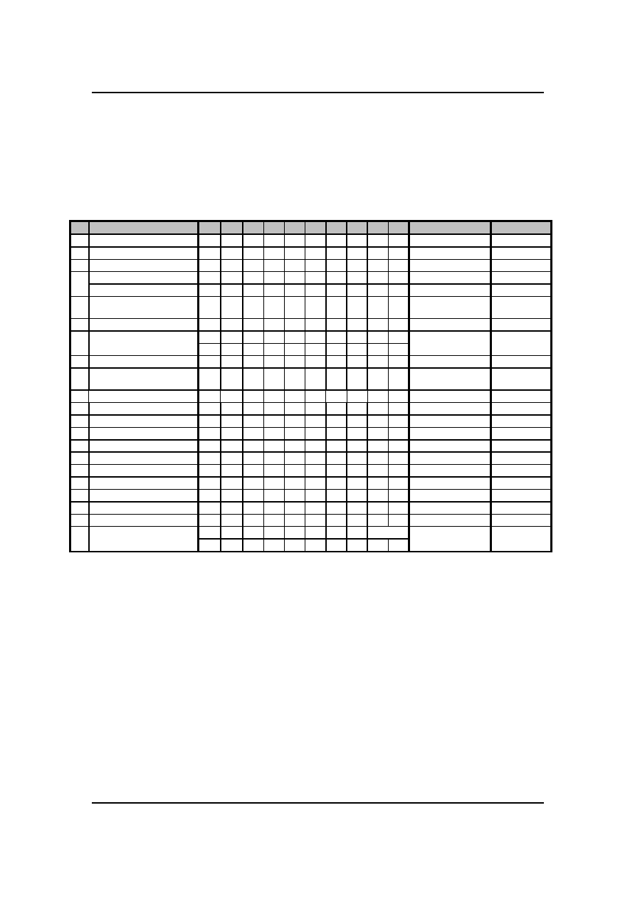
The following is a list of host commands supported by UC1608
C/D: 0: Control,
1: Data
W/R: 0: Write Cycle,
1: Read Cycle
# Useful Data bits
� Don't Care
Command
C/D W/R D7 D6 D5 D4 D3 D2 D1 D0
Action
Default value
1 Write Data Byte
1
0
#
#
#
#
#
#
#
#
Write 1 byte
N/A
2
Read
Data
Byte
1 1 # # # # # # # #
Read
1
byte
N/A
3 Get
Status
0 1 BZ MX DE RS WA
GN1 GN0
1
Get Status
N/A
Set Column Address LSB
0
0
0
0
0
0
#
#
#
#
Set CA[3:0]
0
4
Set Column Address MSB
0
0
0
0
0
1
#
#
#
#
Set CA[7:4]
0
5
Set Mux Rate and
temperature compensation.
0 0 0 0 1 0 0 # # # Set
{MR,
TC[1:0]}
MR: 1
TC: 0
6
Set
Power
Control
0 0 0 0 1 0 1 # # #
Set
PC[2:0]
111b
0 0 0 0 1 1 0 0 0 R
7
Set Adv. Product Config.
(double byte command)
0 0 # # # # # # # #
For UltraChip only.
Do not use.
N/A
8 Set Start Line
0
0
0
1
#
#
#
#
#
#
Set SL[5:0]
0
9
Set Gain and Potentiometer
(double-byte command)
0
0
0
0
1
#
0
#
0
#
0
#
0
#
0
#
0
#
1
#
Set {GN[1:0],
PM[5:0]}
GN=3
PM=0
10 Set RAM Address Control
0
0
1
0
0
0
1
#
#
#
Set AC[2:0]
000b
11
Set
All-Pixel-ON
0 0 1 0 1 0 0 1 0 #
Set
DC[1]
0=disable
12
Set
Inverse
Display
0 0 1 0 1 0 0 1 1 #
Set
DC[0]
0=disable
13
Set
Display
Enable
0 0 1 0 1 0 1 1 1 #
Set
DC[2]
0=disable
14
Set
Page
Address
0 0 1 0 1 1 # # # #
Set
PA[3:0]
0
15 Set LCD Mapping Control
0
0
1
1
0
0
#
#
#
#
Set LC[3:0]
0
16
System
Reset
0 0 1 1 1 0 0 0 1 0 System
Reset
N/A
17
NOP
0 0 1 1 1 0 0 0 1 1 No
operation
N/A
18 Set LCD Bias Ratio
0
0
1
1
1
0
1
0
#
#
Set BR[1:0]
10b=12
19
Reset
Cursor
Mode
0 0 1 1 1 0 1 1 1 0 AC[3]=0,
CA=CR
N/A
20
Set
Cursor
Mode
0 0 1 1 1 0 1 1 1 1 AC[3]=1,
CR=CA
N/A
0 0 1 1 1 0 0 1 TT
21
Set Test Control
(double byte command)
0 0 # # # # # # # #
For UltraChip only.
Do not use.
N/A
* Other than commands listed above, all other bit patterns may result in undefined behavior.

U
LTRA
C
HIP
High-Voltage Mixed-Signal IC
�1999-2002
10
Revision 0.52
C
OMMAND DESCRIPTION
(1) Write data to display memory
Action
C/D W/R D7 D6 D5 D4 D3 D2 D1 D0
Write data
1
0
8bits data write to SRAM
(2) Read data to display memory
Action
C/D W/R D7 D6 D5 D4 D3 D2 D1 D0
Read data
1
1
8bits data from SRAM
Write/Read Data Byte ( command 1,2 ) operations access display buffer RAM based on Page Address (PA)
register and Column Address (CA) register. To minimize bus interface cycles, PA and CA will be
incremented automatically depending on the setting of Access Control (AC) registers. PA and CA can also
be programmed directly by issuing Set Page Address and Set Column Address commands.
If Wrap-Around (WA) is OFF (AC[0] = 0), CA will stop increasing after reaching the end of page (MC), and
system programmers need to set the values of PA and CA explicitly. If WA is ON (AC[0]=1), when CA
reaches end of page, CA will be reset to 0 and PA will be increased or decrease by 1, depending on the
setting of Page Increment Direction (PID, AC[2]). When PA reaches the boundary of RAM (i.e. PA = 0 or 15),
PA will be wrapped around to the other end of RAM and continue.
(3) Get Status
Action
C/D W/R D7 D6 D5 D4 D3 D2 D1 D0
Get Status
0
1
BZ MX DE RS WA GN1 GN0 1
Status flag definitions:
BZ: Busy with internal process. When BZ=1 host interface can access if RS=0.
MX: Status of register LC[1], mirror X.
DE: Display enable flag. DE=1 when display enabled
RS: Reset in progress. If RS=1.host interface will be inaccessible.
WA: status of register AC[0] .automatic column/page wrap around.
GN0,1:GN[1:0] .register Gain
(4) Set Column Address
Action
C/D W/R D7 D6 D5 D4 D3 D2 D1 D0
Set Column Address LSB CA[3:0]
0
0
0 0 0 0
CA3 CA2 CA1 CA0
Set Column Address MSB CA[7:4]
0
0
0 0 0 1
CA7 CA6 CA5 CA4
Set the SRAM column address before Write/Read memory from host interface.
CA possible value=0-239

UC1608
128x240 Matrix LCD Controller-Drivers
(Revision 0.52 Preview)
11
(5) Set Multiplex Rate and Temperature Compensation
Action
C/D W/R D7 D6 D5 D4 D3 D2 D1 D0
Set Multiplex Rate MR
Set Temperature Compensation TC[1:0]
0 0 0 0 1 0 0 MR
TC1
TC0
Set the multiplex ratio (number of rows) and temperature compensation.
MUX ratio definition:
0b=96
1b=128
Temperature compensation curve definition:
00b= -0.00%/C 01b= -0.05%/C 10b= -0.10%/C 11b= -0.20%/C
(6) Set Power Control
Action
C/D W/R D7 D6 D5 D4 D3 D2 D1 D0
Set Panel Loading PC[2:0]
0
0
0 0 1 0 1
PC2 PC1 PC0
Set PC[0] according to the capacitance loading of LCD panel.
0b: <=20nF
1b: >20nF
Set PC[2:1] to program to use internal charge pump of external VLCD source:
00b=External VLCD
11b=Internal VLCD
(7) Set Advance Product Configuration
Action
C/D W/R D7 D6 D5 D4 D3 D2 D1 D0
0 0 0 0 1 1 0 0 0 R
Set APC
(Double byte command)
0
0
APC register parameter
For UltraChip only. Please Do NOT use.
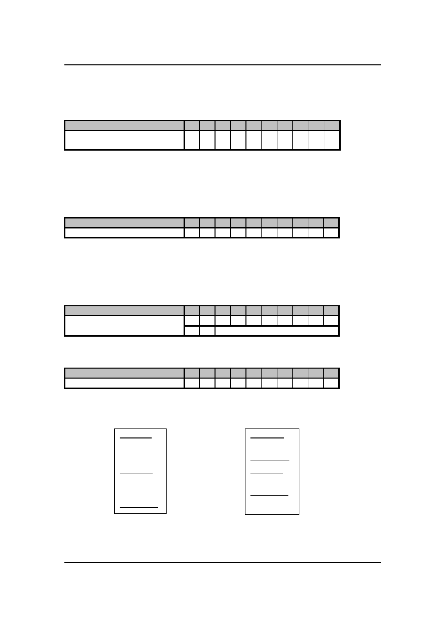
(8) Set Start Line
Action
C/D W/R D7 D6 D5 D4 D3 D2 D1 D0
Set Start Line SL[5:0]
0
0
0 1
SL5 SL4 SL3 SL2 SL1 SL0
Set the start line number
Start line setting will scroll the displayed image up by SL rows. The valid value is between 0 (no
scrolling) and 63. One example of the visual effect on LCD is illustrated in the figure below.
0 0
N N
SL=0
SL=N
Image row 0
..........
Image row N
..........
Image row 127
Image row N
..........
Image row 127
Image row 0
.........
image row N-1

U
LTRA
C
HIP
High-Voltage Mixed-Signal IC
�1999-2002
12
Revision 0.52
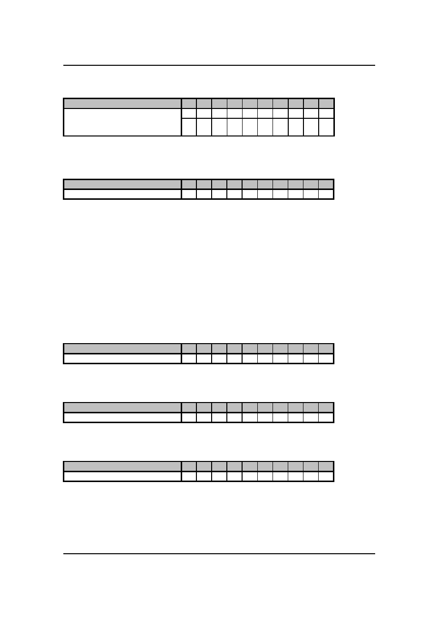
(9) Set Gain and Potentiometer
Action
C/D W/R D7 D6 D5 D4 D3 D2 D1 D0
0 0 1 0 0 0 0 0 0 1
Set Gain and Potentiometer
GN [1:0] PM [5:0]
(Double byte command)
0
0 GN1 GN0 PM5 PM4 PM3 PM2 PM1 PM0
Program Gain (GN[1:0]) and Potentiometer (PM[5:0]). See section LCD V
OLTAGE
S
ETTING
for more detail.
Effective range of GN = 0 ~ 3
PM value = 0 ~ 63
(10) Set RAM Address Control
Action
C/D W/R D7 D6 D5 D4 D3 D2 D1 D0
Set AC [2:0]
0
0
1 0 0 0 1
AC2 AC1 AC0
Program registers AC[2:0] for RAM address control.
AC[0] - WA, Automatic column/page wrap around.
0: CA or PA (depends on AC[1]= 0 or 1) will stop incrementing after reaching boundary
1: CA or PA (depends on AC[1]= 0 or 1) will restart, and PA or CA will increment by one step.
AC[1] � Auto-Increment order
0 : column (CA) increment (+1) first until CA reach CA boundary, then PA will increment by (+/-1).
1 : page (PA) increment (+/-1) first until PA reach PA boundary, then CA will increment by (+1) .
AC[2] � PID, page address (PA) auto increment direction ( 0/1 = +/- 1 )
When WA=1, controls whether page address will be adjusted by +1 or -1, when CA reached CA
boundary. No effect when WA=0.
CA boundary is 240 and PA boundary is 15 when PID=0, PA boundary is 0 when PID=1.
(11) Set All Pixel ON
Action
C/D W/R D7 D6 D5 D4 D3 D2 D1 D0
Set All Pixel On DC [1]
0
0
1 0 1 0 0 1 0
DC1
Set DC[1] to force all SEG drivers to output ON signals. This function has no effect on the existing data
stored in display RAM.
(12) Set Inverse Display
Action
C/D W/R D7 D6 D5 D4 D3 D2 D1 D0
Set Inverse Display DC [0]
0
0
1 0 1 0 0 1 1
DC0
Set DC[0] to force all SEG drivers to output the inverse of the data stored in display memory. This function
has no effect on the existing data stored in display RAM.
(13) Set Display Enable
Action
C/D W/R D7 D6 D5 D4 D3 D2 D1 D0
Set Display Enable DC[2]
0
0
1 0 1 0 1 1 1
DC2
This command is for programming registers DC[2].
When DC[2] is set to 0, the IC will put itself into Sleep mode. All drivers, voltage generation circuit and timing
circuit will be halted to conserve power. When DC[2] is set to 1, UC1608 will first exit from Sleep mode,
restore the power and then turn on COM drivers and SEG drivers. There is no other explicit user action or
timing sequence required to enter or exit the Sleep mode.

UC1608
128x240 Matrix LCD Controller-Drivers
(Revision 0.52 Preview)
13
(14) Set Page Address
Action
C/D W/R D7 D6 D5 D4 D3 D2 D1 D0
Set Page Address LSB PA [3:0]
0
0
1 0 1 1
PA3 PA2 PA1 PA0
Set the SRAM page address before write/read memory from host interface.
Effective range of value = 0 ~ 15
(15) Set LCD Mapping Control
Action
C/D W/R D7 D6 D5 D4 D3 D2 D1
D0
Set LCD Mapping Control LC[3:0]
0
0
1 1 0 0 MY MX - MSF
Set LC[3:0] for COM (row) mirror (MY), SEG (column) mirror (MX) and MSB first or LSB first options (MSF).
MY is implemented by reversing the mapping order between RAM and COM (row) electrodes. The data
stored in RAM is not affected by MY command. MY will have immediate effect on the display image.
MX is implemented by selecting the CA or 239-CA as write/read (from host interface) display RAM
column address so this function will only take effect after rewriting the RAM data
MSF is implemented by MSB-LSB swapping. When MSB first (LC[0] ) bit is set, data D[7:0] will be re-
aligned as D[0:7] then be stored to RAM.
(16) System Reset
Action
C/D W/R D7 D6 D5 D4 D3 D2 D1 D0
System Reset
0
0
1 1 1 0 0 0 1 0
This command will activate the system reset. The system will take about 5ms to reset
(17) NOP
Action
C/D W/R D7 D6 D5 D4 D3 D2 D1 D0
No operation
0
0
1 1 1 0 0 0 1 1
This command is used for "no operation".
(18) Set LCD Bias Ratio
Action
C/D W/R D7 D6 D5 D4 D3 D2 D1 D0
Set Bias Ratio BR [1:0]
0
0
1 1 1 0 1 0
BR1 BR0
Bias ratio definition:
00b= 10.7
01b=11.3
10b=12.0
11b=12.7
(19) Reset Cursor Mode
Action
C/D W/R D7 D6 D5 D4 D3 D2 D1 D0
Return to Cursor. AC[3]=0, CA=CR
0
0
1 1 1 0 1 1 1 0
This command is used to reset cursor update mode function. See description below.

U
LTRA
C
HIP
High-Voltage Mixed-Signal IC
�1999-2002
14
Revision 0.52
(20) Set Cursor Mode
Action
C/D W/R D7 D6 D5 D4 D3 D2 D1 D0
Set AC[3]=1 CR=CA
0
0
1 1 1 0 1 1 1 1
Set Cursor Mode command is used to turn on cursor update mode function. AC[3] will be set to 1, register
CR will be set to the value of register CA
When AC[3]=1, column address (CA) will only increment with write RAM operation but not on read RAM
operation. The address CA wraps around will also be suspended no matter what WA setting is. The
purpose of this combination of features is to support "Read-Modify-Write" for cursor implementation.
Reset Cursor Mode command will clear cursor update mode flag (AC[3]=0), CA will be restored to previous
CA value which is stored in CR, and CA, PA increment will return to its normal condition.
(21) Set Test Control
Action
C/D W/R D7 D6 D5 D4 D3 D2 D1 D0
0 0 1 1 1 0 0 1 TT
Set TT
(Double byte command)
0 0
Testing
parameter
This command is used for UltraChip production testing. For UltraChip Only. Please do not use.

UC1608
128x240 Matrix LCD Controller-Drivers
(Revision 0.52 Preview)
15
LCD V
OLTAGE
S
ETTING
M
ULTIPLEX
R
ATES
Multiplex Rates (MR) is software programmable.
Two MR is supported: 96, 128.
B
IAS
R
ATIO
S
ELECTION
Bias Ratio (BR) is defined as the ratio between
V
LCD
and V
BIAS
, i.e.
BR = V
LCD
/V
BIAS
,
where V
BIAS
= V
B1+
� V
B1�
= V
B0+
� V
B0�
.
The theoretical optimum Bias Ratio can be
estimated by
1
+
Mux
. In some applications, BR
is set to be 10~15% lower than the optimum value
calculated above in order to lower V
LCD
by 5~6%.
Such setting generally will not cause visible change
in image quality.
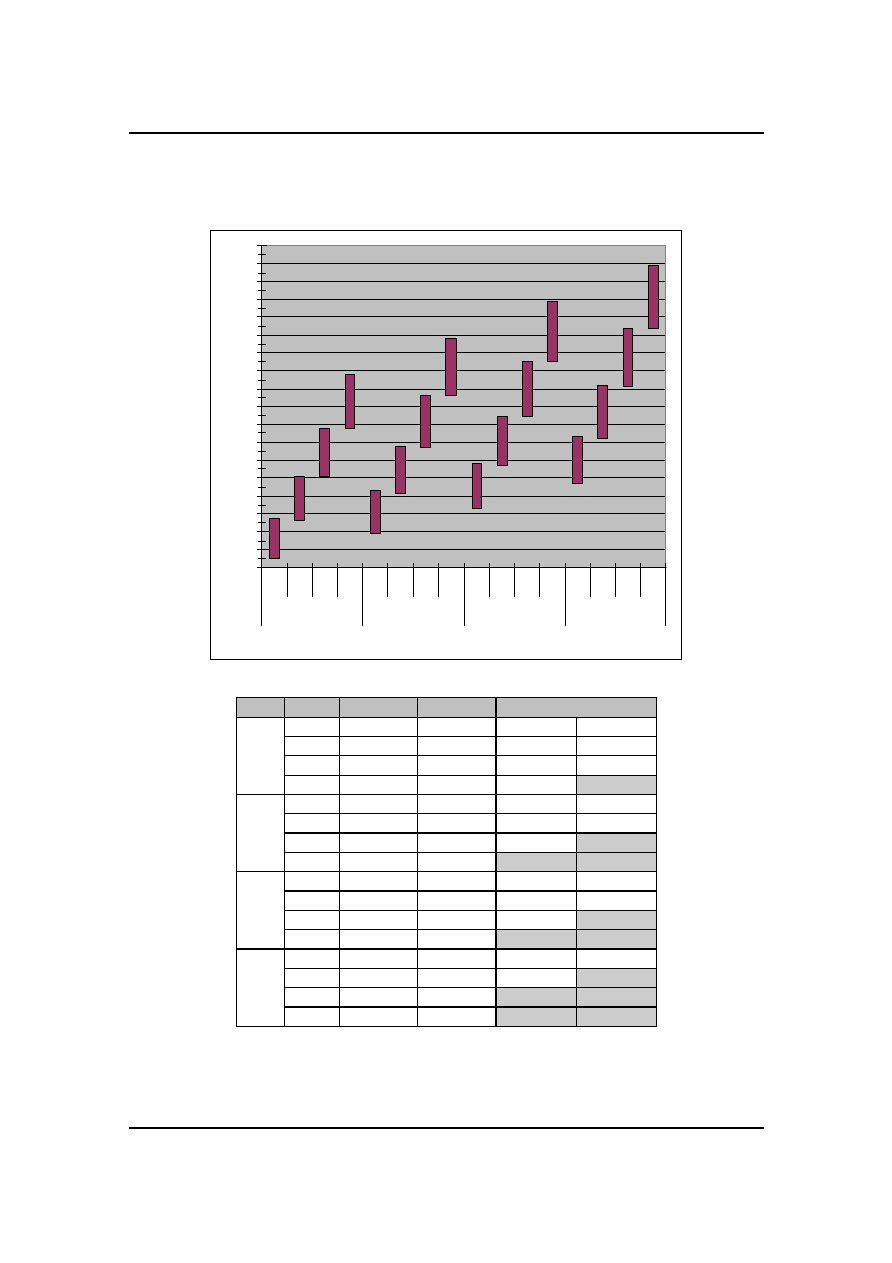
UC1608 supports four BR as listed below. BR can
be selected by software program.
BR
0
1
2
3
Bias Ratio 10.7 11.3
12
12.7
Table 2: Bias Ratios
T
EMPERATURE
C
OMPENSATION
Four (4) different temperature compensation
coefficients can be selected via software. The four
coefficients are given below:
TC
0
1
2
3
% per
o
C
0.0 �0.05 �0.10 �0.20
Table 4: Temperature Compensation
V
LCD
G
ENERATION
V
LCD
may be supplied either by internal charge
pump or by external power supply. The source of
V
LCD
is controlled by PC[2:1]. For good product
performance it is recommended to keep V
LCD
under
13V at room temperature.
When V
LCD
is generated internally, the voltage level
of V
LCD
is determined by four control registers: BR
(Bias Ratio), GN (Gain), PM (Potentiometer), and
TC (Temperature Compensation), with the
following relationship:
%)
)
25
(
1
(
)
(
0
T
PM
V
LCD
C
T
PM
C
C
V
�
-
+
�
�
+
=
where
C
V0
and C
PM
are two constants, whose value
depends on the BR-GN register setting. The
values are provided in the table on the next
page,
PM is the numerical value of PM register,
T is the ambient temperature in
O
C, and
C
T
is the temperature compensation coefficient
as selected by TC register.
L
OAD
D
RIVING
S
TRENGTH
The power supply circuit of UC1608 is designed to
handle LCD panels with load capacitance up to
~20nF when V
DD2
= 2.5V. For larger LCD panels
use higher V
DD
and COF packaging.

U
LTRA
C
HIP
High-Voltage Mixed-Signal IC
�1999-2002
16
Revision 0.52
V
LCD
Q
UICK
R
EFERENCE
11.00
11.50
12.00
12.50
13.00
13.50
14.00
14.50
15.00
15.50
16.00
16.50
17.00
17.50
18.00
18.50
19.00
19.50
20.00
0
1
2
3
0
1
2
3
0
1
2
3
0
1
2
3
10.7
11.3
12
12.7
BR-GN
BR
GN
C
V0
(V)
C
PM
(mV)
V
LCD
Range (V)
0 11.240 17.90 11.240 12.368
1 12.304 19.59 12.304 13.538
2 13.527 21.54 13.527 14.884
10.7
3 14.888 23.71 14.888 16.381
0 11.943 19.02 11.943 13.141
1 13.073 20.82 13.073 14.384
2 14.372 22.89 14.372 15.814
11.3
3 15.818 25.19 15.818
17.405
0 12.645 20.14 12.645 13.914
1 13.842 22.04 13.842 15.230
2 15.217 24.23 15.217 16.744
12
3 16.749 26.67 16.749
18.429
0 13.348 21.25 13.348 14.687
1 14.611 23.27 14.611 16.076
2 16.063 25.58 16.063
17.674
12.7
3 17.679 28.15 17.679
19.453
Note: For best product reliability keep V
LCD
under 15.5V under all temperature.

UC1608
128x240 Matrix LCD Controller-Drivers
(Revision 0.52 Preview)
17
LCD D
ISPLAY
C
ONTROLS
C
LOCK
& T
IMING
G
ENERATOR
UC1608 contains a built-in system clock. All
required components for the clock oscillator are
built-in. No external parts are required.
D
RIVER
M
ODES
COM and SEG drivers can be in either Idle mode
or Active mode, controlled by Display Enable flag
(DC[2]). When COM drivers are in idle mode, their
outputs are high-impedance (open circuit). When
SEG drivers are in idle mode, their outputs are
connected to V
SS
.
D
RIVER
A
RRANGEMENTS
The naming conventions are: COM(x), where
x=1~128, refers to the COM driver for the x-th row
of pixels on the LCD panel.
The mapping of COM(x) to LCD pixel rows is the
same for all MR, MX and MY settings. When MR is
not 128, then COM(x) ~ COM128 (X = MR+1)
should be left open circuit.
D
ISPLAY
C
ONTROLS
There are three groups of display control flags in
the control register DC: Driver Enable (DE), All-
Pixel-ON (APO) and Inverse (PXV). DE has the
overriding effect over PXV and APO.
D
RIVER
E
NABLE
(DE)
Driver Enable is controlled by the value of DC[2].
When DE is set to OFF (logic "0"), both SEG and
COM drivers will become idle and UC1608 will put
itself into Sleep mode to conserve power.
When DE is set to ON, UC1608 will first exit from
Sleep mode, restore the power (V
LCD
, V
BIAS
etc.)
and then turn on COM and SEG drivers.
A
LL
P
IXELS
O
N
(APO)
When set, this flag will force all active SEG drivers
to output On signals, disregarding the data stored
in the display buffer.
This flag has no effect when Display Enable is OFF
and it has no effect on data stored in RAM.
I
NVERSE
(PXV)
When this flag is set to ON, active SEG drivers will
output the inverse of the value it received from the
display buffer RAM (bit-wise inversion). This flag
has no impact on data stored in RAM.
S
CROLLING
SL register can be used to implement scroll
function. Setting SL to a non-zero value N will
result in the image being scrolled by N lines.
ITO L
AYOUT
C
ONSIDERATIONS FOR
COM
SIGNALS
Since UC1608 line rate is as fast as 10KHz and the
common scanning pulse is only 100us wide, it is
critical to minimize the RC delay experienced by
common electrodes.
It is recommended to optimize the ITO layout to
limit the worst case common electrode RC delay as
calculated below:
(R
ROW
/3
+ R
COM
+ R
OUT
) x C
ROW
< 2uS
where
C
ROW
: LCD loading capacitance of one row
of pixels.
R
ROW
: ITO resistance over one row of
pixels within the active area
R
COM
:
ITO resistance leading from COF
OLD to the active area
R
OUT
: UC1608 output, 1.5K Ohm typical

U
LTRA
C
HIP
High-Voltage Mixed-Signal IC
�1999-2002
18
Revision 0.52
RAM
W/R
POL
COM1
COM2
COM3
SEG1
SEG2
Fig. 4 COM and SEG Driving Waveform

UC1608
128x240 Matrix LCD Controller-Drivers
(Revision 0.52 Preview)
19
H
OST
I
NTERFACE
As summarized in the table below, UC1608
supports two parallel bus protocols, in either 8-bit
of 4-bit bus width.
Designers can either use parallel bus to achieve
high data transfer rate.
Bus Type
8080
6800
Width 8-bit
4-bit
8-bit
4-bit
Access Read/Write
BM[1:0] 10 00 11 01
WR0
___ __
WR
_ _
R/W
WR1
___ __
RD
EN
D[7:4] Data � Data �
Con
t
r
o
l Pins
&
D
a
ta
P
i
ns
D[3:0] Data Data Data Data
* Connect unused control pins and data bus pins to V
DD
or V
SS
Table 5: Host interfaces Choices
P
ARALLEL
I
NTERFACE
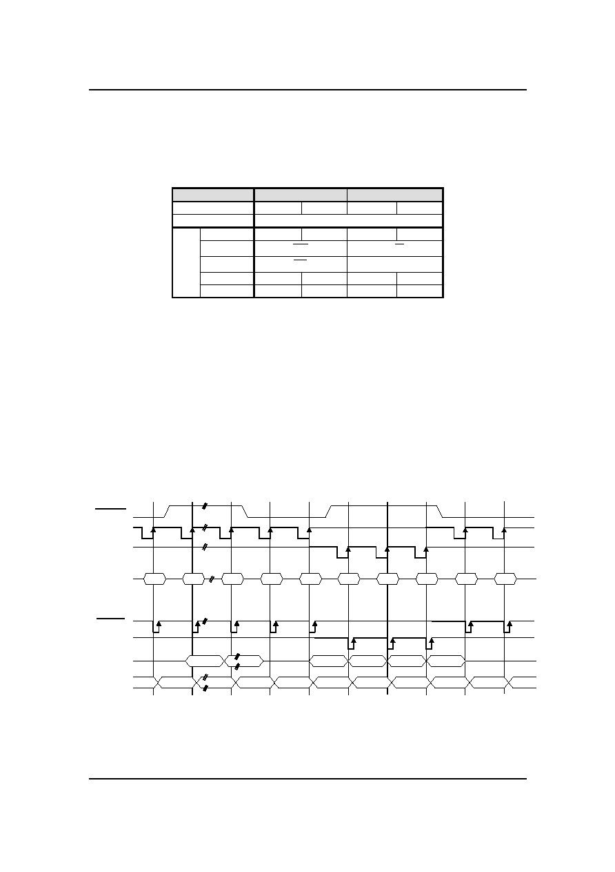
The timing relationship between UC1608 internal
control signal RD, WR and their associated bus
actions are shown in the figure below.
The Display RAM read interface is implemented
as a two-stage pipe-line. This architecture
requires that, every time memory address is
modified, either in 8-bit mode or 4-bit mode, by
either Set CA, or Set PA command, a dummy
read cycle need to be performed before the
actual data can propagate through the pipe-line
and be read from data port D[7:0].
There is no pipeline in write interface of Display
RAM. Data is transferred directly from bus buffer
to internal RAM on the rising edges of write
pulses.
8-
BIT
& 4-
BIT
B
US
O
PERATION
UC1608 supports both 8-bit and 4-bit bus width.
The bus width is determined by pin BM[1].
4-bit bus operation exactly doubles the clock
cycles of 8-bit bus operation, MSB followed by
LSB, including the dummy read, which also
requires two clock cycles.
L
LSB
D
L
D
L+K
C
MSB
C
LSB
Dummy
D
C
D
C+1
M
MSB
M
LSB
L
L+K
L+K+1
C
C+1
C+2
C+3
M
D
L
D
L+K
Dummy
D
C
D
C+1
D
C+2
External
CD
___
WR
__
RD
D[7:0]
Internal
Write
Read
Data
Latch
Column
Address
Figure 5: 8 bit Parallel Interface & Related Internal Signals

U
LTRA
C
HIP
High-Voltage Mixed-Signal IC
�1999-2002
20
Revision 0.52
D
ISPLAY
D
ATA
RAM
D
ATA
O
RGANIZATION
The display data is 1-bit per pixel and stored in a
dual port static RAM (RAM, for Display Data RAM).
The RAM size is 128x240 for UC1608. This array
of data bits is further organized into pages of 8 bit
slices to facilitate parallel bus interface.
When Mirror X (MX, LC[2]) is OFF, the 1
st
column
of LCD pixels will correspond to the bits of the first
byte of each page, the 2
nd
column of LCD pixels
correspond to the bits of the second byte of each
page, etc.
MSB F
IRST OR
LSB F
IRST
There are two options to map D[7:0] to RAM, MSB
first (MSF=1), or LSB first (MSF=0), as illustrated in
next page.
D
ISPLAY
D
ATA
RAM A
CCESS
The memory used in UC1608 Display Data RAM
(RAM) is a special purpose dual port RAM which
allows asynchronous access to both its column and
row data. Thus, RAM can be independently
accessed both for Host Interface and for display
operations.
D
ISPLAY
D
ATA
RAM A
DDRESSING
A Host Interface (HI) memory access operation
starts with specifying Page Address (PA) and
Column Address (CA) by issuing Set Page Address
and Set Column Address commands.
If wrap-around (WA, AC[0]) is OFF (0), CA will stop
increasing after reaching the end of page (239),
and system programmers need to set the values of
PA and CA explicitly.
If WA is ON (1), when CA reaches end of page, CA
will be reset to 0 and PA will increment or
decrement, depending on the setting of Page
Increment Direction (PID, AC[2]). When PA
reaches the boundary of RAM (i.e. PA = 0 or 19),
PA will be wrapped around to the other end of RAM
and continue.

UC1608
128x240 Matrix LCD Controller-Drivers
(Revision 0.52 Preview)
21
Line
0
1
Address
SL=0 SL=16 SL=0
SL=0 SL=16 SL=16
D0
D7
00H
COM1
COM113 COM128
COM96
COM16
---
D1
D6
01H
COM2
COM114 COM127
COM95
COM15
---
D2
D5
02H
COM3
COM115 COM126
COM94
COM14
---
D3
D4
03H
COM4
COM116 COM125
COM93
COM13
---
D4
D3
04H
COM5
COM117 COM124
COM92
COM12
---
D5
D2
05H
COM6
COM118 COM123
COM91
COM11
---
D6
D1
06H
COM7
COM19
COM122
COM90
COM10
---
D7
D0
07H
COM8
COM120 COM121
COM89
COM9
---
D0
D7
08H
COM9
COM121 COM120
COM88
COM8
---
D1
D6
09H
COM10
COM122 COM119
COM87
COM7
---
D2
D5
0AH
COM11
COM123 COM118
COM86
COM6
---
D3
D4
0BH
COM12
COM124 COM117
COM85
COM5
---
D4
D3
0CH
COM13
COM125 COM116
COM84
COM4
---
D5
D2
0DH
COM14
COM126 COM115
COM83
COM3
---
D6
D1
0EH
COM15
COM127 COM114
COM82
COM2
---
D7
D0
0FH
COM16
COM128 COM113
COM81
COM1
---
D0
D7
10H
COM17
COM1
COM112
COM80
COM128
---
D1
D6
11H
COM18
COM2
COM111
COM79
COM127
---
D2
D5
12H
COM19
COM3
COM110
COM78
COM126
---
D3
D4
13H
COM20
COM4
COM109
COM77
COM125
---
D4
D3
14H
COM21
COM5
COM108
COM76
COM124
---
D5
D2
15H
COM22
COM6
COM107
COM75
COM123
---
D6
D1
16H
COM23
COM7
COM106
COM74
COM122
---
D7
D0
17H
COM24
COM8
COM105
COM73
COM121
---
D0
D7
18H
COM25
COM9
COM104
COM72
COM120
COM96
D1
D6
19H
COM26
COM10
COM103
COM71
COM119
COM95
D2
D5
1AH
COM27
COM11
COM102
COM70
COM118
COM94
D3
D4
1BH
COM28
COM12
COM101
COM69
COM117
COM93
D4
D3
1CH
COM29
COM13
COM100
COM68
COM116
COM92
D5
D2
1DH
COM30
COM14
COM99
COM67
COM115
COM91
D6
D1
1EH
COM31
COM15
COM98
COM66
COM114
COM90
D7
D0
1FH
COM32
COM16
COM97
COM65
COM113
COM89
D0
D7
30H
COM113
COM97
COM16
---
COM32
---
D1
D6
31H
COM114
COM98
COM15
---
COM31
---
D2
D5
32H
COM115
COM99
COM14
---
COM30
---
D3
D4
33H
COM116 COM100
COM13
---
COM29
---
D4
D3
34H
COM117 COM101
COM12
---
COM28
---
D5
D2
35H
COM118 COM102
COM11
---
COM27
---
D6
D1
36H
COM19
COM103
COM10
---
COM26
---
D7
D0
37H
COM120 COM104
COM9
---
COM25
---
D0
D7
38H
COM121 COM105
COM8
---
COM24
---
D1
D6
39H
COM122 COM106
COM7
---
COM23
---
D2
D5
3AH
COM123 COM107
COM6
---
COM22
---
D3
D4
3BH
COM124 COM108
COM5
---
COM21
---
D4
D3
3CH
COM125 COM109
COM4
---
COM20
---
D5
D2
3DH
COM126 COM110
COM3
---
COM19
---
D6
D1
3EH
COM127 COM111
COM2
---
COM18
---
D7
D0
3FH
COM128 COM112
COM1
---
COM17
---
128
96
128
96
0
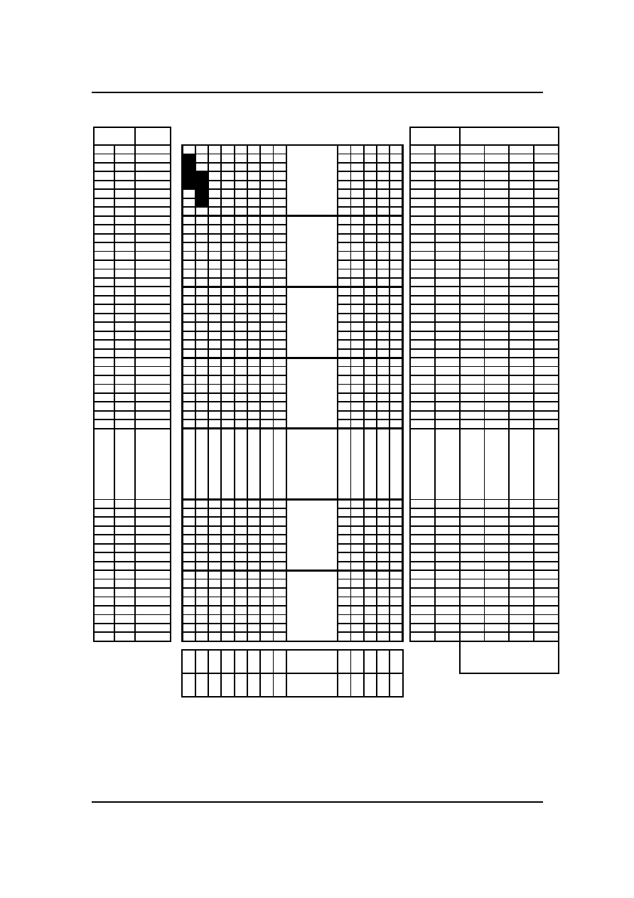
SEG1
SEG2
SEG3
SEG4
SEG5
SEG6
SEG7
SEG8
SEG236
SEG237
SEG238
SEG239
SEG240
1
SEG240
SEG239
SEG238
SEG237
SEG236
SEG235
SEG234
SEG233
SEG5
SEG4
SEG3
SEG2
SEG1
MSF
Page 1
Page 2
Page 3
MX
MY=1
Page 15
Page 14
MY=0
MUX
Page 0
Example for memory mapping: let MX = 0, MY = 0, SL = 0, MSF = 0, according to the data shown in the
above table:
Page 0 SEG 1: 00011110b
Page 0 SEG 2: 01111000b

U
LTRA
C
HIP
High-Voltage Mixed-Signal IC
�1999-2002
22
Revision 0.52
MX I
MPLEMENTATION
Column Mirroring (MX) is implemented by selecting
either (CA) or (239�CA) as the RAM column
address. Changing MX affects the data written to
the RAM.
Since MX has no effect on data already stored in
RAM, changing MX does not have immediate effect
on the displayed pattern. To refresh the display,
refresh the data stored in RAM after setting MX.
D
ISPLAY
S
CANNING
During each field of display, depending on the
setting of MR, COM electrodes will be scanned in a
fixed pattern at a rate of
(Frame Rate x Mux Rate) rows/second.
During each row period, the signal at the SEG
drivers determines the ON/OFF status of the row of
pixels being scanned.
R
OW
S
CANNING
For each field, the scanning starts at COM1
through COMx, where x depends on the setting of
MR.
COM electrode scanning (row scanning) orders are
not affected by Start Line (SL) or Mirror Y (MY,
LC[3]). When MY is 0, the effect of SL having a
value K is to change the mapping of COM1 to the
K-th bit slice of data stored in display RAM. Visually,
SL having a non-zero value is equivalent to
scrolling LCD display up by SL rows.
RAM A
DDRESS
G
ENERATION
The mapping of the data stored in the display
SRAM and the scanning electrodes can be
obtained by combining the fixed Row scanning
sequence and the following RAM address
generation formula.
During the display operation, the RAM line address
generation can be mathematically represented as
following:
For the 1
st
line period of each field
Line = SL
Otherwise
Line = Mod(Line+1, 128)
Where Mod is the modular operator, and Line is the
bit slice line address of RAM to be outputted to
SEG drivers. Line 0 corresponds to the first bit-slice
of data in RAM.
The above Line generation formula produces the
"loop around" effect as it effectively resets Line to 0
when Line+1 reaches 128.
Effects such as page scrolling can be emulated by
changing SL dynamically.
MY I
MPLEMENTATION
Row Mirroring (MY) is implemented by reversing
the mapping order between COM electrodes and
RAM, i.e. the mathematical address generation
formula becomes:
For the 1
st
line period of each field
Line = Mod(SL + MUX-1, 128)
where MUX = 96 or 128.
Otherwise
Line = Mod(Line-1 , 128)
Visually, the effect of MY is equivalent to flipping
the display upside down. The data stored in display
RAM is not affected by MY.

UC1608
128x240 Matrix LCD Controller-Drivers
(Revision 0.52 Preview)
23
R
ESET
& P
OWER
M
ANAGEMENT
T
YPES OF
R
ESET
UC1608 has two different types of Reset:
Power-ON-Reset and System-Reset.
Power-ON-Reset is performed right after V
DD
is
connected to power. Power-On-Reset will first wait
for about ~15mS, depending on the time required
for V
DD
to stabilize, and then trigger the System
Reset.
System Reset can also be activated by software
command or by connecting RST pin to ground. In
the following discussions, Reset means System
Reset.
R
ESET
S
TATUS
When UC1608 enters RESET sequence:
�
Operation mode will be "Reset"
�
System Status bits RS and BZ will stay as "1"
until the Reset process is completed. When
RS=1, the IC will only respond to Read Status
command. All other commands are ignored.
�
All control registers are reset to default values.
Refer to Control Registers for details of their
default values.
O
PERATION
M
ODES
UC1608 has three operating modes (OM):
Reset, Normal, Sleep.
Mode
Reset
Sleep Normal
OM 00
10
11
Host Interface
Active
Active Active
Clock
OFF OFF ON
LCD
Drivers OFF OFF ON
Charge
Pump OFF OFF ON
Draining Circuit
ON
OFF
OFF
Table 11: Operating Modes
C
HANGING
O
PERATION
M
ODE
In addition to Power-ON-Reset, two commands will
initiate OM transitions:
Set Display Enable, and System Reset.
When DC[2] is modified by Set Display Enable, OM
will be updated automatically. There is no other
action required to enter Sleep mode.
For maximum energy utilization, Sleep mode is
designed to retain charges stored in external
capacitors C
B0
, C
B1
, and C
L
. To drain these
capacitors, use Reset command to activate the on-
chip draining circuit.
Action
Mode
OM
Set Driver Enable to "0"
Sleep
10
Set Driver Enable to "1"
Normal
11
Reset command or
RST_ pin pulled "L"
Power ON reset
Reset 00
Table 12: OM changes
Even though UC1608 consumes very little energy
in Sleep mode (typically 5uA or less), however,
since all capacitors are still charged, the leakage
through COM drivers may damage the LCD over
the long term. It is therefore recommended to use
Sleep mode only for brief Display OFF operations,
such as full-frame screen updates, and to use
RESET for extended screen OFF operations.
E
XITING
S
LEEP
M
ODE
UC1608 contains internal logic to check whether
V
LCD
and V
BIAS
are ready before releasing COM
and SEG drivers from their idle states. When
exiting Sleep or Reset Mode, COM and SEG
drivers will not be activated until UC1608 internal
voltage sources are restored to their proper values.

U
LTRA
C
HIP
High-Voltage Mixed-Signal IC
�1999-2002
24
Revision 0.52
P
OWER
-U
P
S
EQUENCE
UC1608 power-up sequence is simplified by built-in
"Power Ready" flags and the automatic invocation
of System-Reset command after Power-ON-Reset.
System programmers are only required to wait 15~
20 ms before the CPU starting to issue commands
to UC1608. No additional time sequences are
required between enabling the charge pump,
turning on the display drivers, writing to RAM or
any other commands.
P
OWER
-D
OWN
S
EQUENCE
To prevent the charge stored in capacitors C
BX+
,
C
BX�
, and C
L
from damaging the LCD when V
DD
is
switched off, use Reset mode to enable the built-in
draining circuit and discharge these capacitors.
The draining resistor is 1K Ohm for both V
LCD
and
V
B+
. It is recommended to wait 3 x RC for V
LCD
and
1.5 x RC for V
B+
. For example, if C
L
is 10nF, then
the draining time required for V
LCD
is 1~2mS.
When internal V
LCD
is not used, UC1608 will NOT
drain V
LCD
during RESET. System designers need
to make sure external V
LCD
source is properly
drained off before turning off V
DD
.
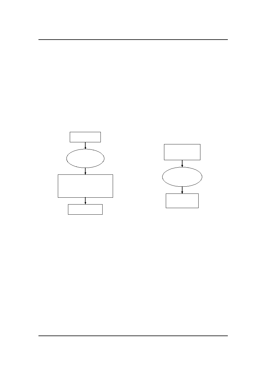
Turn on VDD
Set LCD Bias Ratio (BR)
Set Gain (GN)
Set Potential Meter (PM)
Set Display Enable
Wait 15~20 mS
Figure 12: Reference Power-Up Sequence
Turn off VDD
Reset command
Wait 1~2 mS
Figure 13: Reference Power-Down Sequence

UC1608
128x240 Matrix LCD Controller-Drivers
(Revision 0.52 Preview)
25
S
AMPLE
P
OWER
C
OMMAND
S
EQUENCES
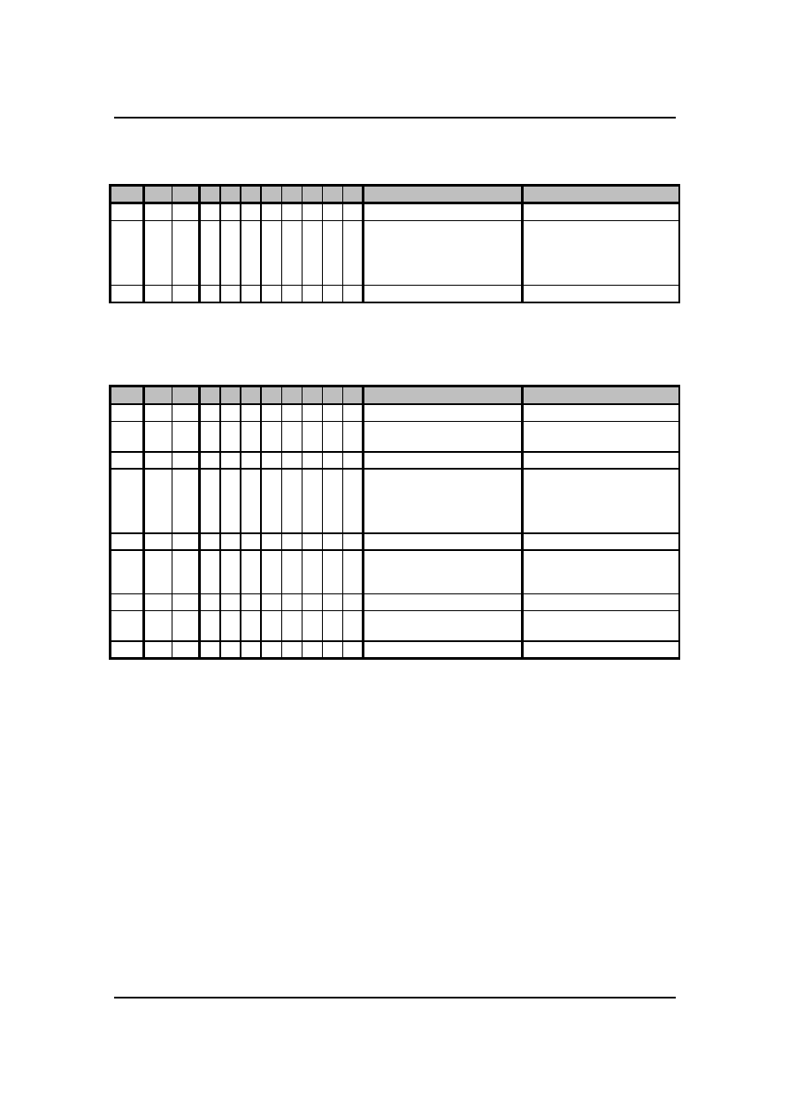
The following tables are examples of command sequence for power-up, power-down and display ON/OFF
operations. These are only to demonstrate some "typical, generic" scenarios. Designers are encouraged to
study related sections of the datasheet and find out what the best parameters and control sequences are for
their specific design needs.
C/D
The type of the interface cycle. It can be either Command (0) or Data (1)
W/R
The direction of data flow of the cycle. It can be either Write (0) or Read (1).
Type Required: These items are required
Customer: These item are not necessary if customer parameters are the same as default
Advanced: We recommend new users to skip these commands and use default values.
Optional: These commands depend on what users want to do.
P
OWER
-U
P
Type C/D W/R D7 D6 D5 D4 D3 D2 D1 D0
Chip action
Comments
R � � � � � � � � � � Automatic
Power-ON-Reset. Wait
~20ms
after
V
DD
is ON
C 0 0 0 0 1 0 0 # # # (5)
Set
MR
and
TC
C 0 0 1 1 0 0 # # # # (15)
Set
LCD
Mapping
Set up LCD specific
parameters such as format,
MX, MY, MSF, etc.
C 0 0 1 1 1 0 1 0 # # (18)
Set
Bias
Ratio
R
0
0
0
0
1
#
0
#
0
#
0
#
0
#
0
#
0
#
1
#
(9) Set Gain & PM
C 1
.
.
1
0
.
.
0
#
.
.
#
#
.
.
#
#
.
.
#
#
.
.
#
#
.
.
#
#
.
.
#
#
.
.
#
#
.
.
#
Write display RAM
Set up display image
R 0 0 1 0 1 0 1 1 1 1 (13)
Set
Display
Enable
P
OWER
-D
OWN
Type C/D W/R D7 D6 D5 D4 D3 D2 D1 D0
Chip action
Comments
R 0 0 1 1 1 0 0 0 1 0 (16)
System
Reset
R � � � � � � � � � � Draining
capacitor
Wait
1~2ms
before
V
DD
OFF

U
LTRA
C
HIP
High-Voltage Mixed-Signal IC
�1999~2002
26
B
RIEF
D
ISPLAY
-OFF
Type C/D W/R D7 D6 D5 D4 D3 D2 D1 D0
Chip action
Comments
R 0 0 1 0 1 0 1 1 1 0 (13)
Set
Display
Disable
C 1
.
.
1
0
.
.
0
#
.
.
#
#
.
.
#
#
.
.
#
#
.
.
#
#
.
.
#
#
.
.
#
#
.
.
#
#
.
.
#
Write display RAM
Set up display image (Image
update is optional. Data in
the RAM is retained through
the SLEEP state.)
R 0 0 1 0 1 0 1 1 1 1 (13)
Set
Display
Enable
* This is only recommended for very brief display OFF (under 10mS).
If image becomes unstable use the Extended Display OFF approach shown below.
E
XTENDED
D
ISPLAY
-OFF
Type C/D W/R D7 D6 D5 D4 D3 D2 D1 D0
Chip action
Comments
R 0 0 1 1 1 0 0 0 1 0 (16)System
Reset.
C
B1
, C
B1
, C
LCD
discharged.
� � � � � � � � � � �
Extended display OFF
Z z z z . . .
� � � � � � � � � � �
System
waking
up
C 1
.
.
1
0
.
.
0
#
.
.
#
#
.
.
#
#
.
.
#
#
.
.
#
#
.
.
#
#
.
.
#
#
.
.
#
#
.
.
#
Write display RAM
Set up display image (Image
update is optional. Data in
the RAM is retained through
the RESET state.)
C 0 0 0 0 1 0 0 # # # (5)
Set
MR
and
TC
C 0 0 1 1 0 0 # # # # (15)
Set
LCD
Mapping
Set up LCD specific
parameters such as format,
MX, MY, MSF, etc.
C 0 0 1 1 1 0 1 0 # # (18)
Set
Bias
Ratio
C
0
0
0
0
1
#
0
#
0
#
0
#
0
#
0
#
0
#
1
#
(9) Set Gain & PM
R 0 0 1 0 1 0 1 1 1 1 (13)
Set
Display
Disable
* The sequence is basically the same as the power up sequence, except Power-ON RESET is replaced by
System RESET command, and an extended idle time in between.

UC1608
128x240 Matrix LCD Controller-Drivers
(Revision 0.52 Preview)
27
A
BSOLUTE
M
AXIMUM
R
ATINGS
In accordance with IEC134, note 1,2 and 3.
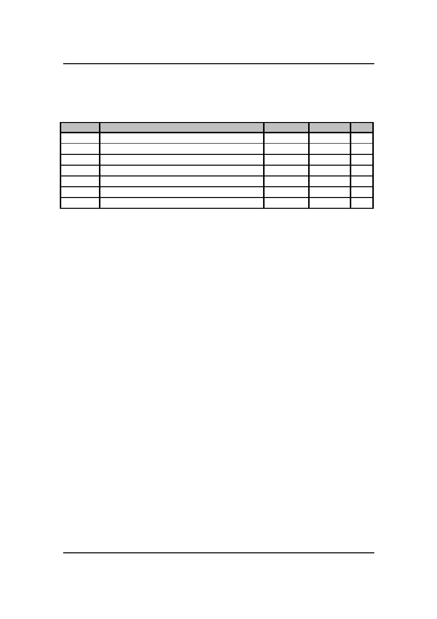
Symbol
Parameter
Min.
Max.
Unit
V
DD
Logic
Supply
voltage
-0.3
+4.0 V
V
DD2
LCD Generator Supply voltage
-0.3
+4.0
V
V
DD3
Analog Circuit Supply voltage
-0.3
+4.0
V
V
LCD
LCD Generated voltage (-30
O
C ~ +80
O
C) -0.3
+17.0
V
V
IN
Any input voltage
-0.4
V
DD
+ 0.5
V
T
OPR
Operating
temperature
range
-30
+85
o
C
T
STR
Storage
temperature
-55
+125
o
C
Notes
1. V
DD
based on V
SS
= 0V
2. Stress values listed above may cause permanent damages to the device.

U
LTRA
C
HIP
High-Voltage Mixed-Signal IC
�1999~2002
28
S
PECIFICATIONS
DC C
HARACTERISTICS
Symbol
Parameter
Conditions
Min.
Typ.
Max.
Unit
V
DD
Supply for digital circuit
2.4
2.8
3.6
V
V
DD2/3
Supply for bias & pump
2.4
2.8
3.6
V
V
LCD
Charge
pump
output
V
DD2/3
>= 2.4V, 25
O
C
12.5
15
V
V
D
LCD
data
voltage
V
DD2/3
>= 2.4V, 25
O
C
1.2
V
V
IL
Input logic LOW
0.2V
DD
V
V
IH
Input logic HIGH
0.8V
DD
V
V
OL
Output logic LOW
0.2V
DD
V
V
OH
Output logic HIGH
0.8V
DD
V
I
IL
Input leakage current
1.5
�A
C
IN
Input
capacitance
5
10 PF
C
OUT
Output
capacitance
5
10 PF
R
0(SEG)
SEG output impedance
V
LCD
= 12.5V
1.5
3
k
R
0(COM)
COM output impedance
V
LCD
= 12.5V
1.5
3
k
f
LINE
Average frame rate
90
Hz

UC1608
128x240 Matrix LCD Controller-Drivers
(Revision 0.52 Preview)
29
AC C
HARACTERISTICS
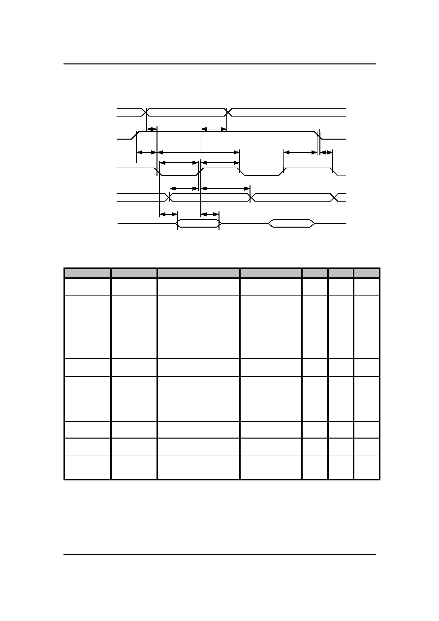
Figure 21: Parallel Bus Timing Characteristics (for 8080 MCU)
(VDD=2.4V to 3.3V, Ta= �30 to +85
o
C)
Symbol
Signal
Description
Condition
Min.
Max.
Units
t
AS80
t
AH80
CD
Address setup time
Address hold time
0
10
� ns
t
CY80
System cycle time
8 bits bus (read)
(write)
4 bits bus (read)
(write)
140
140
80
80
� ns
t
PWR80
WR1
Pulse width 8 bits (read)
4 bits
65
35
� ns
t
PWW80
WR0
Pulse width 8 bits (write)
4 bits
65
35
� ns
t
HPW80
WR0, WR1
High pulse width
8 bits bus (read)
(write)
4 bits bus (read)
(write)
65
65
35
35
� ns
t
DS80
t
DH80
D0~D7
Data setup time
Data hold time
30
10
� ns
t
ACC80
t
OD80
Read access time
Output disable time
C
L
= 100pF
�
10
50
50
ns
t
CSSA80
t
CSSD80
t
CSH80
CS
Chip select setup time
10
10
20
ns
CD
t
AS80
t
AH80
CS
t
CSSA80
t
CY80
t
CSH80
t
CSSD80
t
PWR80
, t
PWW80
t
HPW80
WR0
t
DS80
t
DH80
Write
D[X]
t
ACC80
t
OD80
Read
D[X]

U
LTRA
C
HIP
High-Voltage Mixed-Signal IC
�1999~2002
30
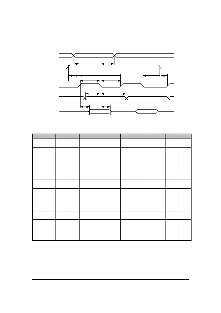
Figure 22: Parallel Bus Timing Characteristics (for 6800 MCU)
(VDD=2.4V to 3.3V, Ta= �30 to +85
o
C)
Symbol
Signal
Description
Condition
Min.
Max.
Units
t
AS68
t
AH68
CD
Address setup time
Address hold time
0
10
� ns
t
CY68
System cycle time
8 bits bus (read)
(write)
4 bits bus (read)
(write)
140
140
80
80
� ns
t
PWR68
WR1
Pulse width 8 bits (read)
4 bits
65
35
� ns
t
PWW68
Pulse width 8 bits (write)
4 bits
65
35
� ns
t
LPW68
Low pulse width
8 bits bus (read)
(write)
4 bits bus (read)
(write)
65
65
35
35
� ns
t
DS68
t
DH68
D0~D7
Data setup time
Data hold time
30
10
� ns
t
ACC68
t
OD68
Read access time
Output disable time
C
L
= 100pF
�
10
50
50
ns
T
CSSA68
T
CSSD68
T
CSH68
CS
Chip select setup time
10
10
20
ns
CD
t
AS68
t
AH68
CS
t
CSSA68
t
CY68
t
CSH68
t
CSSD68
t
PWR68
, t
PWW68
t
LPW68
WR0
t
DS68
t
DH68
Write
D[7:0]
t
ACC68
t
OD68
Read
D[7:0]

UC1608
128x240 Matrix LCD Controller-Drivers
(Revision 0.52 Preview)
31
RST
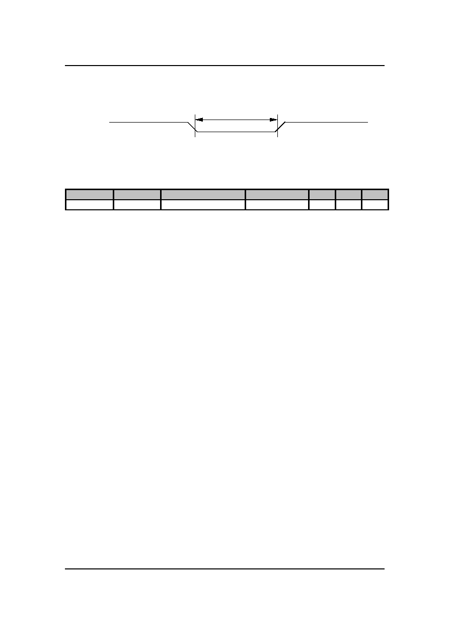
t
RW
Figure 25: Reset Characteristics
(VDD=2.4V to 3.3V, Ta= �30 to +85
o
C)
Symbol
Signal
Description
Condition
Min.
Max.
Units
t
RW
RST
Reset low pulse width
1000
�
ns

U
LTRA
C
HIP
High-Voltage Mixed-Signal IC
�1999~2002
32
P
HYSICAL
D
IMENSIONS
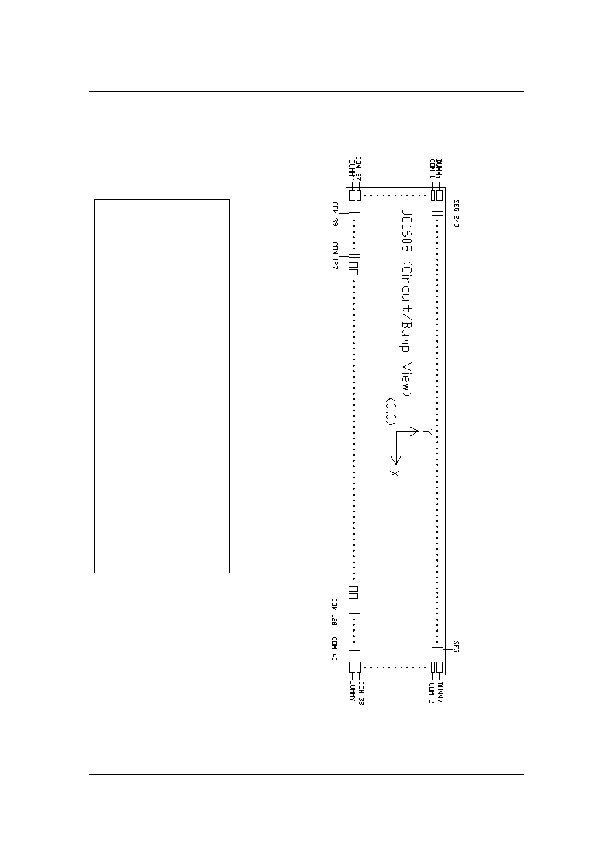
C
HIP SIZE
12.603
X
1.248mm
D
IE
T
HICKNESS
:
0.5mm
A
U
B
UMP HEIGHT
:
17m �1m (within die)
AU B
UMP PITCH
:
50m
A
U
B
UMP SIZE
:
94 x 32m
94 x 51m
106 x 48m
D
UMMY
B
UMP SIZE
:
94 x 57m
106 x 48m
P
AD COORDINATES
:
Pad center
P
AD ORIGIN
:
Chip center
(Drawing and coordinates are
for the Circuit/Bump view.)

UC1608
128x240 Matrix LCD Controller-Drivers
(Revision 0.52 Preview)
33
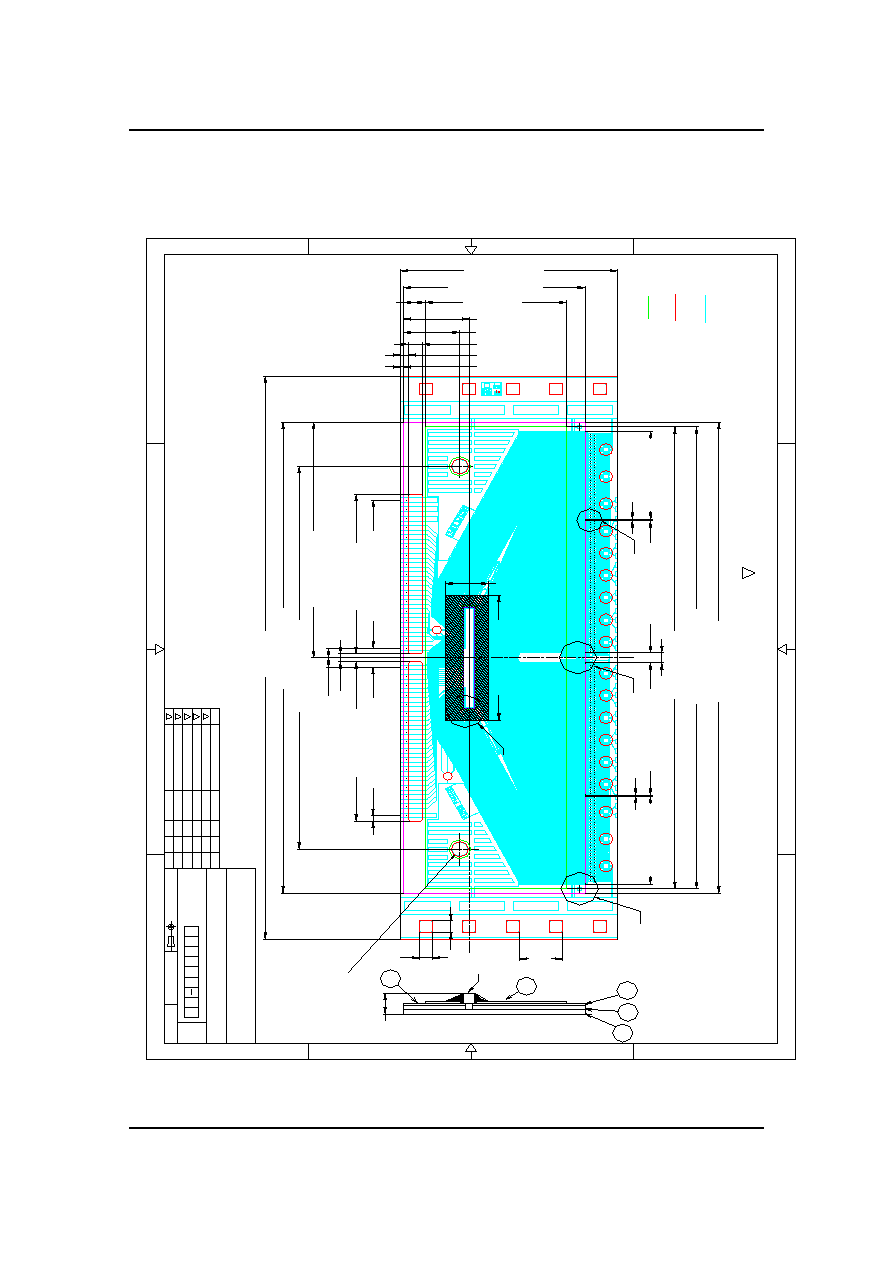
COF I
NFORMATION
U
N
I
T
S
H
O
W
N F
R
O
M
C
O
PP
ER
SI
DE
SO
L
D
ER
RES
I
S
T
ME
T
A
L
(
C
u
)
PO
L
Y
I
M
I
D
E
TST4
BM0
BM1
RST
NC
CS
D7
D6
D5
D4
D3
D2
D0
W R1
CD
W R0
D1
VSS
VDD
VLCD
VDD2,3
VB2+
VB1-
VB1+
VB0-
VB0+
VB2-
NC
NC
NC
NC
NC
VB3-
VB3+
4
3
2
4
1
C
LT
R
A
U
IN
C
.
HI
P
,W
=
0
.
0
7
CL
CL
(
I
ncl
ude I
C
)
,
W
=
0
.
0
7
,
W
=
0.
088
,W
=
0
.
0
8
8
1
34
1
372
2
PRO
J
ECT
I
ON
DR
A
W
I
N
G NO.
U
C
1608 C
O
F
P
a
ck
a
g
e
D
r
aw
i
n
g
SCAL
E 1
:
1
TI
TL
E
U
C
6
1
08
S
H
T
2 of
2
FA
REV
1
2
3
4
5
Re
v
i
s
e
De
s
c
r
i
b
t
i
o
n
D
F
T
G
.
CHK
.
A
P
P
V
L
.
Da
t
e
Ne
w v
e
r
s
i
o
n
06/
11/
20
02
J
a
c
k
Al
v
i
n
M
o
di
f
i
ed t
he t
e
x
t
c
o
m
m
ent
06/
18/
20
02
J
a
c
k
Al
v
i
n
Adde
d N
o
t
e
9
.
2
2
A
B
C
D
3
C
1
A
B
C
D
4
B
D
2
A
1
43
IC
0.
8 M
A
X
.
0.914
1.5 (PI window)
0.362
2.353
4.73 (Resin area)
15.
5
6 (
R
es
i
n
ar
ea
)
"C
"
0.
7
2.
4
58.
53
�
0.
2 (
C
ut
-
l
i
n
e)
1.
27
"D
"
1.
42
1.42
4.75
"B
"
"A
"
2-
?1.
800
2
9
.
2
6
5
(
I
C
Ce
n
t
e
r
)
1
47.
6
(
A
l
i
g
n
m
e
nt
H
o
l
e
)
19.
8(
P
I
W
i
n
d
o
w
)
P
1
.
1
5x16
=18.
4,
W
=
0.
6
1
9
.8
(P
I W
i
n
d
o
w
)
P
1
.
1
5x16
=18.
4,
W
=
0.
6
15.497 (S/R)
19.85� 0.2 (Cut-line)
6.152 (Alignm ent hole)
7.188 (IC center)
57.
39
�
0.
2
(
S
/
R
)
58.
53
�
0.
2 (
C
ut
-
l
i
n
e)
57.
3
9 (
A
l
i
gnm
ent
m
a
r
k
)
0.
168
P
0
.
1
68x6
5=10.
9
2
P
0
.
138x1
19=1
6
.
4
22
P
0
.
1
38x1
19=1
6
.
4
22
0.
168
P
0
.
168x6
5=10.
92
69.
95
�
0.
12
5S.Px4.75=23.75

U
LTRA
C
HIP
High-Voltage Mixed-Signal IC
�1999~2002
34
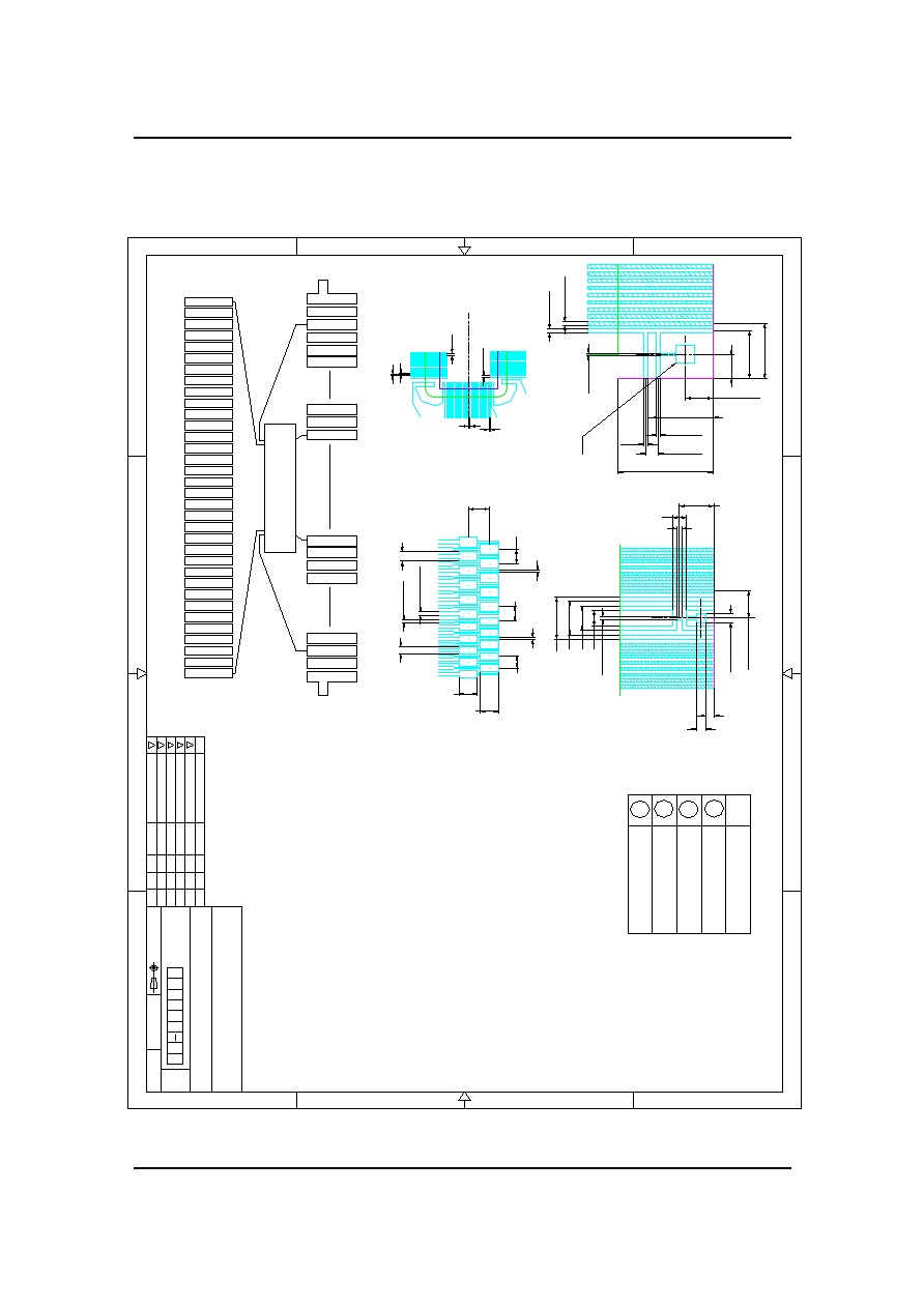
COF I
NFORMATION
B
a
s
e
F
ilm
C
oppe
r
S
o
l
d
e
r
R
e
si
st
P
l
at
i
n
g
2
3
4
No
.
1
Ma
t
e
r
i
a
l
C
o
m
ponent
L
i
s
t
Com1
NC
Com5
Com3
Com125
Com127
NC
NC
Com2
Com4
Com122
Com124
NC
Com126
Com128
Seg240
Seg1
D2
D1
D0
W R1
W R0
CD
RST
TST4
CS
BM0
BM1
NC
U
C
1608
I
C
VB3-
VB3+
VB2-
VB2+
VB1-
VB1+
VB0-
VB0+
VLCD
VDD2,3
NC
NC
NC
VSS
VDD
NC
NC
D7
D6
D5
D4
D3
De
t
a
i
l
"
A
"
2
2
A
B
C
D
3
C
1
A
4
B
C
D
4
3
PR
O
J
EC
T
I
O
N
DRAW
I
NG
NO
.
U
C
1
6
0
8
C
O
F P
a
c
k
ag
e
D
r
aw
i
n
g
SC
AL
E
1
:
1
TI
T
L
E
U
C
6
1
08
SH
T
1
o
f
2
FA
REV
A
B
C
LTR
A
U
IN
C
.
HI
P
1
2
3
4
5
Re
v
i
s
e
De
s
c
r
i
b
t
i
o
n
DF
T
G
.
CHK
.
A
P
P
V
L
.
Da
t
e
Ne
w v
e
r
s
i
o
n
0
6
/
1
1
/
2
0
0
2
Ja
ck
A
l
vi
n
D
1
De
t
a
i
l
"
B
"
D
e
t
a
i
l
"
C
"
D
et
ai
l
"
D
"
CL
0.
07
0.
088
0.
06
0.
635
0.
2048
0.
06
0.
57
0.45
0.
336
0.
045
0.
035
0.
175
0.
225
0.3857
0.
276
0.
336
0.025
0.025
0.
044
0
.
050(
P
i
t
c
h)
0
.
025(
S
pace)
0
.
025
(
W
i
d
t
h
)
0.
983
0.
783
0.
579
0.
379
0.3024
0.7354
0.1024
0.2408
0.1722
0.
4 S
Q
0.
09
0.
088
1.
288
1.
12
0.09
0.27
0.09
1.155
0.585
1
372
2
0.3857
M
o
di
f
i
ed
t
h
e
t
e
x
t
c
o
m
m
ent
06
/
1
8
/
2
002
J
a
c
k
Al
v
i
n
A
d
de
d N
o
t
e
9.
1
34
2
UN
I
T
S
H
OW
N F
R
OM
COP
P
E
R
S
I
D
E

UC1608
128x240 Matrix LCD Controller-Drivers
(Revision 0.52 Preview)
35
P
AD
C
OORDINATES
Pin
Name
X
Y
W
H
1 Dummy -6185.5
-509.5 94 57
2 COM37 -6185.5
-450.0 94 32
3 COM35 -6185.5
-400.0 94 32
4 COM33 -6185.5
-350.0 94 32
5 COM31 -6185.5
-300.0 94 32
6 COM29 -6185.5
-250.0 94 32
7 COM27 -6185.5
-200.0 94 32
8 COM25 -6185.5
-150.0 94 32
9 COM23 -6185.5
-100.0 94 32
10 COM21 -6185.5 -50.0 94 32
11 COM19 -6185.5 0.0 94 32
12 COM17 -6185.5 50.0 94 32
13 COM15 -6185.5 100.0 94 32
14 COM13 -6185.5 150.0 94 32
15 COM11 -6185.5 200.0 94 32
16 COM9 -6185.5
250.0 94 32
17 COM7 -6185.5
300.0 94 32
18 COM5 -6185.5
350.0 94 32
19 COM3 -6185.5
400.0 94 32
20 COM1 -6185.5
450.0 94 32
21
Dummy -6185.5 509.5 94 57
22 COM39 -6006.1
-521.0 51 94
23 COM41 -5946.6
-521.0 32 94
24 COM43 -5896.6
-521.0 32 94
25 COM45 -5846.6
-521.0 32 94
26 COM47 -5796.6
-521.0 32 94
27 COM49 -5746.6
-521.0 32 94
28 COM51 -5696.6
-521.0 32 94
29 COM53 -5646.6
-521.0 32 94
30 COM55 -5596.6
-521.0 32 94
31 COM57 -5546.6
-521.0 32 94
32 COM59 -5496.6
-521.0 32 94
33 COM61 -5446.6
-521.0 32 94
34 COM63 -5396.6
-521.0 32 94
35 COM65 -5346.6
-521.0 32 94
36 COM67 -5296.6
-521.0 32 94
37 COM69 -5246.6
-521.0 32 94
38 COM71 -5196.6
-521.0 32 94
39 COM73 -5146.6
-521.0 32 94
40 COM75 -5096.6
-521.0 32 94
41 COM77 -5046.6
-521.0 32 94
42 COM79 -4996.6
-521.0 32 94
43 COM81 -4946.6
-521.0 32 94
44 COM83 -4896.6
-521.0 32 94
45 COM85 -4846.6
-521.0 32 94
46 COM87 -4796.6
-521.0 32 94
Pin
Name
X
Y
W
H
47 COM89 -4746.6
-521.0 32 94
48 COM91 -4696.6
-521.0 32 94
49 COM93 -4646.6
-521.0 32 94
50 COM95 -4596.6
-521.0 32 94
51 COM97 -4546.6
-521.0 32 94
52 COM99 -4496.6
-521.0 32 94
53 COM101 -4446.6 -521.0 32 94
54 COM103 -4396.6 -521.0 32 94
55 COM105 -4346.6 -521.0 32 94
56 COM107 -4296.6 -521.0 32 94
57 COM109 -4246.6 -521.0 32 94
58 COM111 -4196.6 -521.0 32 94
59 COM113 -4146.6 -521.0 32 94
60 COM115 -4096.6 -521.0 32 94
61 COM117 -4046.6 -521.0 32 94
62 COM119 -3996.6 -521.0 32 94
63 COM121 -3946.6 -521.0 32 94
64 COM123 -3896.6 -521.0 32 94
65 COM125 -3846.6 -521.0 32 94
66 COM127 -3796.6 -521.0 32 94
67 TST2 -3746.6
-521.0
32 94
68 TST3 -3687.1
-521.0
51 94
69 Dummy -3351.9
-544.0 106 48
70 Dummy -3226.9
-544.0 106 48
71 Dummy -3102.0
-544.0 106 48
72 Dummy -2977.0
-544.0 106 48
73 Dummy -2852.0
-544.0 106 48
74 Dummy -2727.0
-544.0 106 48
75 Dummy -2602.1
-544.0 106 48
76 Dummy -2477.1
-544.0 106 48
77 Dummy -2352.1
-544.0 106 48
78 Dummy -2227.1
-544.0 106 48
79 Dummy -2102.2
-544.0 106 48
80 Dummy -1977.2
-544.0 106 48
81 Dummy -1852.2
-544.0 106 48
82 Dummy -1727.2
-544.0 106 48
83 Dummy -1602.3
-544.0 106 48
84 Dummy -1477.3
-544.0 106 48
85 Dummy -1352.3
-544.0 106 48
86 Dummy -1227.3
-544.0 106 48
87 Dummy -1102.4
-544.0 106 48
88 Dummy -977.4 -544.0 106 48
89 Dummy -852.4 -544.0 106 48
90 Dummy -727.4 -544.0 106 48
91 Dummy -602.5 -544.0 106 48
92 Dummy -477.5 -544.0 106 48

U
LTRA
C
HIP
High-Voltage Mixed-Signal IC
�1999~2002
36
Product Specifications
Pin
Name
X
Y
W
H
93 Dummy -352.5 -544.0 106 48
94 Dummy -227.5 -544.0 106 48
95 Dummy -102.6 -544.0 106 48
96 Dummy 22.4 -544.0 106 48
97 Dummy 147.4 -544.0 106 48
98 Dummy 272.4 -544.0 106 48
99 Dummy 397.4 -544.0 106 48
100 BM1 1198.7
-515.0
48 106
101 BM0 1268.7
-515.0
48 106
102 CS 1338.7
-515.0
48
106
103 TST4 1408.7
-515.0 48 106
104 RST 1478.7
-515.0
48 106
105 CD 1548.7
-515.0
48
106
106 WR0 1618.7
-515.0 48 106
107 WR1 1688.7
-515.0 48 106
108 D0 1758.7
-515.0
48
106
109 D1 1828.7
-515.0
48
106
110 D2 1898.7
-515.0
48
106
111 D3 1968.7
-515.0
48
106
112 D4 2038.7
-515.0
48
106
113 D5 2108.7
-515.0
48
106
114 D6 2178.7
-515.0
48
106
115 D7 2248.7
-515.0
48
106
116 VDD 2342.0
-515.0
48 106
117 VDD2 2412.0 -515.0 48 106
118 VDD3 2482.0 -515.0 48 106
119 VSS2 2552.0
-515.0 48 106
120 VSS 2622.0
-515.0
48 106
121 TP1 2696.7
-521.0
32 94
122 TP2 2746.7
-521.0
32 94
123 TP3 2796.7
-521.0
32 94
124 VLCDOUT 2846.7 -521.0 32 94
125 VLCDIN 2896.7 -521.0 32 94
126 TST1 2946.7
-521.0 32 94
127 VB0+ 2996.7
-521.0 32 94
128 SB0+ 3046.7
-521.0 32 94
129 VB0- 3096.7
-521.0 32 94
130 SB0- 3146.7
-521.0 32 94
131 VB1+ 3196.7
-521.0 32 94
132 SB1+ 3246.7
-521.0 32 94
133 VB1- 3296.7
-521.0 32 94
134 SB1- 3346.7
-521.0 32 94
135 VB2+ 3396.7
-521.0 32 94
136 SB2+ 3446.7
-521.0 32 94
137 VB2- 3496.7
-521.0 32 94
138 SB2- 3546.7
-521.0 32 94
139 VB3+ 3596.7
-521.0 32 94
140 SB3+ 3646.7
-521.0 32 94
Pin
Name
X
Y
W
H
141 VB3- 3696.7
-521.0 32 94
142 SB3- 3746.7
-521.0 32 94
143 COM128 3796.7 -521.0 32 94
144 COM126 3846.7 -521.0 32 94
145 COM124 3896.7 -521.0 32 94
146 COM122 3946.7 -521.0 32 94
147 COM120 3996.7 -521.0 32 94
148 COM118 4046.7 -521.0 32 94
149 COM116 4096.7 -521.0 32 94
150 COM114 4146.7 -521.0 32 94
151 COM112 4196.7 -521.0 32 94
152 COM110 4246.7 -521.0 32 94
153 COM108 4296.7 -521.0 32 94
154 COM106 4346.7 -521.0 32 94
155 COM104 4396.7 -521.0 32 94
156 COM102 4446.7 -521.0 32 94
157 COM100 4496.7 -521.0 32 94
158 COM98 4546.7 -521.0 32 94
159 COM96 4596.7 -521.0 32 94
160 COM94 4646.7 -521.0 32 94
161 COM92 4696.7 -521.0 32 94
162 COM90 4746.7 -521.0 32 94
163 COM88 4796.7 -521.0 32 94
164 COM86 4846.7 -521.0 32 94
165 COM84 4896.7 -521.0 32 94
166 COM82 4946.7 -521.0 32 94
167 COM80 4996.7 -521.0 32 94
168 COM78 5046.7 -521.0 32 94
169 COM76 5096.7 -521.0 32 94
170 COM74 5146.7 -521.0 32 94
171 COM72 5196.7 -521.0 32 94
172 COM70 5246.7 -521.0 32 94
173 COM68 5296.7 -521.0 32 94
174 COM66 5346.7 -521.0 32 94
175 COM64 5396.7 -521.0 32 94
176 COM62 5446.7 -521.0 32 94
177 COM60 5496.7 -521.0 32 94
178 COM58 5546.7 -521.0 32 94
179 COM56 5596.7 -521.0 32 94
180 COM54 5646.7 -521.0 32 94
181 COM52 5696.7 -521.0 32 94
182 COM50 5746.7 -521.0 32 94
183 COM48 5796.7 -521.0 32 94
184 COM46 5846.7 -521.0 32 94
185 COM44 5896.7 -521.0 32 94
186 COM42 5946.7 -521.0 32 94
187 COM40 6006.2 -521.0 51 94
188 Dummy 6185.5 -509.5 94 57

UC1608
128x240 Matrix LCD Controller-Drivers
(Revision 0.52 Preview)
37
Pin
Name
X
Y
W
H
189 COM38 6185.5 -450.0 94 32
190 COM36 6185.5 -400.0 94 32
191 COM34 6185.5 -350.0 94 32
192 COM32 6185.5 -300.0 94 32
193 COM30 6185.5 -250.0 94 32
194 COM28 6185.5 -200.0 94 32
195 COM26 6185.5 -150.0 94 32
196 COM24 6185.5 -100.0 94 32
197 COM22 6185.5 -50.0 94 32
198 COM20 6185.5 0.0 94 32
199 COM18 6185.5 50.0 94 32
200 COM16 6185.5 100.0 94 32
201 COM14 6185.5 150.0 94 32
202 COM12 6185.5 200.0 94 32
203 COM10 6185.5 250.0 94 32
204 COM8 6185.5 300.0 94 32
205 COM6 6185.5 350.0 94 32
206 COM4 6185.5 400.0 94 32
207 COM2 6185.5 450.0 94 32
208 Dummy 6185.5 509.5 94 57
209 SEG1 5984.5 521.0 51 94
210 SEG2 5925.0 521.0 32 94
211 SEG3 5875.0 521.0 32 94
212 SEG4 5825.0 521.0 32 94
213 SEG5 5775.0 521.0 32 94
214 SEG6 5725.0 521.0 32 94
215 SEG7 5675.0 521.0 32 94
216 SEG8 5625.0 521.0 32 94
217 SEG9 5575.0 521.0 32 94
218 SEG10 5525.0 521.0 32 94
219 SEG11 5475.0 521.0 32 94
220 SEG12 5425.0 521.0 32 94
221 SEG13 5375.0 521.0 32 94
222 SEG14 5325.0 521.0 32 94
223 SEG15 5275.0 521.0 32 94
224 SEG16 5225.0 521.0 32 94
225 SEG17 5175.0 521.0 32 94
226 SEG18 5125.0 521.0 32 94
227 SEG19 5075.0 521.0 32 94
228 SEG20 5025.0 521.0 32 94
229 SEG21 4975.0 521.0 32 94
230 SEG22 4925.0 521.0 32 94
231 SEG23 4875.0 521.0 32 94
232 SEG24 4825.0 521.0 32 94
233 SEG25 4775.0 521.0 32 94
234 SEG26 4725.0 521.0 32 94
235 SEG27 4675.0 521.0 32 94
236 SEG28 4625.0 521.0 32 94
Pin
Name
X
Y
W
H
237 SEG29 4575.0 521.0 32 94
238 SEG30 4525.0 521.0 32 94
239 SEG31 4475.0 521.0 32 94
240 SEG32 4425.0 521.0 32 94
241 SEG33 4375.0 521.0 32 94
242 SEG34 4325.0 521.0 32 94
243 SEG35 4275.0 521.0 32 94
244 SEG36 4225.0 521.0 32 94
245 SEG37 4175.0 521.0 32 94
246 SEG38 4125.0 521.0 32 94
247 SEG39 4075.0 521.0 32 94
248 SEG40 4025.0 521.0 32 94
249 SEG41 3975.0 521.0 32 94
250 SEG42 3925.0 521.0 32 94
251 SEG43 3875.0 521.0 32 94
252 SEG44 3825.0 521.0 32 94
253 SEG45 3775.0 521.0 32 94
254 SEG46 3725.0 521.0 32 94
255 SEG47 3675.0 521.0 32 94
256 SEG48 3625.0 521.0 32 94
257 SEG49 3575.0 521.0 32 94
258 SEG50 3525.0 521.0 32 94
259 SEG51 3475.0 521.0 32 94
260 SEG52 3425.0 521.0 32 94
261 SEG53 3375.0 521.0 32 94
262 SEG54 3325.0 521.0 32 94
263 SEG55 3275.0 521.0 32 94
264 SEG56 3225.0 521.0 32 94
265 SEG57 3175.0 521.0 32 94
266 SEG58 3125.0 521.0 32 94
267 SEG59 3075.0 521.0 32 94
268 SEG60 3025.0 521.0 32 94
269 SEG61 2975.0 521.0 32 94
270 SEG62 2925.0 521.0 32 94
271 SEG63 2875.0 521.0 32 94
272 SEG64 2825.0 521.0 32 94
273 SEG65 2775.0 521.0 32 94
274 SEG66 2725.0 521.0 32 94
275 SEG67 2675.0 521.0 32 94
276 SEG68 2625.0 521.0 32 94
277 SEG69 2575.0 521.0 32 94
278 SEG70 2525.0 521.0 32 94
279 SEG71 2475.0 521.0 32 94
280 SEG72 2425.0 521.0 32 94
281 SEG73 2375.0 521.0 32 94
282 SEG74 2325.0 521.0 32 94
283 SEG75 2275.0 521.0 32 94
284 SEG76 2225.0 521.0 32 94

U
LTRA
C
HIP
High-Voltage Mixed-Signal IC
�1999~2002
38
Product Specifications
Pin
Name
X
Y
W
H
285 SEG77 2175.0 521.0 32 94
286 SEG78 2125.0 521.0 32 94
287 SEG79 2075.0 521.0 32 94
288 SEG80 2025.0 521.0 32 94
289 SEG81 1975.0 521.0 32 94
290 SEG82 1925.0 521.0 32 94
291 SEG83 1875.0 521.0 32 94
292 SEG84 1825.0 521.0 32 94
293 SEG85 1775.0 521.0 32 94
294 SEG86 1725.0 521.0 32 94
295 SEG87 1675.0 521.0 32 94
296 SEG88 1625.0 521.0 32 94
297 SEG89 1575.0 521.0 32 94
298 SEG90 1525.0 521.0 32 94
299 SEG91 1475.0 521.0 32 94
300 SEG92 1425.0 521.0 32 94
301 SEG93 1375.0 521.0 32 94
302 SEG94 1325.0 521.0 32 94
303 SEG95 1275.0 521.0 32 94
304 SEG96 1225.0 521.0 32 94
305 SEG97 1175.0 521.0 32 94
306 SEG98 1125.0 521.0 32 94
307 SEG99 1075.0 521.0 32 94
308 SEG100 1025.0 521.0 32 94
309 SEG101 975.0 521.0 32 94
310 SEG102 925.0 521.0 32 94
311 SEG103 875.0 521.0 32 94
312 SEG104 825.0 521.0 32 94
313 SEG105 775.0 521.0 32 94
314 SEG106 725.0 521.0 32 94
315 SEG107 675.0 521.0 32 94
316 SEG108 625.0 521.0 32 94
317 SEG109 575.0 521.0 32 94
318 SEG110 525.0 521.0 32 94
319 SEG111 475.0 521.0 32 94
320 SEG112 425.0 521.0 32 94
321 SEG113 375.0 521.0 32 94
322 SEG114 325.0 521.0 32 94
323 SEG115 275.0 521.0 32 94
324 SEG116 225.0 521.0 32 94
325 SEG117 175.0 521.0 32 94
326 SEG118 125.0 521.0 32 94
327 SEG119 75.0 521.0 32 94
328 SEG120 25.0 521.0 32 94
329 SEG121 -25.0 521.0 32 94
330 SEG122 -75.0 521.0 32 94
331 SEG123 -125.0 521.0 32 94
332 SEG124 -175.0 521.0 32 94
Pin
Name
X
Y
W
H
333 SEG125 -225.0 521.0 32 94
334 SEG126 -275.0 521.0 32 94
335 SEG127 -325.0 521.0 32 94
336 SEG128 -375.0 521.0 32 94
337 SEG129 -425.0 521.0 32 94
338 SEG130 -475.0 521.0 32 94
339 SEG131 -525.0 521.0 32 94
340 SEG132 -575.0 521.0 32 94
341 SEG133 -625.0 521.0 32 94
342 SEG134 -675.0 521.0 32 94
343 SEG135 -725.0 521.0 32 94
344 SEG136 -775.0 521.0 32 94
345 SEG137 -825.0 521.0 32 94
346 SEG138 -875.0 521.0 32 94
347 SEG139 -925.0 521.0 32 94
348 SEG140 -975.0 521.0 32 94
349 SEG141 -1025.0 521.0 32 94
350 SEG142 -1075.0 521.0 32 94
351 SEG143 -1125.0 521.0 32 94
352 SEG144 -1175.0 521.0 32 94
353 SEG145 -1225.0 521.0 32 94
354 SEG146 -1275.0 521.0 32 94
355 SEG147 -1325.0 521.0 32 94
356 SEG148 -1375.0 521.0 32 94
357 SEG149 -1425.0 521.0 32 94
358 SEG150 -1475.0 521.0 32 94
359 SEG151 -1525.0 521.0 32 94
360 SEG152 -1575.0 521.0 32 94
361 SEG153 -1625.0 521.0 32 94
362 SEG154 -1675.0 521.0 32 94
363 SEG155 -1725.0 521.0 32 94
364 SEG156 -1775.0 521.0 32 94
365 SEG157 -1825.0 521.0 32 94
366 SEG158 -1875.0 521.0 32 94
367 SEG159 -1925.0 521.0 32 94
368 SEG160 -1975.0 521.0 32 94
369 SEG161 -2025.0 521.0 32 94
370 SEG162 -2075.0 521.0 32 94
371 SEG163 -2125.0 521.0 32 94
372 SEG164 -2175.0 521.0 32 94
373 SEG165 -2225.0 521.0 32 94
374 SEG166 -2275.0 521.0 32 94
375 SEG167 -2325.0 521.0 32 94
376 SEG168 -2375.0 521.0 32 94
377 SEG169 -2425.0 521.0 32 94
378 SEG170 -2475.0 521.0 32 94
379 SEG171 -2525.0 521.0 32 94
380 SEG172 -2575.0 521.0 32 94

UC1608
128x240 Matrix LCD Controller-Drivers
(Revision 0.52 Preview)
39
Pin
Name
X
Y
W
H
381 SEG173 -2625.0 521.0 32 94
382 SEG174 -2675.0 521.0 32 94
383 SEG175 -2725.0 521.0 32 94
384 SEG176 -2775.0 521.0 32 94
385 SEG177 -2825.0 521.0 32 94
386 SEG178 -2875.0 521.0 32 94
387 SEG179 -2925.0 521.0 32 94
388 SEG180 -2975.0 521.0 32 94
389 SEG181 -3025.0 521.0 32 94
390 SEG182 -3075.0 521.0 32 94
391 SEG183 -3125.0 521.0 32 94
392 SEG184 -3175.0 521.0 32 94
393 SEG185 -3225.0 521.0 32 94
394 SEG186 -3275.0 521.0 32 94
395 SEG187 -3325.0 521.0 32 94
396 SEG188 -3375.0 521.0 32 94
397 SEG189 -3425.0 521.0 32 94
398 SEG190 -3475.0 521.0 32 94
399 SEG191 -3525.0 521.0 32 94
400 SEG192 -3575.0 521.0 32 94
401 SEG193 -3625.0 521.0 32 94
402 SEG194 -3675.0 521.0 32 94
403 SEG195 -3725.0 521.0 32 94
404 SEG196 -3775.0 521.0 32 94
405 SEG197 -3825.0 521.0 32 94
406 SEG198 -3875.0 521.0 32 94
407 SEG199 -3925.0 521.0 32 94
408 SEG200 -3975.0 521.0 32 94
409 SEG201 -4025.0 521.0 32 94
410 SEG202 -4075.0 521.0 32 94
411 SEG203 -4125.0 521.0 32 94
412 SEG204 -4175.0 521.0 32 94
413 SEG205 -4225.0 521.0 32 94
414 SEG206 -4275.0 521.0 32 94
415 SEG207 -4325.0 521.0 32 94
416 SEG208 -4375.0 521.0 32 94
417 SEG209 -4425.0 521.0 32 94
418 SEG210 -4475.0 521.0 32 94
419 SEG211 -4525.0 521.0 32 94
420 SEG212 -4575.0 521.0 32 94
421 SEG213 -4625.0 521.0 32 94
422 SEG214 -4675.0 521.0 32 94
423 SEG215 -4725.0 521.0 32 94
424 SEG216 -4775.0 521.0 32 94
425 SEG217 -4825.0 521.0 32 94
426 SEG218 -4875.0 521.0 32 94
427 SEG219 -4925.0 521.0 32 94
428 SEG220 -4975.0 521.0 32 94
Pin
Name
X
Y
W
H
429 SEG221 -5025.0 521.0 32 94
430 SEG222 -5075.0 521.0 32 94
431 SEG223 -5125.0 521.0 32 94
432 SEG224 -5175.0 521.0 32 94
433 SEG225 -5225.0 521.0 32 94
434 SEG226 -5275.0 521.0 32 94
435 SEG227 -5325.0 521.0 32 94
436 SEG228 -5375.0 521.0 32 94
437 SEG229 -5425.0 521.0 32 94
438 SEG230 -5475.0 521.0 32 94
439 SEG231 -5525.0 521.0 32 94
440 SEG232 -5575.0 521.0 32 94
441 SEG233 -5625.0 521.0 32 94
442 SEG234 -5675.0 521.0 32 94
443 SEG235 -5725.0 521.0 32 94
444 SEG236 -5775.0 521.0 32 94
445 SEG237 -5825.0 521.0 32 94
446 SEG238 -5875.0 521.0 32 94
447 SEG239 -5925.0 521.0 32 94
448 SEG240 -5984.5 521.0 51 94


