 | –≠–ª–µ–∫—Ç—Ä–æ–Ω–Ω—ã–π –∫–æ–º–ø–æ–Ω–µ–Ω—Ç: UC3909 | –°–∫–∞—á–∞—Ç—å:  PDF PDF  ZIP ZIP |
UC2909
UC3909
DESCRIPTION
The UC3909 family of Switchmode Lead-Acid Battery Chargers accurately
controls lead acid battery charging with a highly efficient average current
mode control loop. This chip combines charge state logic with average cur-
rent PWM control circuitry. Charge state logic commands current or voltage
control depending on the charge state.
The chip includes undervoltage
lockout circuitry to insure sufficient supply voltage is present before output
switching starts. Additional circuit blocks include a differential current sense
amplifier, a 1.5% voltage reference, a ≠3.9mV/∞C thermistor linearization
circuit, voltage and current error amplifiers, a PWM oscillator, a PWM com-
parator, a PWM latch, charge state decode bits, and a 100mA open collec-
tor output driver.
Switchmode Lead-Acid Battery Charger
FEATURES
∑
Accurate and Efficient Control of
Battery Charging
∑
Average Current Mode Control from
Trickle to Overcharge
∑
Resistor Programmable Charge
Currents
∑
Thermistor Interface Tracks Battery
Requirements Over Temperature
∑
Output Status Bits Report on Four
Internal Charge States
∑
Undervoltage Lockout Monitors VCC
and VREF
1/99
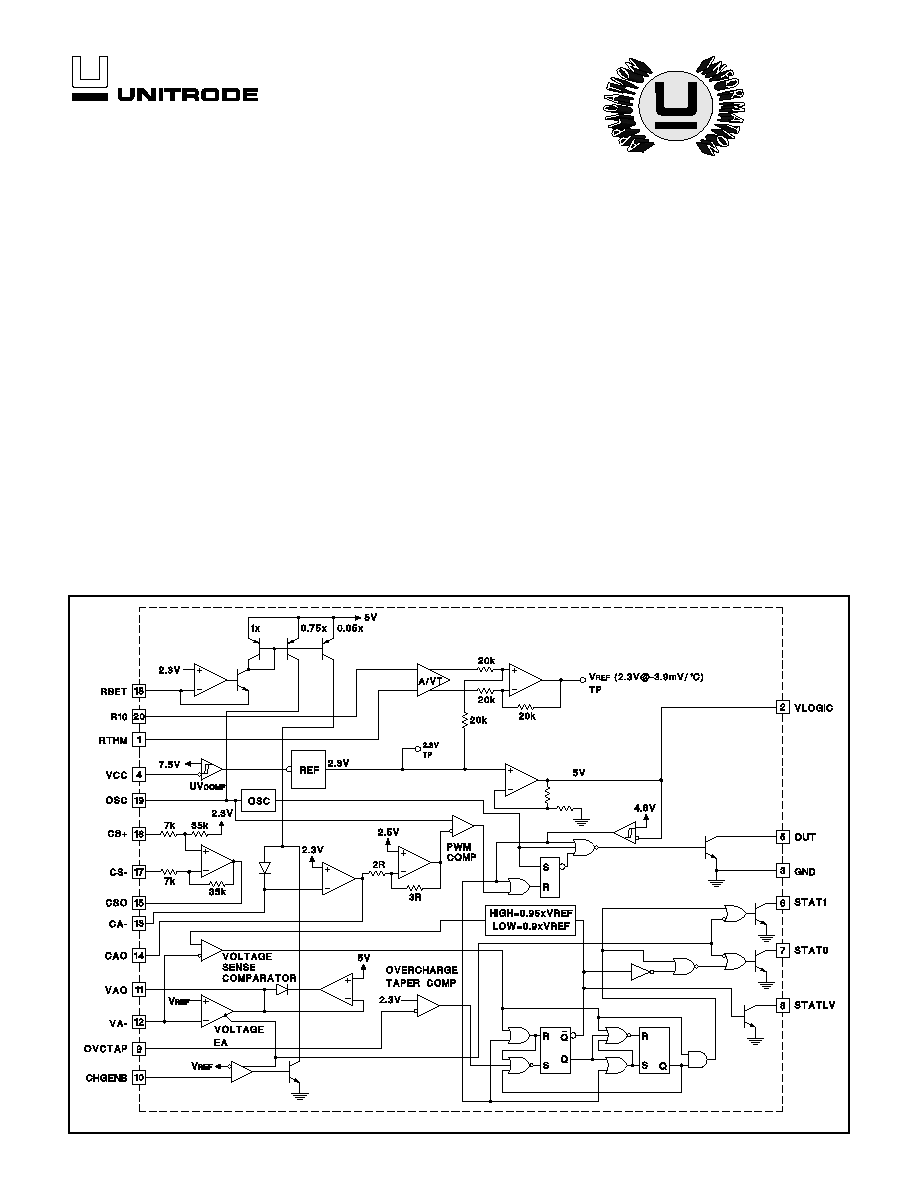
BLOCK DIAGRAM
UDG-95007-1
Pin numbers refer to J, N, DW packages.

2
UC2909
UC3909
DIL-20, (Top View)
J or N, DW Packages
ABSOLUTE MAXIMUM RATINGS
Supply Voltage (VCC), OUT, STAT0, STAT1 . . . . . . . . . . . 40V
Output Current Sink . . . . . . . . . . . . . . . . . . . . . . . . . . . . . . 0.1A
CS+, CS- . . . . . . . . . . . . . . . . . . . . . . . . . . -0.4 to VCC (Note 1)
Remaining Pin Voltages. . . . . . . . . . . . . . . . . . . . . . -0.3V to 9V
Storage Temperature . . . . . . . . . . . . . . . . . . . -65∞C to +150∞C
Junction Temperature . . . . . . . . . . . . . . . . . . . -55∞C to +150∞C
Lead Temperature (Soldering, 10 sec.) . . . . . . . . . . . . . +300∞C
All currents are positive into, negative out of the specified ter-
minal. Consult Packaging Section of Databook for thermal limi-
tations and considerations of packages.
Note 1: Voltages more negative than -0.4V can be tolerated if
current is limited to 50mA.
CONNECTION DIAGRAMS
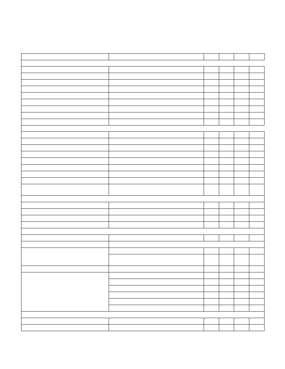
ELECTRICAL CHARACTERISTICS:
Unless otherwise stated these specifications apply for T
A
= ≠40∞C to +85∞C for
UC2909; ∞0C to +70∞C for UC3909; C
T
= 330pF, R
SET
= 11.5k, R10 = 10k, R
THM
= 10k, V
CC
= 15V, Output no load, R
STAT0
=
R
STAT1
= 10k, CHGENB = OVCTAP = VLOGIC, T
A
= T
J
.
PARAMETER
TEST CONDITIONS
MIN
TYP
MAX
UNITS
Current Sense AMP (CSA) Section
V
ID
= CS+ ≠ CS≠
DC Gain
CS≠ = 0, CS+ = -50mV; CS+ = ≠250mV
4.90
5
5.10
V/V
CS+ = 0, CS≠ = 50mV; CS≠- = 250mV
4.90
5
5.10
V/V
V
OFFSET
(V
CSO
≠ V
CAO
)
CS+ = CS≠ = 2.3V, CAO = CA≠
15
mV
CMRR
V
CM
= ≠0.25 to VCC ≠ 2, 8.8 < VCC < 14
50
dB
V
CM
= ≠0.25 to VCC, 14 < VCC < 35
50
dB
V
OL
V
ID
= ≠550mV, ≠0.25V < VCM < VCC≠2,
I
O
= 500
µ
A
0.3
0.6
V
V
OH
V
ID
= +700mV, ≠0.25V < VCM < VCC≠2,
I
O
= ≠250
µ
A
5.2
5.7
6.2
V
Output Source Current
V
ID
= +700mV, CSO = 4V
≠1
≠0.5
mA
Output Sink Current
V
ID
= ≠550mV, CSO = 1V
3
4.5
mA
3dB Bandwidth
V
ID
= 90mV, V
CM
= 0V
200
kHz
LCC-28, PLCC-28 (Top View)
L, Q Packages
3
UC2909
UC3909
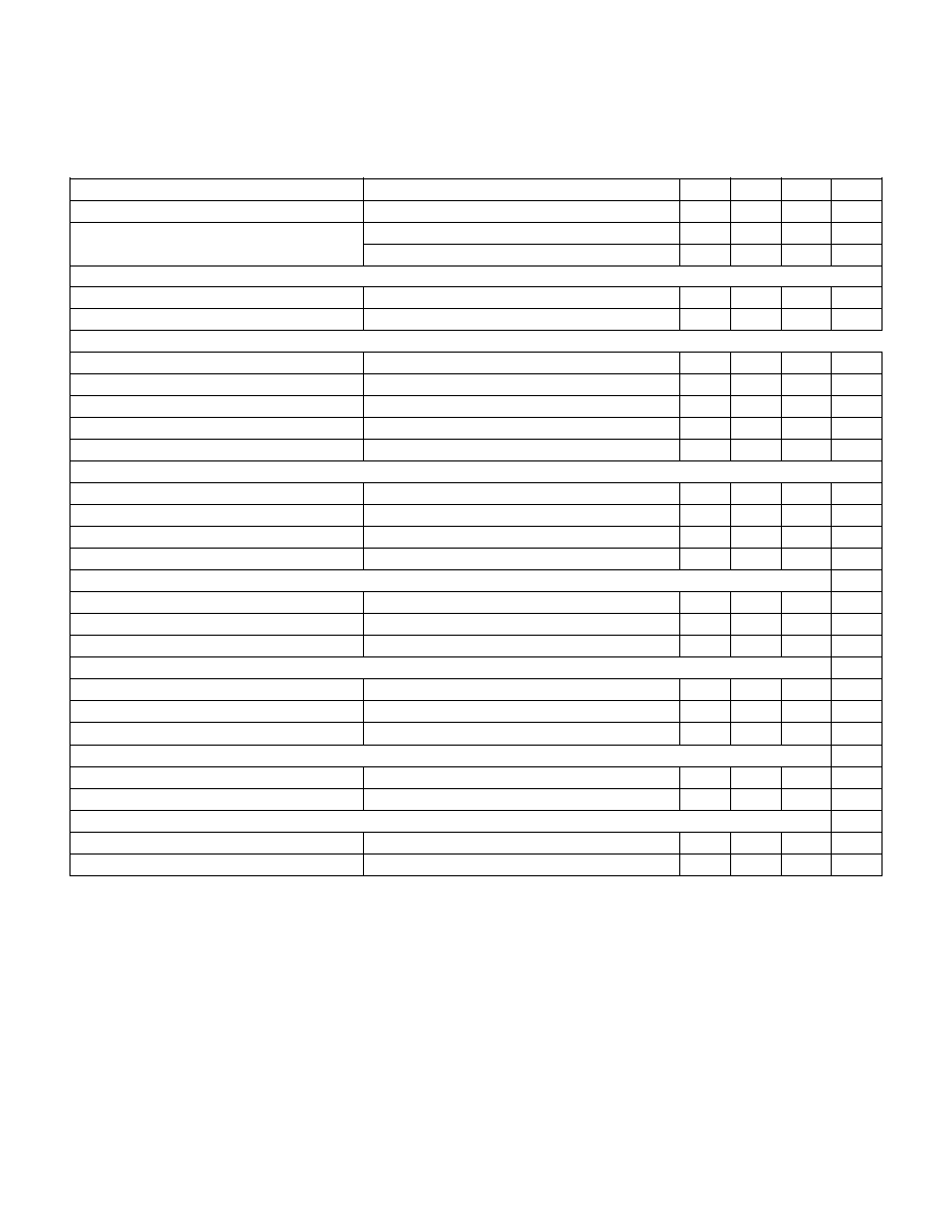
ELECTRICAL CHARACTERISTICS:
Unless otherwise stated these specifications apply for T
A
= ≠40∞C to +85∞C for
UC2909; ∞0C to +70∞C for UC3909; C
T
= 330pF, R
SET
= 11.5k, R10 = 10k, R
THM
= 10k, V
CC
= 15V, Output no load, R
STAT0
=
R
STAT1
= 10k, CHGENB = OVCTAP = VLOGIC, T
A
= T
J
.
PARAMETER
TEST CONDITIONS
MIN
TYP
MAX
UNITS
Current Error Amplifier (CEA) Section
I
B
8.8V < VCC < 35V, V
CHGENB
= V
LOGIC
0.1
0.8
µ
A
V
IO
(Note 2)
8.8V < VCC < 35V, CAO = CA≠
10
mV
A
VO
1V < VAO < 4V
60
90
dB
GBW
T
J
= 25∞C, F = 100kHz
1
1.5
MHz
V
OL
I
O
= 250
µ
A
0.4
0.6
V
V
OH
I
O
= ≠5mA
4.5
5
V
Output Source Current
CAO = 4V
≠25
≠12
mA
Output Sink Current
CAO = 1V
2
3
mA
I
CA
≠, I
TRCK_CONTROL
V
CHGENB
= GND
8.5
10
11.5
µ
A
Voltage Amplifier (CEA) Section
I
B
Total Bias Current; Regulating Level
0.1
1
µ
A
V
IO
(Note 2)
8.8V < VCC < 35V, VCM = 2.3V, VAO = VA≠
1.2
mV
A
VO
1V < CAO < 4V
60
90
dB
GBW
T
J
= 25∞C, F = 100kHz
0.25
0.5
MHz
V
OL
I
O
= 500
µ
A
0.4
0.6
V
V
OH
I
O
= ≠500
µ
A
4.75
5
5.25
V
Output Source Current
CAO = 4V
≠2
≠1
mA
Output Sink Current
CAO = 1V
2
2.5
mA
VAO Leakage: High Impedance State
V
CHGENB
= GND, STAT0 = 0 & STAT1 = 0,
VAO = 2.3V
≠1
1
µ
A
Pulse Width Modulator Section
Maximum Duty Cycle
CAO = 0.6V
90
95
100
%
Modulator Gain
CAO = 2.5V, 3.2V
63
71
80
%/V
OSC Peak
3
V
OSC Valley
1
V
Oscillator Section
Frequency
8.8V < VCC < 35V
198
220
242
kHz
Thermistor Derived Reference Section
V
ID
= V
RTHM
≠ V
R10
Initial Accuracy, VAO (RTHM = 10k)
V
ID
= 0, R10 = RTHM =10k (Note 3)
2.2655
2.3
2.3345
V
V
ID
= 0, R10 = RTHM =10k, ≠40∞C
T
A
< 0∞C
(Note 3)
2.254
2.3
2.346
V
Line Regulation
V
CC
= 8.8V to 35V
3
10
mV
VAO
RTHM = 138k, R10 = 10k
2.458
2.495
2.532
V
RTHM = 138k, R10 = 10k, -40∞C
T
A
< 0∞C
2.445
2.495
2.545
V
RTHM = 33.63k, R10 = 10k
2.362
2.398
2.434
V
RTHM = 33.63k, R10 = 10k, -40∞C
T
A
< 0∞C
2.350
2.398
2.446
V
RTHM = 1.014k, R10 = 10k
2.035
2.066
2.097
V
RTHM = 1.014k, R10 = 10k, -40∞C
T
A
< 0∞C
2.025
2.066
2.107
V
Charge Enable Comparator Section (CEC)
Threshold Voltage
As a function of VA≠
0.99
1
1.01
V/V
Input Bias Current
CHGENB = 2.3V
≠0.5
≠0.1
µ
A
4
UC2909
UC3909
ELECTRICAL CHARACTERISTICS:
Unless otherwise stated these specifications apply for T
A
= ≠40∞C to +85∞C for
UC2909; ∞0C to +70∞C for UC3909; C
T
= 330pF, R
SET
= 11.5k, R10 = 10k, R
THM
= 10k, V
CC
= 15V, Output no load, R
STAT0
=
R
STAT1
= 10k, CHGENB = OVCTAP = VLOGIC, T
A
= T
J
.
PARAMETER
TEST CONDITIONS
MIN
TYP
MAX
UNITS
Voltage Sense Comparator Section (VSC)
Threshold Voltage
STAT0 = 0, STAT1 = 0, Function of V
REF
0.945
0.95
0.955
V/V
STAT0 = 1, STAT1 = 0, Function of V
REF
0.895
0.9
0.905
V/V
Over Charge Taper Current Comparator Section (OCTIC)
Threshold Voltage
Function of 2.3V REF, CA- = CAO
0.99
1
1.01
V/V
Input Bias Current
OVCTAP = 2.3V
≠0.5
≠0.1
µ
A
Logic 5V Reference Section (VLOGIC)
VLOGIC
VCC = 15V
4.875
5.0
5.125
V
Line Regulation
8.8V < V
CC
< 35V
3
15
mV
Load Regulation
0 < I
O
< 10mA
3
15
mV
Reference Comparator Turn-on Threshold
4.3
4.8
V
Short Circuit Current
V
REF
= 0V
30
50
80
mA
Output Stage Section
I
SINK
Continuous
50
mA
I
PEAK
100
mA
V
OL
I
O
=50mA
1
1.3
V
Leakage Current
V
OUT
=35V
25
µ
A
STAT0 & STAT1 Open Collector Outputs Section
Maximum Sink Current
V
OUT
= 8.8V
6
10
mA
Saturation Voltage
I
OUT
= 5mA
0.1
0.45
V
Leakage Current
V
OUT
= 35V
25
µ
A
STATLV Open Collector Outputs Section
Maximum Sink Current
V
OUT
= 5V
2.5
5
mA
Saturation Voltage
I
OUT
= 2mA
0.1
0.45
V
Leakage current
V
OUT
= 5V
3
µ
A
UVLO Section
Turn-on Threshold
6.8
7.8
8.8
V
Hysteresis
100
300
500
mV
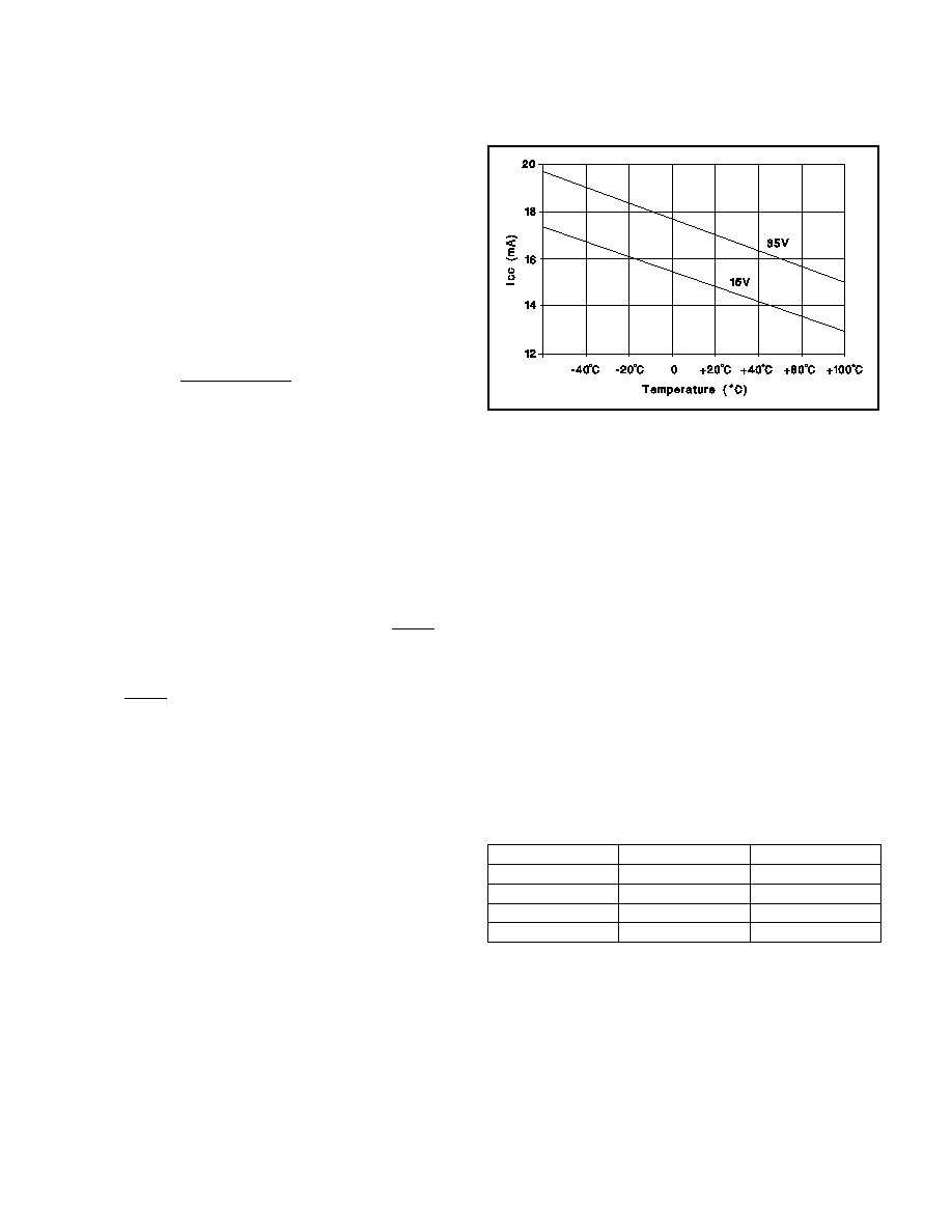
I
CC
Section
I
CC
(run)
(See Fig. 1)
13
19
mA
I
CC
(off)
VCC = 6.5V
2
mA
Note 2: VIO is measured prior to packaging with internal probe pad.
Note 3: Thermistor initial accuracy is measured and trimmed with respect to VAO; VAO = VA≠.
CA≠: The inverting input to the current error amplifier.
CAO: The output of the current error amplifier which is
internally clamped to approximately 4V. It is internally
connected to the inverting input of the PWM comparator.
CS≠, CS+: The inverting and non-inverting inputs to the
current sense amplifier. This amplifier has a fixed gain of
five and a common-mode voltage range of from ≠250mV
to +VCC.
CSO: The output of the current sense amplifier which is
internally clamped to approximately 5.7V.
CHGENB: The input to a comparator that detects when
battery voltage is low and places the charger in a trickle
charge state. The charge enable comparator makes the
output of the voltage error amplifier a high impedance
while forcing a fixed 10
µ
A into CA≠ to set the trickle
charge current.
PIN DESCRIPTIONS
5
UC2909
UC3909
GND: The reference point for the internal reference, all
thresholds, and the return for the remainder of the de-
vice. The output sink transistor is wired directly to this
pin.
OVCTAP: The overcharge current taper pin detects
when the output current has tapered to the float thresh-
old in the overcharge state.
OSC: The oscillator ramp pin which has a capacitor (C
T
)
to ground. The ramp oscillates between approximately
1.0V to 3.0V and the frequency is approximated by:
frequency
C
R
T
SET
=
∑
∑
1
1 2
.
OUT: The output of the PWM driver which consists of an
open collector output transistor with 100mA sink capabil-
ity.
R10: Input used to establish a differential voltage corre-
sponding to the temperature of the thermistor. Connect
a 10k resistor to ground from this point.
RSET:
A resistor to ground programs the oscillator
charge current and the trickle control current for the oscil-
lator ramp.
The oscillator charge current is approximately
1 75
.
R
SET
.
The trickle control current (I
TRCK_CONTROL
) is approxi-
mately
0115
.
R
SET
.
RTHM: A 10k thermistor is connected to ground and is
thermally connected to the battery. The resistance will
vary exponentially over temperature and its change is
used to vary the internal 2.3V reference by ≠3.9mV/∞C.
The recommended thermistor for this function is part
number L1005-5744-103-D1, Keystone Carbon Com-
pany, St. Marys, PA.
STAT0:
This open collector pin is the first decode bit
used to decode the charge states.
STAT1: This open collector pin is the second decode bit
used to decode the charge states.
STATLV: This bit is high when the charger is in the float
state.
VA≠: The inverting input to the voltage error amplifier.
VAO: The output of the voltage error amplifier. The up-
per output clamp voltage of this amplifier is 5V.
VCC: The input voltage to the chip. The chip is opera-
tional between 7.5V and 40V and should be bypassed
with a 1
µ
F capacitor. A typical I
CC
vs. temperature is
shown in Figure 1.
VLOGIC: The precision reference voltage. It should be
bypassed with a 0.1
µ
F capacitor.
Charge State Decode Chart
STAT0 and STAT1 are open collector outputs. The out-
put is approximately 0.2V for a logic 0.
STAT1
STAT0
Trickle Charge
0
0
Bulk Charge
0
1
Over Charge
1
0
Float Charge
1
1
PIN DESCRIPTIONS (cont.)
Figure 1. I
CC
vs. temperature.