 | –≠–ª–µ–∫—Ç—Ä–æ–Ω–Ω—ã–π –∫–æ–º–ø–æ–Ω–µ–Ω—Ç: UDT-455LN | –°–∫–∞—á–∞—Ç—å:  PDF PDF  ZIP ZIP |
PhotopsTM
Photodiode-Amplifier Hybrids
"
FEATURES
∑ Detector/Amplifier
Combined
∑ Adjustable Gain/Bandwidth
∑ Low Noise
∑ Wide Bandwidth
∑ DIP Package
∑ Large Active Area
"
APPLICATIONS
∑ General Purpose Light
Detection
∑ Laser Power Monitoring
∑ Medical Analysis
∑ Laser Communications
∑ Bar Code Readers
∑ Industrial Control Sensors
∑ Pollution Monitoring
∑ Guidance Systems
∑ Colorimeter
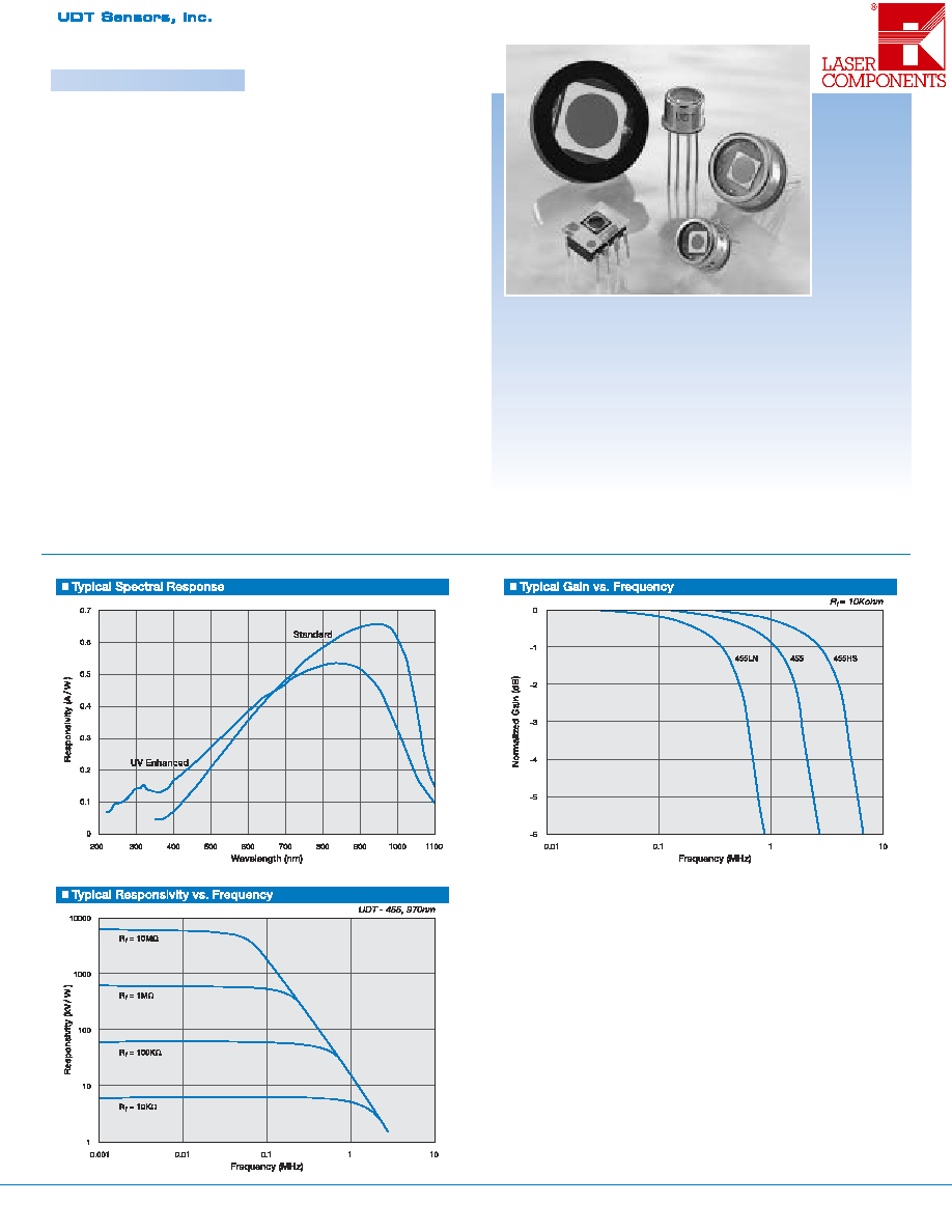
The PhotopTM Series, combines a photodiode with an operational
amplifier in the same package. PhotopsTM general-purpose detectors
have a spectral range from either 350 nm to 1100 nm or 200 nm to
1100nm. They have an integrated package ensuring low noise output
under a variety of operating conditions. These op-amps are specifically
selected by UDT Sensors engineers for compatibility to our photodiodes.
Among many of these specific parameters are low noise, low drift and
capability of supporting a variety of gains and bandwidths determined by
the external feedback components. Operation from DC level to several
MHz is possible in an either unbiased configuration for low speed, low
drift applications or biased for faster response time. LN-Series PhotopsTM
are to be used with OV-bias.
Any modification of the above devices is possible. The modifications
can be simply adding a bandpass optical filter, integration of additional
chip (hybrid) components inside the same package, utilizing a different
op-amp, photodetector replacement, modified package design and / or
mount on PCB or ceramic. For your specific requirements, contact one
of our Applications Engineers.
Great Britain: LASER COMPONENTS (UK) Ltd., Phone: +44 1245 491 499, Fax: +44 1245 491 801, info@lasercomponents.co.uk

Active
Area
Responsivity
(A/W)
Capacitance
(pF)
Dark
Current
(nA)
Shunt
Resistance
(M
)
NEP
(W/Hz)
Reverse Voltage
Temp.*
Range
(∞C)
254 nm
970 nm
0 V
-10 V
-10 V
-10
mV
0 V
254 nm
-10V
970 nm
V
Model Number
Area (mm
2
)
Dimension
(mm)
min.
typ.
min.
typ.
typ.
typ.
typ.
max.
typ.
typ.
typ.
max.
Operating
Storage
Package
Style ∂
350-1100 nm Spectral Range
UDT-451
29 / DIP
UDT-455
UDT-455LN**
UDT-455HS
5.1
2.54
85
15
0.25
3
1.4 e- 14
30 / TO-5
UDT-020D
16
4.57
330
60
0.5
10
1.9 e- 14
31 / TO-8
UDT-555D
100
11.3
---
0.60
0.65
1500
300
2
25
---
3.9 e -14
30**
32 / Special
200-1100 nm Spectral Range
UDT-455UV
UDT-
455UV/LN**
5.1
2.54
300
100
9.2 e -14
30 / TO-5
UDT-020UV
16
4.57
1000
50
1.3 e -13
31 / TO-8
UDT-055UV
50
7.98
2500
20
2.1 e -13
32 / Special
UDT-555UV
UDT-
555UV/LN**
100
11.3
0.10
0.14
---
4500
---
10
2.9 e -13
---
5**
0 ~ +70
-30 ~ +100
32 / Special
Operational Amplifier Specifications
Typical Electro-Optical Specifications at T
A
=23 ∫C
Input
Noise
Voltage
Input
Noise
Current
Quiescent
Supply
Current
(mA)
Input
Offset
Voltage
Temp.
Coefficient Input Offset
Voltage
Input Bias
Current
Gain
Bandwidth
Product
Slew Rate
Open Loop
Gain, DC
100 Hz
1 kHz
1 kHz
Supply
Voltage
(V)
± 15 V
mV
µV / ∫C
pA
MHz
V / µs
V / mV
nV/Hz
fA/Hz
Model Number
min.
typ.
max.
typ.
max.
typ.
max.
typ.
max.
typ.
max.
min.
typ.
min.
typ.
min.
typ.
typ.
typ.
typ.
UDT-451
---
±15
±18
1.4
2.5
3.0
6.0
10
---
30
200
---
4.0
---
13
50
150
---
18
10
UDT-455
UDT-455UV
UDT-020D
UDT-020UV
--- ±15
±18
2.8
5.0
0.5
3
4
30
±80
±400
3.0
5.4
5
9
50
200
20
15
10
UDT-455HS
---
±15
±18
4.8
8.0
0.5
3
4
30
±80
±500
11
26
25
40
50
200
20
15
10
UDT-455LN**
UDT-
455UV/LN**
±5
±15
±18
0.9
1.8
0.26
1
---
20
0.15
0.3
0.5
1
0.5
3
50
2500
78
27
0.22
UDT-055UV
UDT-555D
UDT-555UV
---
±15
±22
2.7
4.0
0.4
1
3
10
±40
±200
3.5
5.7
7.5
11
75
220
20
15
10
PhotopsTM (Photodiode Specifications)
Typical Electro-Optical Specifications at T
A
=23∫C
∂ For mechanical drawings please refer to pages 55 thru 66.
** LN ≠ Series Devices are to be used with a 0V Bias.
* Non-Condensing temperature and Storage Range, Non-Condensing Environment.
Great Britain: LASER COMPONENTS (UK) Ltd., Phone: +44 1245 491 499, Fax: +44 1245 491 801, info@lasercomponents.co.uk

Photop Series
Schematic Diagrams
The output voltage is proportional to the light intensity of the light and is
given by:
(1)
Frequency Response (Photodiode/Amplifier Combination)
The frequency response of the photodiode / amplifier combination is
determined by the characteristics of the photodetector, pre-amplifier as
well as the feedback resistor (R
F
) and feedback capacitor (C
F
). For a
known gain, (R
F
), the 3dB frequency response of the detector/pre-amp
combination is given by:
(2)
However, the desired frequency response is limited by the Gain
Bandwidth Product (GBP) of the op-amp. In order to have a stable
output, the values of the R
F
and C
F
must be chosen such that the 3dB
frequency response of the detector / pre-amp combination, be less than
the maximum frequency of the op-amp, i.e. f
3dB
f
max
.
(3)
where C
A
is the amplifier input capacitance.
In conclusion, an example for frequency response calculations, is given
below. For a gain of 10
8
, an operating frequency of 100 Hz, and an op-
amp with GBP of 5 MHz:
(4)
Thus, for C
F
= 15.9 pF, C
J
= 15 pF and C
A
= 7 pF, f
max
is about 14.5 kHz.
Hence, the circuit is stable since f
3dB
f
max
.
For more detailed application specific discussions and further reading,
refer to the APPLICATION NOTES INDEX in the catalog.
Note: The shaded boxes represent the PhotopTM components and their
connections. The components outside the boxes are typical
recommended connections and components.
Great Britain: LASER COMPONENTS (UK) Ltd., Phone: +44 1245 491 499, Fax: +44 1245 491 801, info@lasercomponents.co.uk

Photodiode Care and Handling Instructions
AVOID DIRECT LIGHT
Since the spectral response of silicon photodiode includes the visible light region, care must be taken to avoid photodiode exposure to high ambient
light levels, particularly from tungsten sources or sunlight. During shipment from UDT Sensors, your photodiodes are packaged in opaque, padded
containers to avoid ambient light exposure and damage due to shock from dropping or jarring.
AVOID SHARP PHYSICAL SHOCK
Photodiodes can be rendered inoperable if dropped or sharply jarred. The wire bonds are delicate and can become separated from the photodiode's
bonding pads when the detector is dropped or otherwise receives a sharp physical blow.
CLEAN WINDOWS WITH OPTICAL GRADE CLOTH / TISSUE
Most windows on UDT Sensors photodiodes are either silicon or quartz. They should be cleaned with isopropyl alcohol and a soft (optical grade) pad.
OBSERVE STORAGE TEMPERATURES AND HUMIDITY LEVELS
Photodiode exposure to extreme high or low storage temperatures can affect the subsequent performance of a silicon photodiode. Storage temperature
guidelines are presented in the photodiode performance specifications of this catalog. Please maintain a non-condensing environment for optimum
performance and lifetime.
OBSERVE ELECTROSTATIC DISCHARGE (ESD) PRECAUTIONS
UDT Sensors photodiodes, especially with IC devices (e.g. Photops) are considered ESD sensitive. The photodiodes are shipped in ESD protective
packaging. When unpacking and using these products, anti-ESD precautions should be observed.
DO NOT EXPOSE PHOTODIODES TO HARSH CHEMICALS
Photodiode packages and/or operation may be impaired if exposed to CHLOROTHENE, THINNER, ACETONE, or TRICHLOROETHYLENE.
INSTALL WITH CARE
Most photodiodes in this catalog are provided with wire or pin leads for installation in circuit boards or sockets. Observe the soldering temperatures and
conditions specified below:
Photodiodes in plastic packages should be given special care. Clear plastic packages are more sensitive to environmental stress than those of black
plastic. Storing devices in high humidity can present problems when soldering. Since the rapid heating during soldering stresses the wire bonds and can
cause wire to bonding pad separation, it is recommended that devices in plastic packages to be baked for 24 hours at 85∞C.
The leads on the photodiode SHOULD NOT BE FORMED. If your application requires lead spacing modification, please contact UDT Sensors
Applications group at (310)978-0516 before forming a product's leads. Product warranties could be voided.
Soldering Iron:
Soldering 30 W or less
Temperature at tip of iron 300∞C or lower.
Dip Soldering:
Bath Temperature:
260±5∞C.
Immersion Time:
within 5 Sec.
Soldering Time:
within 3 Sec.
Vapor Phase Soldering:
DO NOT USE
Reflow Soldering:
DO NOT USE
Great Britain: LASER COMPONENTS (UK) Ltd., Phone: +44 1245 491 499, Fax: +44 1245 491 801, info@lasercomponents.co.uk

1. Parameter Definitions:
A = Distance from top of chip to top of glass.
a = Photodiode Anode.
B = Distance from top of glass to bottom of case.
c = Photodiode Cathode
(Note: cathode is common to case in metal package products unless otherwise noted).
W = Window Diameter.
F.O.V. = Filed of View (see definition below).
2. Dimensions are in inches (1 inch = 25.4 mm).
3. Pin diameters are 0.018 ± 0.002" unless otherwise specified.
4. Tolerances
(unless otherwise noted)
General: 0.XX ±0.01"
0.XXX ±0.005"
Chip Centering: ±0.010"
Dimension `A': ±0.015"
5. Windows
All `UV' Enhanced products are provided with QUARTZ glass windows,
0.027 ± 0.002" thick.
All `XUV' products are provided with removable windows.
All `DLS' PSD products are provided with A/R coated glass windows.
All `FIL' photoconductive and photovoltaic products are epoxy filled instead of
glass windows.
Great Britain: LASER COMPONENTS (UK) Ltd., Phone: +44 1245 491 499, Fax: +44 1245 491 801, info@lasercomponents.co.uk