1
Standard Products
UT63M1XX MIL-STD-1553A/B Bus Transceiver
Data Sheet
Sept. 1999
FEATURES
q Full conformance to MIL-STD-1553A and 1553B
q Completely monolithic bipolar technology
q Low power consumption
q Fit and functionally compatible to industry standard 631XX
series
q Idle low encoding version
q Flexible power supply voltages: V
CC
=+5V, V
EE
=-12V or -
15V, and V
CCA
=+5V to +12V or +5V to +15V
q Full military operating temperature range, -55
∞
C to +125
∞
C,
screened to QML Q or QML V requirements
q Standard Military Drawing available
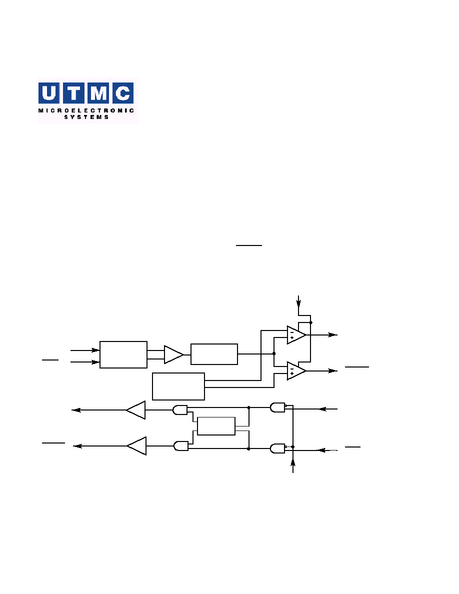
INTRODUCTION
The monolithic UT63M1XX Transceivers are complete
transmitter and receiver pairs conforming fully to MIL-STD-
1553A and 1553B. Encoder and decoder interfaces are idle low.
UTMC's advanced bipolar technology allows the positive
analog power to range from +5V to +12V or +5V to +15V,
providing more flexibility in system power supply design.
The receiver section of the UT63M1XX series accepts biphase-
modulated Manchester II bipolar data from a MIL-STD-1553
data bus and produces TTL-level signal data at its RXOUT and
RXOUT outputs. An external RXEN input enables or disables
the receiver outputs.
TXIN
RXOUT
RXEN
FROM ENCODER
TO DECODER
DRIVERS
COMPARE
FILTER
LIMITER
and
FILTER
TXIHB
Figure 1. Functional Block Diagram
RXIN
TXOUT
RXIN
TXOUT
RXOUT
TXIN
THRESHOLD
REFERENCE

2
Legend for TYPE field:
TI = TTL input
TO = TTL output
DO = Differential output
DI = Differential input
() = Channel designator
TRANSMITTER
NAME
PACKAGE PIN
TYPE
DESCRIPTION
SINGLE
DUAL
TXOUT
(A)
1
1
DO
Transmitter outputs: TXOUT and TXOUT are differential data signals.
TXOUT
(B)
N/A
10
DO
TXOUT
(A)
2
2
DO
TXOUT is the complement of TXOUT.
TXOUT
(B)
N/A
11
DO
TXIHB
(A)
21
34
TI
Transmitter inhibit: this is an active high input signal.
TXINB
(B)
N/A
25
TI
TXIN
(A)
22
35
TI
Transmitter inputs: TXIN and TXIN are complementary TTL-level
Manchester II encoder inputs.
TXIN
(B)
N/A
26
TI
TXIN
(A)
23
36
TI
TXIN is the complement of TXIN input.
TXIN
(B)
N/A
27
TI
The transmitter section accepts biphase TTL-level signal data
at its TXIN and TXIN and produces MIL-STD-1553 data
signals. The transmitter's output voltage is typically 42V
PP
, L-
L. Activating the TXIHB input or setting both data inputs to
the same logic level disables the transmitter.
The UT63M1XX series offers a monolithic transmitter and
receiver packaged in either single channel (24-pin) or dual-
channel (36-pin) configurations designed for use in any MIL-
STD-1553 application.

3
RECEIVER
NAME
PACKAGE PIN
TYPE
DESCRIPTION
SINGLE
DUAL
RXOUT
(A)
7
5
TO
Receiver outputs: RXOUT and RXOUT are complementary
Manchester II decoder outputs.
RXOUT
(B)
N/A
14
TO
RXOUT
(A)
10
8
TO
RXOUT is the complement of RXOUT output
RXOUT
(B)
N/A
17
TO
RXEN
(A)
8
6
TI
Receiver enable/disable: This is an active high input signal.
RXEN
(B)
N/A
15
TI
RXIN
(A)
15
29
DI
Receiver inputs: RXIN and RXIN are biphase-modulated Manchester
II bipolar inputs from MIL-STD-1553 data bus.
RXIN
(B)
N/A
20
DI
RXIN
(A)
16
30
DI
RXIN is the complement of RXIN input.
RXIN
(B)
N/A
21
DI
POWER AND GROUND
NAME
PACKAGE PIN
TYPE
DESCRIPTION
SINGLE
DUAL
V
CC
(A)
20
33
PWR
+5V
DC
power (
±
10%)
V
CC
(B)
N/A
24
PWR
V
CCA
(A)
13
28
PWR
+5 to +12V
DC
power or
+5 to +15V
DC
power (
±
5%)
V
CCA
(B)
N/A
19
PWR
V
EE
(A)
19
32
PWR
-12 or -15V
DC
power (
±
5%)
Recommended de-coupling capacitors 4.7
µ
F and.1
µ
F
V
EE
(B)
N/A
23
PWR
GND
(A)
3, 9, 18
3, 7, 31
GND
Ground reference
GND
(B)
N/A
12, 16, 22
GND
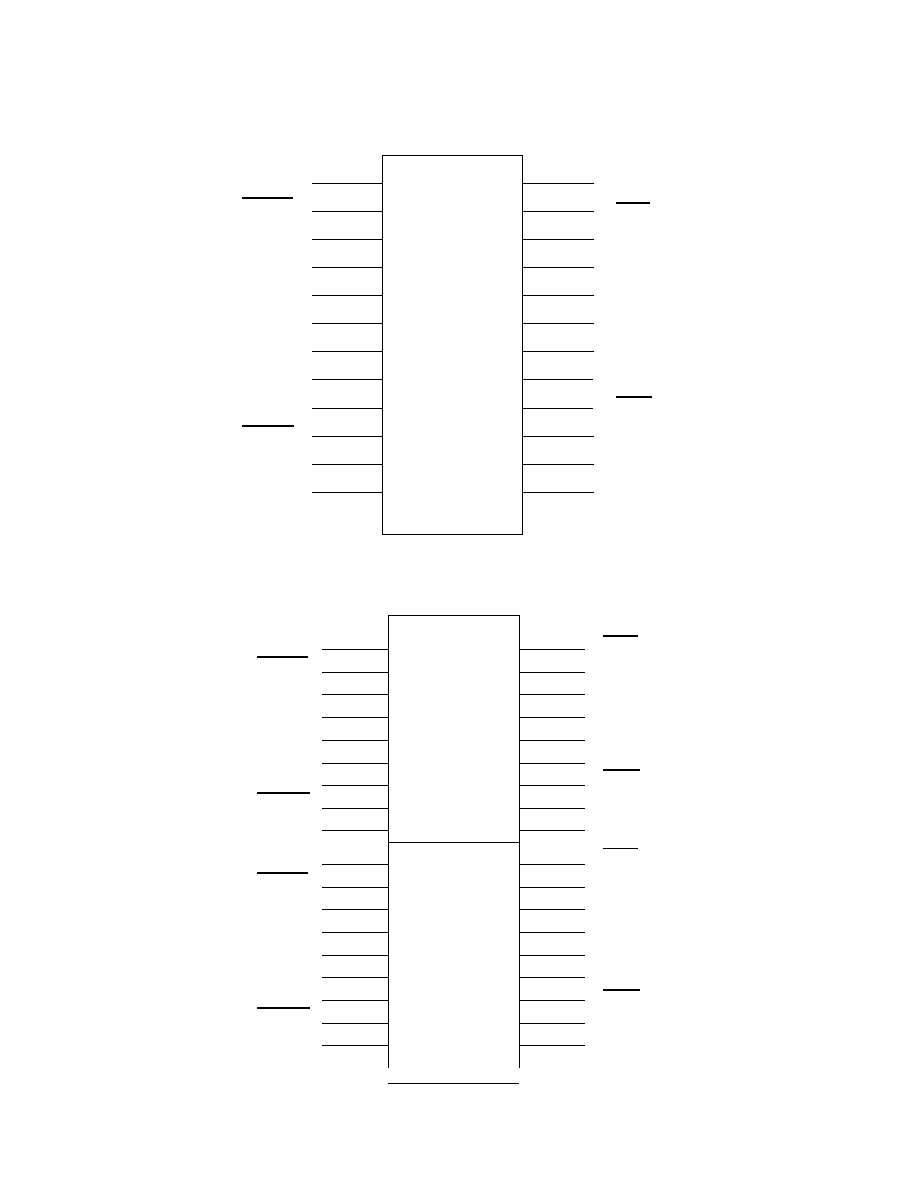
4
RXEN
RXOUT
TXOUT
RXIN
TXIN
24
23
22
21
20
19
18
17
16
15
14
13
12
11
10
9
8
7
6
5
4
3
2
1
NC
NC
GND
NC
NC
NC
GND
NC
NC
GND
NC
CHANNEL
Figure 2a. Functional Pin Diagram--Single Channel
TXIHB
TXOUT
RXOUT
TXIN
RXIN
V
CCA
V
CC
V
EE
A
RXIN
TXIN
RXIN
TXIN
TXOUT
RXOUT
RXOUT
RXEN
RXEN
TXOUT
36
26
10
11
13
14
15
17
18
16
27
28
CHANNEL
35
34
33
32
31
30
29
26
25
24
23
22
B
21
20
19
CHANNEL
1
2
3
4
5
A
6
7
8
9
12
GND
GND
GND
NC
GND
NC
GND
NC
GND
NC
TXIHB
TXIHB
Figure 2b. Functional Pin Diagram--Dual Channel
TXOUT
RXOUT
TXIN
RXIN
TXOUT
RXIN
TXIN
RXOUT
V
CCA
V
CCA
V
CC
V
EE
V
CC
V
EE

5
TRANSMITTER
The transmitter section accepts Manchester II biphase TTL data
and converts this data into differential phase-modulated current
drive. Transmitter current drivers are coupled to a MIL-STD-
1553 data bus via a transformer driven from the TXOUT and
TXOUT terminals. Transmitter output terminals' non-
transmitting state is enabled by asserting TXIHB (logic 1), or
by placing both TXIN and TXIN at the same logic level. Table
1, Transmit Operating Mode, lists the functions for the output
data in reference to the state of TXIHB. Figure 3 shows typical
transmitter waveforms.
RECEIVER
The receiver section accepts biphase differential data from a
MIL-STD-1553 data bus at its RXIN and RXIN inputs. The
receiver converts input data to biphase Manchester II TTL
format and is available for decoding at the RXOUT and RXOUT
terminals. The outputs RXOUT and RXOUT represent positive
and negative excursions (respectively) of the inputs RXIN and
RXIN. Figure 4 shows typical receiver output waveforms.
Models UT63M105, UT63M107, UT63M125, and UT63M127
idle in the "0" state when disabled or receiving no signal.
POWER SUPPLY VOLTAGES
The UT63M1XX series meets device requirements over a wide
range of power supply voltages. Table 2 shows the overall
capabilities of all available devices. Each channel of the dual
transceiver is electrically and physically separate from the other
and fully independent, including all power and signal lines. Thus
there will be no interaction between the channels.
Notes:
1. x = Don't care.
2. Transmitter output terminals are in the non-transmitting mode during Off
time.
3. Transmitter output terminals are in the non-transmitting mode during Off
time, independent of TXIHB status.
Table 1. Transmit Operating Mode
TXIN
TXIN
TXIHB
TXOUT
x
1
x
1
Off
2
0
0
x
Off
3
0
1
0
On
1
0
0
On
1
1
x
Off
3
TXIN
Figure 3. Typical Transmitter Waveforms
TXIN
t
TXDD
90%
10%
TXOUT, TXOUT
TXIN
LINE-TO-LINE
DIFFERENTIAL
OUTPUT
TXIN
TXIHB
BOTH HIGH
OR
BOTH LOW

6
DATA BUS INTERFACE
The designer can connect the UT63M1XX to the data bus via a
short-stub (direct-coupling) connection or a long-stub
(transformer-coupling) connection. Use a short-stub connection
when the distance from the isolation transformer to the data bus
does not exceed a one-foot maximum. Use a long-stub
connection when the distance from the isolation transformer
exceeds the one-foot maximum and is less than twenty-five feet.
Figure 5 shows various examples of bus coupling
configurations. The UT63M1XX series transceivers are
designed to function with MIL-STD-1553A and 1553B
compatible transformers.
RECOMMENDED THERMAL PROTECTION
All packages, single and dual, should mount to or contact a heat
removal rail located in the printed circuit board. To insure proper
heat transfer between the package and the heat removal rail, use
a thermally conductive material between the package and the
heat removal rail. Use a material such as Mereco XLN-589 or
equivalent to insure heat transfer between the package and heat
removal rail.
Figure 4. Typical Receiver Waveforms
QUIESCENT IDLE LOW
RXOUT
RXOUT
LINE-TO-LINE
DIFFERENTIAL
INPUT
RXOUT
RXOUT
t
RXDD
Table 2. Transceiver Model Capabilities
MODEL
V
CC
V
EE
V
CCA
IDLE
UT63M105
+5V
-15V
+5 to +15V
Low
UT63M107
+5V
-12V
+5 to +12V
Low
UT63M125
+5V
-15V
+5 to +15V
Low
UT63M127
+5V
-12V
+5 to +12V
Low

7
20 FT MAX
Figure 5. Bus Coupling Configuration
OPERATION
55 OHMS
55 OHMS
1 FT MAX
SHORT-STUB
DIRECT COUPLING
LONG-STUB
TRANSFORMER COUPLING
1:1.4
OPERATION
55 OHMS
55 OHMS
1 FT MAX
20 FT MAX
SHORT-STUB
DIRECT COUPLING
LONG-STUB
TRANSFORMER COUPLING
1.4:1
2:1
1:1.4
1.2:1
1.66:1
Note:
Z
O
defined per MIL-STD-1553B in section 4.5.1.5.2.1.
±
15V
DC
±
12V
DC
Z
O
.75Z
O
.75Z
O
Z
O
.75Z
O
.75Z
O
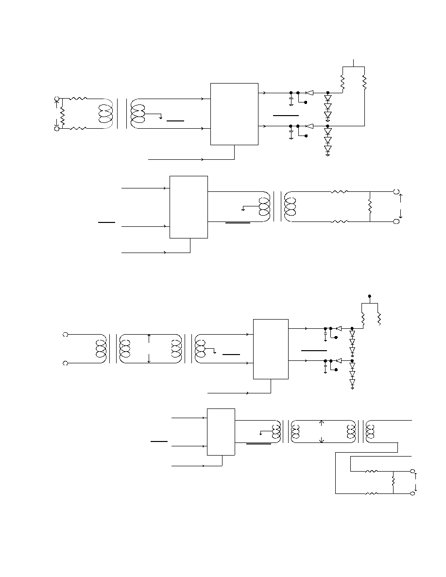
8
V
IN
R
L
=
55 OHMS
55 OHMS
35 OHMS
A
2K OHMS
2K OHMS
RECEIVER
TRANSMITTER
TP
TP
*
1:1.4
1.4:1
RXIN
RXEN
TXIN
TXOUT
RXOUT
TXIHB
55 OHMS
55 OHMS
35 OHMS
Notes:
1. TP = Test point.
2. R
L
removed for terminal input impedance test.
3. TX and RX tied together.
RXIN
TXIN
TXOUT
15pF
15pF
V
CC
RXOUT
Figure 6. Direct-Coupled Transceiver with Load
V
IN
Figure 7. Transformer-Coupled Transceiver with Load
1:1.4
2K OHMS
2K OHMS
RECEIVER
TP
TP
TRANSMITTER
55 OHMS
55 OHMS
35 OHMS
A
TXIHB
TXIN
RXEN
TXOUT N:L
L:N
1.4:1
RXIN
RXOUT
*
Notes:
1. TP = Test point.
2. N:L Ratio is dependent on power supply voltage.
3. R
L
removed for terminal input impedance test.
4. TX and RX tied together.
RXIN
TXIN
TXOUT
RXOUT
15pF
15pF

9
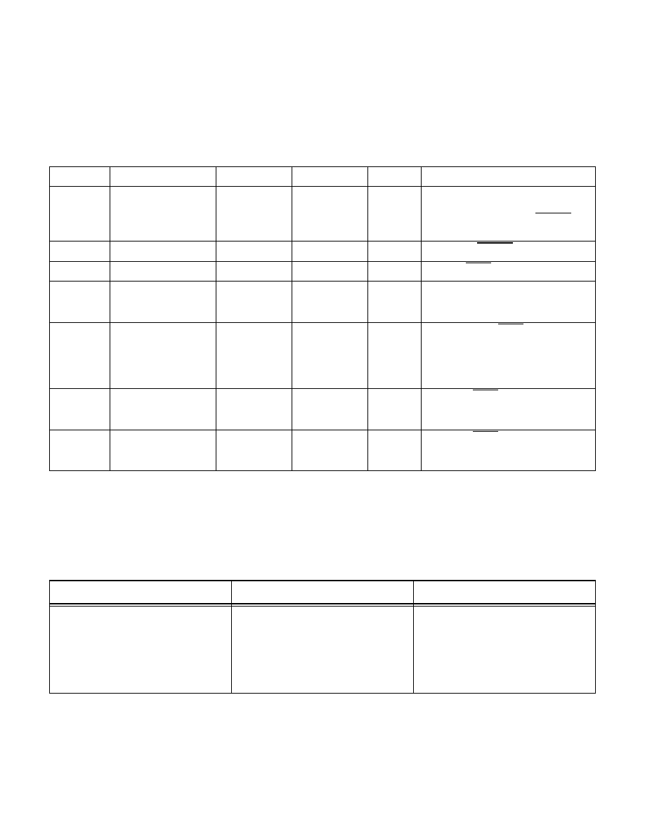
ABSOLUTE MAXIMUM RATINGS
1
(Referenced to V
SS
)
RECOMMENDED OPERATING CONDITIONS
SYMBOL
PARAMETER
LIMITS
UNIT
V
CC
Supply Voltage
7.0
V
V
EE
Supply Voltage
-22
V
V
CCA
Supply Voltage
+22
V
V
IN
Input Voltage Range (Receiver)
42
V
PP
, L-L
V
IN
Logic Input Voltage
-0.3 to +5.5
V
I
O
Output Current (Transmitter)
190
mA
P
D
Power Dissipation (per Channel)
4
W
Q
JC
Thermal Impedance, Junction-to-Case
6
2
∞
C/W
T
J
Operating Temperature, Junction
-55 to +150
∞
C
T
C
Operating Temperature, Case
-55 to +125
∞
C
T
STG
Storage Temperature
-65 to +150
∞
C
Notes:
1. Stress outside the listed absolute maximum rating may cause permanent damage to the devices. This is a stress rating only, and functional operation of the
device at these or any other conditions beyond limits indicated in the operational sections of this specification is not recommended. Exposure to absolute
maximum rating conditions for extended periods may affect device reliability.
2. Mounting per MIL-STD-883, Method 1012.
PARAMETER
LIMITS
UNIT
Logic input voltage range
0 to +5.0
V
Receiver differential voltage
9.0
V
P-P
Driver peak output current
180
mA
Serial data rate
0.1 to 1
MHz
Case operating temperature range (T
C
)
-55 to +125
∞
C
A
TERMINAL
TXOUT
Figure 8. Transceiver Test Circuit MIL-STD-1553B
Notes:
Transformer-Coupled Stub:
Terminal is defined as transceiver plus isolation transformer. Point A defined in figure 7.
Direct-Coupled Stub:
Terminal is defined as transceiver plus isolation transformer and fault resistors. Point A defined in figure 6.
TXOUT
R
L

10
DC ELECTRICAL CHARACTERISTICS
V
CC
= +5V (
±
10%)
V
CCA
= +5V to + 12V (
±
5%) or +5V to +15V (
±
5%)
V
EE
= -12V or -15V (
±
5%)
-55
∞
C < T
C
< +125
∞
C
SYMBOL
PARAMETER
MINIMUM
MAXIMUM
UNIT
CONDITION
V
IL
Input Low Voltage
0.8
V
RXEN, TXIHB, TXIN, TXIN
V
IH
Input High Voltage
2.0
V
RXEN, TXIHB, TXIN, TXIN
I
IL
Input Low Current
-1.6
mA
V
IL
= 0.4V; RXEN, TXIHB, TXIN,
TXIN
I
IH
Input High Current
40
µ
A
V
IL
= 2.4V; RXEN, TXIHB, TXIN,
TXIN
V
OL
Output Low Voltage
0.55
V
I
OL
= 4.0 mA; RXOUT, RXOUT
V
OH
Output High Voltage
2.4
V
I
OH
= 0.4 mA; RXOUT, RXOUT
I
CC
V
CC
Supply Current
60
60
60
60
60
60
mA
mA
mA
mA
mA
mA
V
EE
= -12V V
CC
= 5V
V
CCA
= +5V to +12V
0% duty cycle (non-transmitting)
50% duty cycle (
= 1MHz)
100% duty cycle (
= 1MHz)
V
EE
= -15V V
CC
= 5V
V
CCA
= +5V to +15V
0% duty cycle (non-transmitting)
50% duty cycle (
= 1MHz)
100% duty cycle (
= 1MHz)
I
CCA
V
CCA
Supply Current
10
10
10
10
10
10
mA
mA
mA
mA
mA
mA
V
EE
= -12V V
CC
= 5V
V
CCA
= +5V to +12V
0% duty cycle (non-transmitting)
50% duty cycle (
= 1MHz)
100% duty cycle (
= 1MHz)
V
EE
= -15V V
CC
= 5V
V
CCA
= +5V to +15V
0% duty cycle (non-transmitting)
50% duty cycle (
= 1MHz)
100% duty cycle (
= 1MHz)
I
EE
V
EE
Supply Current
40
140
230
40
130
230
mA
mA
mA
mA
mA
mA
V
EE
= -12V V
CC
= 5V
V
CCA
= +5V to +12V
0% duty cycle (non-transmitting)
50% duty cycle (
= 1MHz)
100% duty cycle (
= 1MHz)
V
EE
= -15V V
CC
= 5V
V
CCA
= +5V to +15V
0% duty cycle (non-transmitting)
50% duty cycle (
= 1MHz)
100% duty cycle (
= 1MHz)
11
P
CD
Power Dissipation
0.9
2.1
3.3
1.0
2.5
3.8
W
W
W
W
W
W
V
EE
= -12V V
CC
= 5V
V
CCA
= +5V to +12V
0% duty cycle (non-transmitting)
50% duty cycle (
= 1MHz)
100% duty cycle (
= 1MHz)
V
EE
= -15V V
CC
= 5V
V
CCA
= +5V to +15V
0% duty cycle (non-transmitting)
50% duty cycle (
= 1MHz)
100% duty cycle (
= 1MHz)
Notes:
1. All tests guaranteed per test figure 6.
2. As specified in test conditions.
DC ELECTRICAL CHARACTERISTICS
V
CC
= +5V (
±
10%)
V
CCA
= +5V to + 12V (
±
5%) or +5V to +15V (
±
5%)
V
EE
= -12V or -15V (
±
5%)
-55
∞
C < T
C
< +125
∞
C
SYMBOL
PARAMETER
MINIMUM
MAXIMUM
UNIT
CONDITION
1
2
2

12
RECEIVER ELECTRICAL CHARACTERISTICS
1
V
CC
= +5V (
±
10%)
V
CCA
= +5V to + 12V (
±
5%) or +5V to +15V (
±
5%)
V
EE
= -12V or -15V (
±
5%)
-55
∞
C < T
C
< +125
∞
C
SYMBOL
PARAMETER
MINIMUM
MAXIMUM
UNIT
CONDITION
R
IZ
2
Differential (Receiver)
Input Impedance
15
K Ohms Input
= 1MHz (no transformer
in circuit)
C
IN
2
Input Capacitance
10
pF
RXEN; input
= 1MHz @ 0V
V
IC
2
Common Mode Input Volt-
age
-10
+10
V
Direct-coupled stub: input
1.2V
PP,
200ns rise/fall time
±
25ns,
= 1MHz.
V
TH
Input Threshold Voltage
(No Response)
2
Input Threshold Voltage
(No Response)
Input Threshold Voltage
(Response)
2
Input Threshold Voltage
(Response)
0.86
1.20
0.20
0.28
14.0
20.0
2
V
PP,
L-L
V
PP,
L-L
V
PP,
L-L
V
PP,
L-L
Transformer-coupled stub: input
at
= 1MHz, rise/fall time 200ns
at (Receiver output 0
1
transition).
Direct-coupled stub: input at
=
1MHz, rise/fall time 200ns at
(Receiver output 0
1
transition).
Transformer-coupled stub: input
at
= 1MHz, rise/fall time 200ns
output at (Receiver output 0
1
transition).
Direct-coupled stub: input at
=
1MHz, rise/fall time 200ns output
at (Receiver output 0
1
transition).
CMMR
2
Common Mode Rejection
Ratio
Pass/Fail
3
N/A
Notes:
1. All tests guaranteed per test figure 6.
2. Guaranteed by device characterization.
3. Pass/fail criteria per the test method described in MIL-HDBK-1553 Appendix A, RT Validation Test Plan, Section 5.1.2.2, Common Mode Rejection.

13
TRANSMITTER ELECTRICAL CHARACTERISTICS
1
V
CC
= +5V (
±
10%)
V
CCA
= +5V to + 12V (
±
5%) or +5V to +15V (
±
5%)
V
EE
= -12V or -15V (
±
5%)
-55
∞
C < T
C
< +125
∞
C
SYMBOL
PARAMETER
MINIMUM
MAXIMUM
UNIT
CONITION
V
O
Output Voltage Swing per
MIL-STD-1553B
2
(See figure 9)
per MIL-STD-1553B
(See figure 9)
per MIL-STD-1553A
2
(See figure 9)
18
6
6
27
9
20
V
PP,
L-L
V
PP,
L-L
V
PP,
L-L
Transformer-coupled stub, Figure
8, Point A: input
= 1MHz,
R
L
= 70 ohms.
Direct-coupled stub, Figure 8,
Point A: input
= 1MHz,
R
L
= 35 ohms.
Figure 7, Point A:
input
= 1MHz, R
L
= 35 ohms.
V
NS
2
Output Noise
Voltage Differential
(See figure 9)
14
5
mV-RMS,
L-L
mV-RMS,
L-L
Transformer-coupled stub, Figure
8, Point A: input
= DC to 10MHz,
R
L
= 70 ohms.
Direct-coupled stub, Figure 8,
Point A: input
= DC to 10MHz,
R
L
= 35 ohms.
Output Symmetry
(See figure 9)
-250
-90
+250
+90
mV
PP
, L-L
mV
PP
, L-L
Transformer-coupled stub, Figure
8, Point A: R
L
= 70 ohms, measure-
ment taken 2.5
µ
s after end of trans-
mission
Direct-coupled stub, Figure 8,
Point A: R
L
= 35 ohms, measure-
ment taken 2.5
µ
s after end of trans-
mission
Output voltage distortion
(overshoot or ring)
(See figure 9)
-900
-300
+900
+300
mV peak,
L-L
mV peak,
L-L
Transformer-coupled stub, Figure
8, Point A: R
L
= 70 ohms.
Direct-coupled stub, Figure 8,
Point A: R
L
= 35 ohms.
C
IN
2
Input Capacitance
10
pF
TXIHB, TXIN, TXIN; input
= 1MHz @ 0 V
Terminal Input Impedance
1
2
Kohm
Kohm
Transformer-coupled stub, Figure
7, Point A: input
= 75KHz to
1MHz (power on or power off: non-
transmitting, R
L
removed from
circuit).
Direct-coupled stub, Figure 6,
Point A: input
= 75KHz to 1MHz
(power on or power off: non-trans-
mitting, R
L
removed from circuit).
Notes:
1. All tests guaranteed per test figure 6.
2. Guaranteed by device characterization.
V
OS
2
T
IZ
2
V
DIS
2
14
AC ELECTRICAL CHARACTERISTICS
1
V
CC
= +5V (
±
10%)
V
CCA
= +5V to + 12V (
±
5%) or +5V to +15V (
±
5%)
V
EE
= -12V or -15V (
±
5%)
-55
∞
C < T
C
< +125
∞
C
SYMBOL
PARAMETER
MINIMUM
MAXIMUM
UNIT
CONDITION
Transmitter Output
Rise/Fall Time
(See figure 10)
100
300
ns
Input
= 1MHz 50% duty cycle:
direct-coupled R
L
= 35 ohms output at
10% through 90% points TXOUT,
TXOUT. Figure 3.
t
RXDD
RXOUT Delay
-200
+200
ns
RXOUT to RXOUT; Figure 4.
t
TXDD
3
TXIN Skew
-25
+25
ns
TXIN to TXIN; Figure 4.
t
RZCD
Zero Crossing
-150
+150
ns
Direct-coupled stub; input
= 1MHz,
3V
PP
(skew INPUT
±
150ns), rise/fall
time 200ns.
t
TZCS
2
Zero Crossing
Stability
(See figure 10)
-25
+25
ns
Input TXIN and TXIN should create
transmitter output zero crossings at
500ns, 1000ns, 1500ns, and 2000ns.
These zero crossings should not devi-
ate more than
±
25ns.
t
DXOFF
3,4
Transmitter Off;
Delay from Inhibit
Active
400
ns
TXIN and TXIN toggling @ 1MHz;
TXIHB transitions from logic zero to
one.
t
DXON
3,5
Transmitter On;
Delay from Inhibit
Inactive
250
ns
TXIN and TXIN toggling @ 1MHz;
TXIHB transitions from logic one to
zero.
Notes:
1. All tests guaranteed per test figure 6.
2. Guaranteed by device characterization.
3. Supplied as a design limit but not guaranteed or tested.
4. Delay time from transmit inhibit (1.5V) to transmit off (280mV).
5. Delay time from not transmit inhibit (1.5V) to transmit on (1.2V).
Table 3. Transformer Requirements Versus Power Supplies
COUPLING TECHNIQUE
±
12V
DC
±
15V
DC
DIRECT-COUPLED:
Isolation Transformer Ratio
1.2:1
1.4:1
TRANSFORMER-COUPLED:
Isolation Transformer Ratio
1.66:1
2:1
Coupling Transformer Ratio
1:1.4
1:1.4
t
R
, t
F

15
Figure 10. Transmitter Output Zero Crossing Stability (t
TZCS
, t
R
, t
F
)
Figure 9. Transmitter Output Characteristics (V
DIS
, V
NS,
V
O
)
V
DIS
(Overshoot)
(Ring)
V
DIS
t
R
t
F
Zero Crossing
Stability
±
25ns
Figure 11. Receiver Input Zero Crossing Distortion (t
RZCD
)
Zero Crossing
Distortion
±
150ns
0 Volts
V
O
V
O
V
IN
0 Volts
t
TZCS
t
RZCD
90%
10%
10%
90%
V
NS
16
Figure 12. 36-Pin Side-Brazed DIP, Dual Cavity
Notes:
1. Package material: opaque ceramic.
2. All package finishes are per MIL-PRF-38535.
3. It is recommended that package ceramic be mounted on a heat removal
rail in the printed circuit board. A thermally conductive material should
be used.
LEAD 1
INDICATOR
0.005 MIN.
.610 MAX.
.570 MIN.
.015 MAX.
.008 MIN.
.620 MAX
.590 MIN.
(AT SEATING PLANE)
1.89 MAX
0.001 MIN.
.023 MAX.
.014 MIN.
0.155
MAX.
0.150
MIN.
0.100

17
Notes:
1. All package finishes are per MIL-M-38510.
2. It is recommended that package ceramic be mounted on a heat removal
rail in the printed circuit board. A thermally conductive material such as
MERECO XLN-589 or equivalent should be used.
3. Letter designations are for cross-reference to MIL-M-38510.
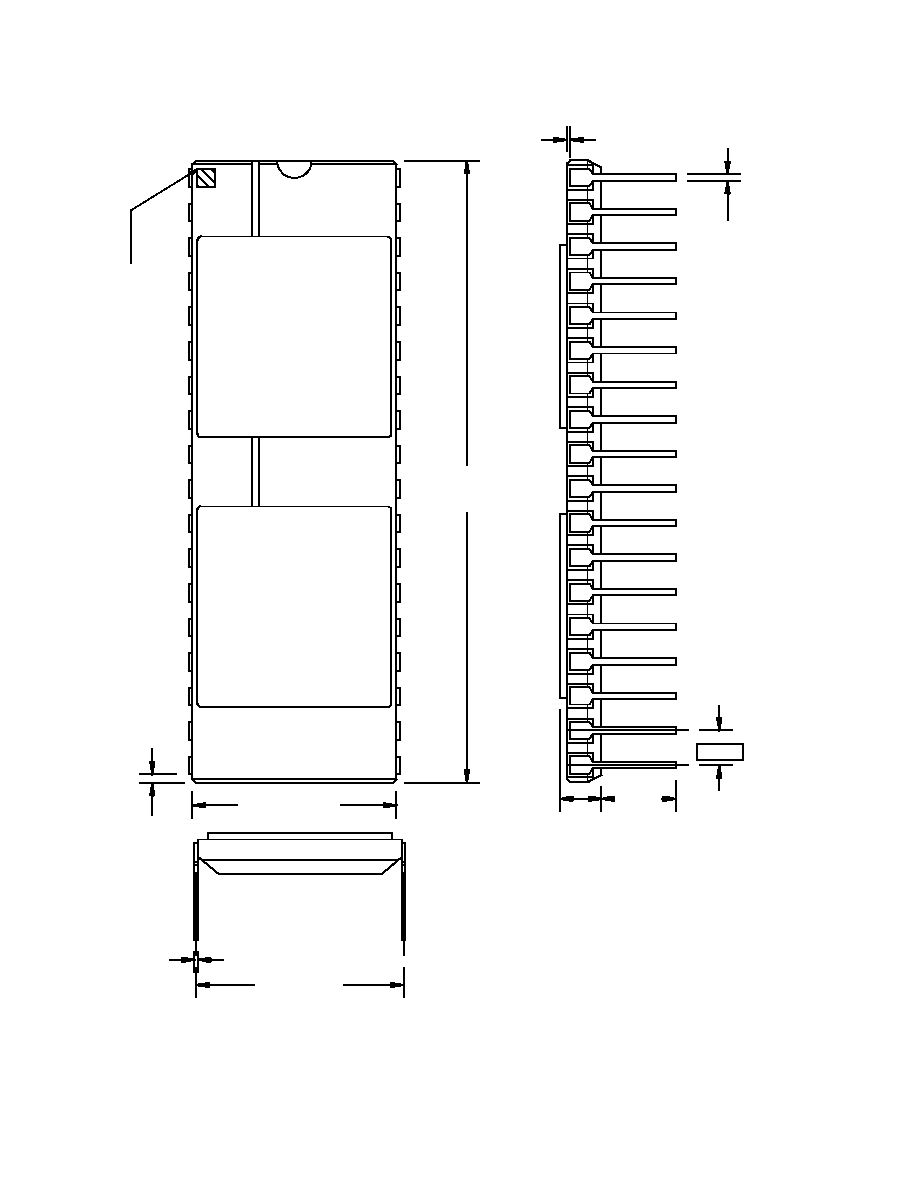
Figure 13. 24-Pin Side-Brazed DIP, Single Cavity
18
Notes:
1. All package finishes are per MIL-M-38510.
2. It is recommended that package ceramic be mounted on a heat removal
rail in the printed circuit board. A thermally conductive material such as
MERECO XLN-589 or equivalent should be used.
3. Letter designations are for cross-refernce to MIL-M-38510.
Figure 14. 36-Pin Lead Flatpack
(100-MIL Lead Spacing)

19
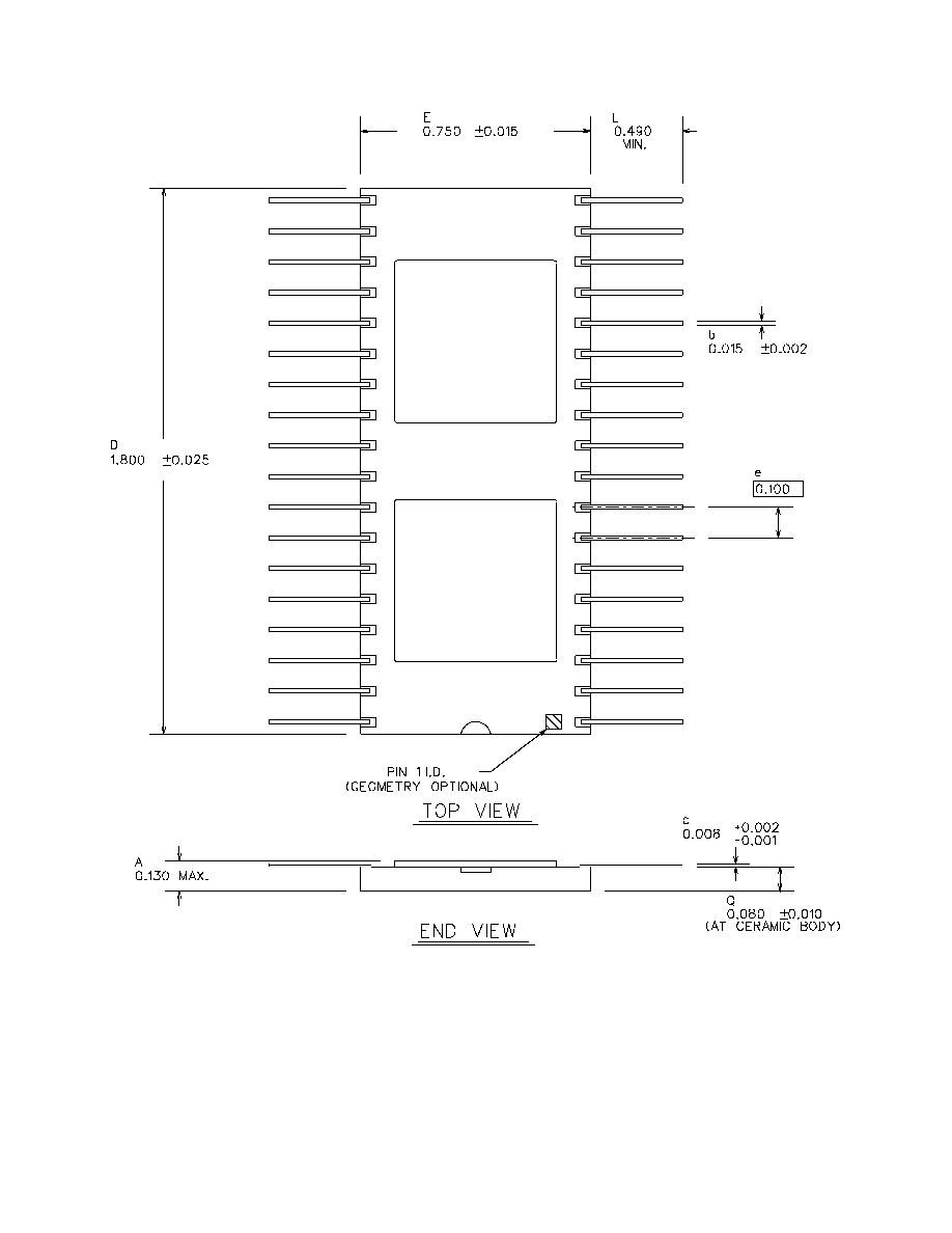
Figure 15. 36-Lead Flatpack, Dual Cavity
(50-Mil Lead Spacing)
Notes:
1. Package material: opaque ceramic.
2. All package plating finishes are per MIL-M-38510.
3. Lid is not connected to any electrical potential.
4. It is recommended that package ceramic be mounted to a heat removal rail located in the
printed circuit board. A thermally conductive material such as Mereco XLN-589 or
equivalent should be used.
1.00+.025
E
0.700
±
0.015
L
LEAD 1 INDICATOR
A
0.130 MAX.
Q
0.070
±
0.010
(AT CERAMIC BODY)
D
-
e
.050
b
0.016
±
.002
C
0.007 -0.001
+0.002

20
ORDERING INFORMATION
UT63M Single Channel MIL-STD-1553 Monolithic Transceiver: SM
Lead Finish:
(A) = Solder
(C) = Gold
(X) = Optional
Case Outline:
(U) = 24 pin DIP
Class Designator:
(-)
= Bland or No field is QML Q
(Q) = QML
Device Type
(01) = +\-15V, idle low
(02) = +\-12V, Idle low
Drawing Number: 88644
Total Dose: None
(R) = 1E5 (100KRad)
Federal Stock Class Designator: No options
5962 * * * * * *
Notes:
1. Lead finish (A, C, or X) must be specified.
2. If an "X" is specified when ordering, part marking will match the lead finish and will be either "A" (solder) or "C" (gold).
3. RadHard offered only on 01 device type. Cobalt 60testing required.
4. For QML Q product, the Q designator is intentionally left blank in the SMD number (e.g. 5962-8864401UX).

21
UT63M Single Channel MIL-STD-1553 Monolithic Transceiver
Radiation:
5 = 1E5 rads(Si)
- = None
Lead Finish:
(A) = Solder
(C) = Gold
(X) = Optional
Screening:
(C) = Military Temperature
(P) = Prototype
(Q) = QML-Q
(V) = QML-V
Package Type:
(P) = 24-pin DIP
Device Type Modifier:
105 = +\-15V, Idle low
107 = +\- 12V, Idle Low
UT63M * * * * *
Notes:
1. Lead finish (A, C, or X) must be specified.
2. If an "X" is specified when ordering, part marking will match the lead finish and will be either "A" (solder) or "C" (gold).
3. Military Temperature range devices are burned-in and are tested at -55
∞
C, room temperature, and 125
∞
C. Radiation characteristics are neither tested
nor guaranteed and may not be specified.
4. Devices have prototype assembly and are tested at 25
∞
C only. Radiation characteristics are neither tested nor guaranteed and may not be specified. Lead
finish is at UTMC's option and an "X" must be specified when ordering.
5. The 63M105 only may be ordered with 1E5 rads(Si) total dose. Co60 testing is required. Contact factory for details.
6. SEU and neutron irradiation limits will be added when available.

Appendix 1 - 22
ORDERING INFORMATION
UT63M Dual Monolithic Transceiver: SMD
Lead Finish:
(A) = Solder
(C) = Gold
(X) = Optional
Case Outline:
(X) = 36 pin DIP
(Y) = 36 pin FP (.100)
(Z ) = 36 pin FP (.50)
Class Designator:
(-)
= Blank orNo field is QML Q
(V) = QML V
Device Type
(05) = +\-15V, idle low
(06) = +\-12V, Idle low
Drawing Number: 88644
(-)
= None
(R) = 1E5 (100Krad)
Federal Stock Class Designator: No options
5962 * * * * *
Notes:
1. Lead finish (A, C, or X) must be specified.
2. If an "X" is specified when ordering, part marking will match the lead finish and will be either "A" (solder) or "C" (gold).
3. RadHard offered only on 05 device type. Cobalt 60testing required.
4. For QML Q product, the Q designator is intentionally left blank in the SMD number (e.g. 5962-8864405YX).

23
UT63M Dual Multichip Monolithic Transceiver
Radiation:
None
Lead Finish:
(A) = Solder
(C) = Gold
(X) = Optional
Screening:
(C) = Military Temperature
(P) = Prototype
(Q) = QML-Q
(V) = QML-V
Package Type:
(B) = 36-pin DIP
(D) = 36-pin FP (.100)
(C) = 36-pin FP (.50)
Device Type Modifier:
125 = +\-15V, Idle low
127 = +\- 12V, Idle Low
UT63M- * * * *
Notes:
1. Lead finish (A, C, or X) must be specified.
2. If an "X" is specified when ordering, part marking will match the lead finish and will be either "A" (solder) or "C" (gold).
3. Military Temperature range devices are burned-in and tested at -55
∞
C, room temperature, and 125
∞
C. Radiation characteristics are neither tested nor
guaranteed and may not be specified.
4. Devices have prototype assembly and are tested at 25
∞
C only. Radiation characteristics are neither tested nor guaranteed and may not be specified. Lead
finish is GOLD only.