 | –≠–ª–µ–∫—Ç—Ä–æ–Ω–Ω—ã–π –∫–æ–º–ø–æ–Ω–µ–Ω—Ç: UTI760A | –°–∫–∞—á–∞—Ç—å:  PDF PDF  ZIP ZIP |
RTS-1
UTI760A RTS Remote Terminal for Stores
F
EATURES
À
Complete MIL-STD-1760A Notice I through III
remote terminal interface
À
1K x 16 of on-chip static RAM for message data,
completely accessible to host
À
Self-test capability, including continuous loop-back
compare
À
Programmable memory mapping via pointers for
efficient use of internal memory, including buffering
multiple messages per subaddress
À
RT-RT Terminal Address Compare
À
Command word stored with incoming data for
enhanced data management
À
User selectable RAM Busy (RBUSY) signal for slow
or fast processor interfacing
À
Full military operating temperature range, -55
∞
C to
+125
∞
C, screened to the specific test methods listed in
Table I of MIL-STD-883, Method 5004, Class B, also
Standard Military Drawing available
À
Available in 68-pin pingrid array package
I
NTRODUCTION
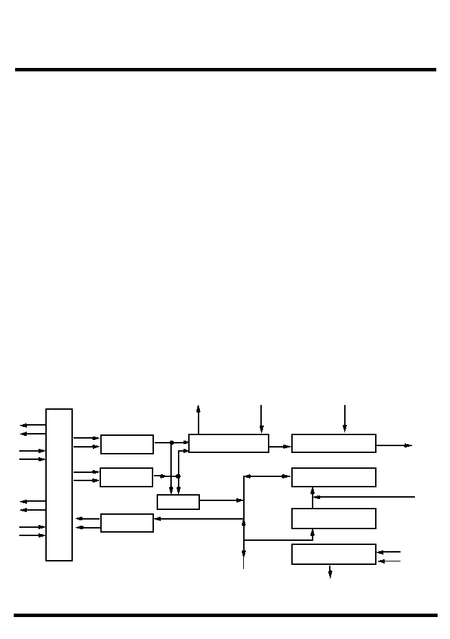
The UT1760A RTS is a monolithic CMOS VLSI solution
to the requirements of the dual-redundant MIL-STD-1553B
interface as specified by MIL-STD-1760A. Designed to
reduce cost and space in the mission stores interface, the
RTS integrates the remote terminal logic with a user-
configured 1K x 16 static RAM. In addition, the RTS has a
flexible subsystem interface to permit use with most
processors or controllers.
The RTS provides all protocol, data handling, error
checking, and memory control functions, as well as
comprehensive self-test capabilities. The RTS's memory
meets all of a mission store's message storage needs through
user-defined memory mapping. This memory-mapped
architecture allows multiple message buffering at
DECODER
COMMAND
RECOGNITION
DECODER
ENCODER
MUX
OUT
OUT
IN
IN
MCSA(4:0)
RTA(4:0)
REMOTE TERMINAL
ADDRESS
MODE CODE/
SUBADDRESS
CONTROL AND
ERROR LOGIC
CONTROL
INPUTS
STATUS
OUTPUTS
1K X 16 RAM
ADDR(9:0)
PTR REGISTER
DATA(15:0)
2MHz
12MHz
RESET
CLOCK AND RESET
LOGIC
Figure 1. UT1760A RTS Functional Block Diagram
OUTPUT MUL
TIPLEXING AND
SELF-TEST WRAP
AR
OUND
LOGIC

RTS-2
Table of Contents
1.0 ARCHITECTURE
AND
OPERATION
. . . . . . . . . . . . . . . . . . . . . . . . . . . . . . . . . .3
1.1
Memory Map and Host Memory Interface . . . . . . . . . . . . . . . . . . . . . . . . . . . 3
1.2
RTS RAM Pointer Structure . . . . . . . . . . . . . . . . . . . . . . . . . . . . . . . . . . . . . . 4
1.3
Internal Register Description . . . . . . . . . . . . . . . . . . . . . . . . . . . . . . . . . . . . . . 5
1.4
Mode Code and Subaddress . . . . . . . . . . . . . . . . . . . . . . . . . . . . . . . . . . . . . . . 8
1.5
MIL-STD-1760A Subaddress and Mode Code Definitions . . . . . . . . . . . . . . . 9
1.6
Terminal Address . . . . . . . . . . . . . . . . . . . . . . . . . . . . . . . . . . . . . . . . . . . . . . .12
1.7
Internal Self-Test . . . . . . . . . . . . . . . . . . . . . . . . . . . . . . . . . . . . . . . . . . . . . . .12
1.8
Power-up and Master Reset . . . . . . . . . . . . . . . . . . . . . . . . . . . . . . . . . . . . . . .12
1.9
Encoder and Decoder . . . . . . . . . . . . . . . . . . . . . . . . . . . . . . . . . . . . . . . . . . . .12
1.10
RT-RT Transfer Compare . . . . . . . . . . . . . . . . . . . . . . . . . . . . . . . . . . . . . . . . .12
1.11 Illegal Command Decoding . . . . . . . . . . . . . . . . . . . . . . . . . . . . . . . . . . . . . . .13
2.0
MEMORY MAP EXAMPLE
. . . . . . . . . . . . . . . . . . . . . . . . . . . . . . . . . . . . . . . . . .13
3.0
PIN IDENTIFICATION AND DESCRIPTION
. . . . . . . . . . . . . . . . . . . . . . . . . . .16
4.0
MAXIMUM AND RECOMMENDED OPERATING CONDITIONS
22
5.0
DC ELECTRICAL CHARACTERISTICS
. . . . . . . . . . . . . . . . . . . . . . . . . . . . . . .23
6.0
AC ELECTRICAL CHARACTERISTICS
. . . . . . . . . . . . . . . . . . . . . . . . . . . . . . .24
7.0
PACKAGE OUTLINE DRAWING
. . . . . . . . . . . . . . . . . . . . . . . . . . . . . . . . . . . . .35

RTS-3
1.0 A
RCHITECTURE
A
ND
O
PERATION
The UT1760A RTS is an interface device linking a MIL-
STD-1553 serial data bus and a host microprocessor system.
The RTS's MIL-STD-1553B interface includes encoding/
decoding logic, error detection, command recognition, 1K
x 16 of SRAM, pointer registers, clock, and reset circuits.
Illegal subaddress circuitry makes the RTS MIL-STD-
1760A-specific.
1.1 Memory Map and Host Memory Interface
The host can access the 1K x 16 RAM memory like a
standard RAM device through the 10-bit address and 16-bit
data buses. The host uses the Chip Select (CS), Read/Write
(RD/WR), and Output Enable (OE) signals to control data
transfer to and from memory. When the RTS requires access
to its own internal RAM, it asserts the RBUSY signal to
alert the host. The RBUSY signal is programmable via the
internal Control Register to be asserted either 5.7ms or
2.7ms prior to the RTS needing access to its internal RAM.
The RTS stores MIL-STD-1760A messages in 1K x 16 of
on-chip RAM. For efficient use of the 1K x 16 memory on
the RTS, the host programs a set of pointers to map where
the 1760A message is stored. The RTS uses the upper 64
words (address 3C0 (hex) through 3FF (hex)) as pointers.
The RTS provides pointers for all 30 receive subaddresses,
all 30 transmit subaddresses, and four mode code
commands with associated data words as defined in
MIL-STD-1553B. The remaining 960 words of memory
contain receive, transmit, and mode code data in a
host-defined structure.
Figure 2. RTS Memory Map
15 MSB
0 LSB
RTS Memory Map
3C0 (hex)
3DF (hex)
3C1 (hex)
3DE (hex)
RCV SUBADDRESS 01
RCV SUBADDRESS 30
XMIT VECTOR WORD MODE CODE (W/DATA)
SYNCHRONIZE MODE CODE (W/DATA)
15 MSB
0 LSB
3FF (hex)
XMIT LAST COMMAND MODE CODE (W/DATA)
XMT BIT WORD MODE CODE (W/DATA)
3E0 (hex)
XMT SUBADDRESS 30
3FE (hex)
3E1 (hex)
15 MSB
0 LSB
000 (hex)
3BF(hex)
Message
Storage
Locations
Receive
Message
Pointers
Transmit
Message
Pointers
(3C1 TO 3DE)
(3E1 TO 3FE)
XMT SUBADDRESS 01
RTS-4
1.2 RTS RAM Pointer Structure
The RAM 16-bit pointers have a 6-bit index field and a
10-bit address field. The 6-bit index field allows for the
storage of up to 64 messages per subaddress. A message
consists of the 1553 command word and its associated
data words.
The 16-bit pointer for Transmit Last Command Mode Code
is located at memory location 3E0 (hex). The Transmit Last
Command Mode Code pointer buffers up to 63 command
words. An example of command word storage follows:
Example:
3E0 (hex)
Contents = FC00 (hex)
11 1111 00 0000 0000
Address Field = 000 (hex)
Index Field = 3F (hex)
First command word storage location (3E0 = F801):
Address Field = 001 (hex)
Index Field = 3E (hex)
Sixty-third command word storage location
(3E0 = 003F):
Address Field = 03F (hex)
Index Field = 00 (hex)
Sixty-fourth command word storage location (3E0 = 003F)
(previous command word overwritten):
Address Field = 03F (hex)
Index Field = 00 (hex)
The Transmit Last Command Mode Code has Address Field
boundary conditions for the location of command word
buffers. The host can allocate a maximum 63 sequential
locations following the Address Field starting address. For
proper operation, the Address Field must start on an I x 40
(hex) address boundary, where I is greater than or equal to
zero and less than or equal to 14. A list of valid Index and
Address Fields follows:
Figure 3. Message Pointer Structure
MESSAGE INDEX
MESSAGE DATA ADDRESS
15 (MSB)
0 (LSB)
Message Index:
Defines the maximum
messages buffered for the
given subaddress.
Message Data Address:
Indicates the starting memory
address for incoming message
storage.
10
9
I
Valid Index Fields
Valid Address Fields
0
3F (hex) to 00 (hex)
000 (hex) to 03F(hex)
1
3F (hex) to 00 (hex)
040 (hex) to 07F (hex)
2
3F (hex) to 00 (hex)
080 (hex) to 0BF(hex)
3
3F (hex) to 00 (hex)
0C0 (hex) to 0FF (hex)
4
3F (hex) to 00 (hex)
100 (hex) to 13F (hex)
5
3F (hex) to 00 (hex)
140 (hex) to 17F (hex)
6
3F (hex) to 00 (hex)
180 (hex) to 1BF (hex)
7
3F (hex) to 00 (hex)
1C0 (hex) to 1FF (hex)
8
3F (hex) to 00 (hex)
200 (hex) to 23F (hex)
9
3F (hex) to 00 (hex)
240 (hex) to 27F (hex)
10
3F (hex) to 00 (hex)
280 (hex) to 2BF (hex)
11
3F (hex) to 00 (hex)
2C0 (hex) to 2FF (hex)
12
3F (hex) to 00 (hex)
300 (hex) to 33F (hex)
13
3F (hex) to 00 (hex)
340 (hex) to 37F (hex)
14
3F (hex) to 00 (hex)
380 (hex) to 3BF (hex)

RTS-5
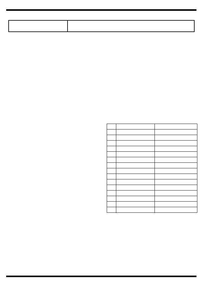
1.3 Internal Registers
The RTS uses two internal registers to allow the host to
control the RTS operation and monitor its status. The host
uses the Control (CTRL) signal along with Chip Select (CS),
Read/Write (RD/WR), and Output Enable (OE) to read the
16-bit Status Register or write to the 13-bit Control Register.
No address data is needed to select a register. The Control
Register toggles bits in the MIL-STD-1553B status word,
enables the biphase inputs, recognizes broadcast
commands, selects Notice I and II or III, determines RAM
Busy (RBUSY) timing, selects disconnect or terminal active
flag, and puts the part in self-test mode. The Status Register
supplies operational status of the UT1760A RTS to the host.
These registers must be initialized before attempting RTS
operation. Internal registers can be accessed while RBUSY
is active.
Subaddress/Mode Code
RAM Location
Subaddress/Mode Code
RAM Location
Transmit Vector Word Mode Code
3C0 (hex)
Transmit Last Command Mode Code
3E0 (hex)
Receive Subaddress
01
3C1 (hex)
Transmit Subaddress
01
3E1 (hex)
Receive Subaddress
02
3C2 (hex)
Transmit Subaddress
02
3E2 (hex)
Receive Subaddress
03
3C3 (hex)
Transmit Subaddress
03
3E3 (hex)
Receive Subaddress
04
3C4 (hex)
Transmit Subaddress
04
3E4 (hex)
Receive Subaddress
05
3C5 (hex)
Transmit Subaddress
05
3E5 (hex)
Receive Subaddress
06
3C6 (hex)
Transmit Subaddress
06
3E6 (hex)
Receive Subaddress
07
3C7 (hex)
Transmit Subaddress
07
3E7 (hex)
Receive Subaddress
08
3C8 (hex)
Transmit Subaddress
08
3E8 (hex)
Receive Subaddress
09
3C9 (hex)
Transmit Subaddress
09
3E9 (hex)
Receive Subaddress
10
3CA (hex)
Transmit Subaddress
10
3EA (hex)
Receive Subaddress
11
3CB (hex)
Transmit Subaddress
11
3EB (hex)
Receive Subaddress
12
3CC (hex)
Transmit Subaddress
12
3EC (hex)
Receive Subaddress
13
3CD (hex)
Transmit Subaddress
13
3ED (hex)
Receive Subaddress
14
3CE (hex)
Transmit Subaddress
14
3EE (hex)
Receive Subaddress
15
3CF (hex)
Transmit Subaddress
15
3EF (hex)
Receive Subaddress
16
3D0 (hex)
Transmit Subaddress
16
3F0 (hex)
Receive Subaddress
17
3D1 (hex)
Transmit Subaddress
17
3F1 (hex)
Receive Subaddress
18
3D2 (hex)
Transmit Subaddress
18
3F2 (hex)
Receive Subaddress
19
3D3 (hex)
Transmit Subaddress
19
3F3 (hex)
Receive Subaddress
20
3D4 (hex)
Transmit Subaddress
20
3F4 (hex)
Receive Subaddress
21
3D5 (hex)
Transmit Subaddress
21
3F5 (hex)
Receive Subaddress
22
3D6 (hex)
Transmit Subaddress
22
3F6 (hex)
Receive Subaddress
23
3D7 (hex)
Transmit Subaddress
23
3F7 (hex)
Receive Subaddress
24
3D8 (hex)
Transmit Subaddress
24
3F8 (hex)
Receive Subaddress
25
3D9 (hex)
Transmit Subaddress
25
3F9 (hex)
Receive Subaddress
26
3DA (hex)
Transmit Subaddress
26
3FA (hex)
Receive Subaddress
27
3DB (hex)
Transmit Subaddress
27
3FB (hex)
Receive Subaddress
28
3DC (hex)
Transmit Subaddress
28
3FC (hex)
Receive Subaddress
29
3DD (hex)
Transmit Subaddress
29
3FD (hex)
Receive Subaddress
30
3DE (hex)
Transmit Subaddress
30
3FE (hex)
Synchronize w/Data Word Mode Code
3DF (hex)
Transmit Bit Word Mode Code
3FF (hex)