 | –≠–ª–µ–∫—Ç—Ä–æ–Ω–Ω—ã–π –∫–æ–º–ø–æ–Ω–µ–Ω—Ç: W3150 | –°–∫–∞—á–∞—Ç—å:  PDF PDF  ZIP ZIP |

© Copyright 2005 WIZnet Co., Inc. All rights reserved.
…
…
Ì
Ì
Ô
Ô
Î
Î
Ð
Ð
ø
ø
¨
¨
ø
ø
-
-
∏
∏
ª
ª
ª
ª
¨
¨
¯
¯
ª
ª
Æ
Æ
Ú
Ú
Ô
Ô
Ú
Ú
˜
˜
ÒÎÁ
W
W
3
3
1
1
5
5
0
0
D
D
a
a
t
t
a
a
s
s
h
h
e
e
e
e
t
t
(Ver. 1.0)
©2005 WIZnet Co., Inc. All Rights Reserved.
For more information, visit our website at
http://www.wiznet.co.kr

…
…
Ì
Ì
Ô
Ô
Î
Î
Ð
Ð
ø
ø
¨
¨
ø
ø
-
-
∏
∏
ª
ª
ª
ª
¨
¨
¯
¯
ª
ª
Æ
Æ
Ú
Ú
Ô
Ô
Ú
Ú
˜
˜
Document History Information
Revision
Data
Description
Ver. 1.0
May 16, 2005
Release with W3150 Launching
© Copyright 2005 WIZnet Co., Inc. All rights reserved.
ÔÒÎÁ

WIZnet
'
s Online Technical Support
C
C
l
l
i
i
c
c
k
k

…
…
Ì
Ì
Ô
Ô
Î
Î
Ð
Ð
ø
ø
¨
¨
ø
ø
-
-
∏
∏
ª
ª
ª
ª
¨
¨
¯
¯
ª
ª
Æ
Æ
Ú
Ú
Ô
Ô
Ú
Ú
˜
˜
ÌÒÎÁ
iinChip
TM
W3150 Datasheet
Description
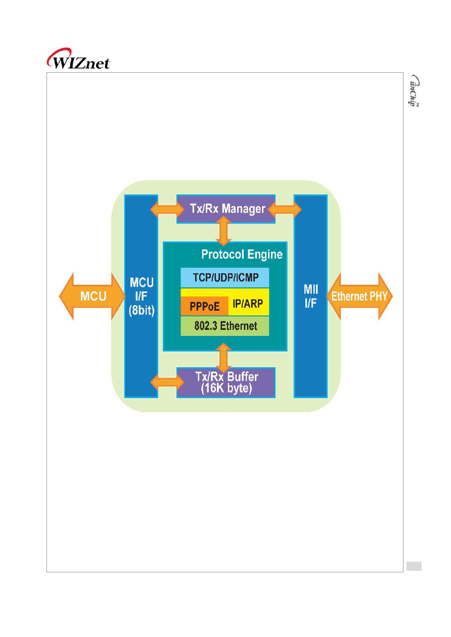
The iinChip W3150 is an LSI of hardware protocol stack that provides an easy, low-cost solution for high-
speed Internet connectivity for digital devices by allowing simple installation of TCP/IP stack in the hardware.
The W3150 offers system designers a quick, easy way to add Ethernet networking functionality to any
product. Implementing this LSI into a system can completely offload Internet connectivity and processing
standard protocols from the system, thereby significantly reducing the software development cost.
The W3150 contains TCP/IP Protocol Stacks such as TCP, UDP, ICMP, IPv4, ARP and PPPoE protocols, as
well as Ethernet protocols such as Data Link Control and MAC protocol. The total internal memory size is
16Kbytes, which is the buffer for transmit and receive operations.
The W3150 provides a local bus interface to various MCUs and standard MII(Media Independent Interface)
specification consisting of nibble data bus for Ethernet PHY devices.
The W3150 is a best-fitted device for embedded application with Internet-Connectivity including IP-Setop
Box, Internet-DVR, Internet phones, VoIP SOC chips, Internet MP3 players, handheld medical devices,
various industrial system monitoring and metering, and many other non-portable electronic devices such as
large consumer electronic products.
Features
Support Hardwired TCP/IP Protocols : TCP, UDP, ICMP, IPv4, ARP, PPPoE, Ethernet
Support PPPoE Protocol with PAP/CHAP Authentication mode
Supports 4 independent sockets simultaneously
Standard MII Interface for Ethernet-PHY chip
Supports 10BaseT/100BaseTX
Supports full-duplex mode
Internal 16Kbytes Memory for Tx/Rx Buffers
0.25 µm CMOS technology
3.3V operation with 5V I/O signal tolerance
Small 64 Pin LQFP Package
Lead-Free Package
Commercial Temperature Range from 0 C to 80 C
© Copyright 2005 WIZnet Co., Inc. All rights reserved.
…
…
Ì
Ì
Ô
Ô
Î
Î
Ð
Ð
ø
ø
¨
¨
ø
ø
-
-
∏
∏
ª
ª
ª
ª
¨
¨
¯
¯
ª
ª
Æ
Æ
Ú
Ú
Ô
Ô
Ú
Ú
˜
˜
ÏÒÎÁ
Block Diagram
© Copyright 2005 WIZnet Co., Inc. All rights reserved.

…
…
Ì
Ì
Ô
Ô
Î
Î
Ð
Ð
ø
ø
¨
¨
ø
ø
-
-
∏
∏
ª
ª
ª
ª
¨
¨
¯
¯
ª
ª
Æ
Æ
Ú
Ú
Ô
Ô
Ú
Ú
˜
˜
ÎÒÎÁ
Table of Contents
Description ...................................................................................................................3
Features ......................................................................................................................3
Block Diagram ...............................................................................................................4
Table of Contents............................................................................................................5
1.
Pin Assignment ........................................................................................................7
1.1.
MII Signal Description .....................................................................................8
1.2.
MCU Interface Signal Description .......................................................................9
1.3.
Miscellaneous Signal Description ..................................................................... 10
1.4.
Power Supply Signal Description ...................................................................... 11
2.
Memory map ......................................................................................................... 12
3.
W3150 Registers .................................................................................................... 13
3.1.
Common Registers ...................................................................................... 13
3.2.
Socket Registers ......................................................................................... 14
4.
Register Descriptions ............................................................................................... 18
4.1.
Common Registers ...................................................................................... 18
4.2.
Socket Registers ......................................................................................... 24
5.
Functional Description .............................................................................................. 32
5.1.
Initialization ............................................................................................... 32
5.2.
Data communication..................................................................................... 32
5.2.1.
TCP
5.2.2.
UDP
5.2.3.
IP raw
5.3.
Usage of PPPoE environment ......................................................................... 44
6.
Application Information ............................................................................................. 48
6.1.
Direct Bus I/F Mode...................................................................................... 48
6.2.
Indirect Bus I/F Mode.................................................................................... 48
6.3.
MII (Media Independent Interface) .................................................................... 49
7.
Electrical Specification .............................................................................................. 50
7.1.
Absolute Maximum Ratings ............................................................................ 50
7.2.
DC Characteristics ....................................................................................... 50
7.3.
AC Characteristics ....................................................................................... 51
7.3.1.
Reset Timing
7.3.2.
Register/Memory READ Timing
7.3.3.
Register/Memory WRITE Timing
7.3.4.
MII(Media Independent Interface) Timing
© Copyright 2005 WIZnet Co., Inc. All rights reserved.

…
…
Ì
Ì
Ô
Ô
Î
Î
Ð
Ð
ø
ø
¨
¨
ø
ø
-
-
∏
∏
ª
ª
ª
ª
¨
¨
¯
¯
ª
ª
Æ
Æ
Ú
Ú
Ô
Ô
Ú
Ú
˜
˜
ÍÒÎÁ
8.
IR Reflow Temperature Profile (Lead-Free)...................................................................... 56
9.
Package Description ................................................................................................ 57
© Copyright 2005 WIZnet Co., Inc. All rights reserved.

…
…
Ì
Ì
Ô
Ô
Î
Î
Ð
Ð
ø
ø
¨
¨
ø
ø
-
-
∏
∏
ª
ª
ª
ª
¨
¨
¯
¯
ª
ª
Æ
Æ
Ú
Ú
Ô
Ô
Ú
Ú
˜
˜
ÈÒÎÁ
1. Pin Assignment
/
C
S
/
R
D
/
W
R
/
I
N
T
N
C
N
C
V
C
C
V
O
U
T
T
E
S
T
T
X
C
G
N
D
T
X
E
N
T
X
D
[
3
]
T
X
D
[
2
]
T
X
D
[
1
]
T
X
D
[
0
]
64
63
62
61
60
59
58
57
56
55
54
53
52
51
50
49
/RESET
1
48
COL
VCC
2
47
CRS
GND
3
46
RXC
TEST
4
45
GND
A[14]
5
44
RXDV
A[13]
6
43
RXD[3]
A[12]
7
42
RXD[2]
A[11]
8
W3150
41
RXD[1]
A[10]
9
40
RXD[0]
A[9]
10
39
VCC
A[8]
11
38
VCC
TEST
12
37
AVIN
GND
13
36
GND
A[7]
14
35
CLOCK
A[6]
15
34
/FDPLX
A[5]
16
64 LQFP
33
PLOCK
17
18
19
20
21
22
23
24
25
26
27
28
29
30
31
32
A
[
4
]
A
[
3
]
A
[
2
]
A
[
1
]
A
[
0
]
V
C
C
G
N
D
D
[
7
]
D
[
6
]
D
[
5
]
D
[
4
]
V
I
N
D
[
3
]
D
[
2
]
D
[
1
]
D
[
0
]
© Copyright 2005 WIZnet Co., Inc. All rights reserved.

…
…
Ì
Ì
Ô
Ô
Î
Î
Ð
Ð
ø
ø
¨
¨
ø
ø
-
-
∏
∏
ª
ª
ª
ª
¨
¨
¯
¯
ª
ª
Æ
Æ
Ú
Ú
Ô
Ô
Ú
Ú
˜
˜
ËÒÎÁ
1.1.MII Signal Description
Pin#
Signal
I/O
Description
55
TXC
I
Transmit Clock
This pin provides a continuous clock as a timing reference for TXD[3:0] and
TXEN. TXC is sourced by the PHY. TXC is 2.5 MHz in 10BASET Nibble
mode, and 25 MHz in 100BASETX Nibble mode.
53
TXEN
O
Transmit Enable
This output signal indicates the presence of a valid nibble data on TXD[3:0]. It
becomes active when the first nibble data of the packet is valid on TXD[3:0]
and goes low after the last nibble data of the packet is clocked out of
TXD[3:0]. This signal connects directly to the PHY device. This signal is active
high.
52
51
50
49
TXD[3]
TXD[2]
TXD[1]
TXD[0]
O
Transmit Data
These pins provide Nibble NRZ data to the PHY synchronously with TXC
when TXEN is asserted.
46
RXC
I
Receive Clock
This pin provides a continuous clock reference for RXDV and RXD[3:0]
signals. RXC is sourced by the PHY. RXC is 2.5 MHz in 10BASET Nibble
mode, and 25 MHz in 100BASETX Nibble mode.
48
COL
I
Collision Detect
This pin becomes active when a collision has been detected in Half Duplex
modes. This signal is asynchronous, active high and ignored during full-
duplex operation. This signal is active high.
47
CRS
I
Carrier Sense
This pin indicates that carrier is present. This signal is active high.
44
RXDV
I
Receive Data Valid
This signal is asserted high when received data is present on the RXD[3:0]
pins; the signal is deasserted at the end of the packet. The signal is valid on
the rising of the RXC.
43
42
41
40
RXD[3]
RXD[2]
RXD[1]
RXD[0]
I
Receive Data
These pins receive Nibble NRZ data from the PHY device synchronously with
RXC when RXDV is asserted.
© Copyright 2005 WIZnet Co., Inc. All rights reserved.

…
…
Ì
Ì
Ô
Ô
Î
Î
Ð
Ð
ø
ø
¨
¨
ø
ø
-
-
∏
∏
ª
ª
ª
ª
¨
¨
¯
¯
ª
ª
Æ
Æ
Ú
Ú
Ô
Ô
Ú
Ú
˜
˜
ÁÒÎÁ
1.2.MCU Interface Signal Description
Pin#
Signal
I/O
Description
1
/RESET
I
RESET
Active Low input that initializes or re-initializes W3150.
Asserting this pin low for at least 125us will force a reset process to occur
which will result in all internal registers re-initializing to their default states.
35
CLOCK
I
CLOCK
This pin is the Primary clock required for internal operation of W3150. In
general, PHY driving clock can be shared for saving cost. 25MHz is required.
Note) Sharing crystal source clock with multiple devices may cause some
troubles. In our reference design, we used one crystal for both PHY and
W3150 with verification.
But for other kind of PHY, please confirm safety prior to decision.
5:11
14:21
A[14:8]
A[7:0]
I
ADDRESS PINS
These pins are used to select a register or memory.
24:27,
29:32
D[7:4]
D[3:0]
I/O
DATA PINS
These pins are used to read and write register or memory data.
61
/INT
O
INTERRUPT
This pin Indicates that W3150 requires MCU attention after socket
connecting, disconnecting, receiving data or timeout. The interrupt is cleared
by reading IR(Interrupt Register) or S
n
_IR (Socket
n
th Interrupt Register). All
interrupts are maskable. This signal is active low.
64
/CS
I
CHIP SELECT
Chip Select places for MCU access to internal registers/memory. /WR and
/RD select direction of data transfer. This signal is active low.
62
/WR
I
WRITE ENABLE
Strobe from MCU to write an internal register/memory selected by A[14:0].
Data is latched into the W3150 on the rising edge of this input. This signal is
active low.
63
/RD
I
READ ENABLE
Strobe from MCU to read an internal register/memory selected by A[14:0].
This signal is active low.
© Copyright 2005 WIZnet Co., Inc. All rights reserved.

…
…
Ì
Ì
Ô
Ô
Î
Î
Ð
Ð
ø
ø
¨
¨
ø
ø
-
-
∏
∏
ª
ª
ª
ª
¨
¨
¯
¯
ª
ª
Æ
Æ
Ú
Ú
Ô
Ô
Ú
Ú
˜
˜
ÔÒÎÁ
1.3.Miscellaneous Signal Description
Pin#
Signal
I/O
Description
34
/FDPLX
I
FULL/HALF DUPLEX SELECT
This pin selects Half/Full Duplex operation.
This pin must be externally pulled low (typically x k ) in order to configure the
W3150 for Full Duplex operation.
Low = Full Duplex
High = Half Duplex
33
PLOCK
O
PLL Lock
Internal PLL Lock detector out. When the lock signal is High, W3150 is ready
to start. The lock signal always low when the PLL is in setting time. This signal
is active high.
4,12,56
TEST
I
FACTORY TEST INPUT
Used to check the chip's internal functions. This should be tied low during
normal operation.
59, 60
NC
© Copyright 2005 WIZnet Co., Inc. All rights reserved.

…
…
Ì
Ì
Ô
Ô
Î
Î
Ð
Ð
ø
ø
¨
¨
ø
ø
-
-
∏
∏
ª
ª
ª
ª
¨
¨
¯
¯
ª
ª
Æ
Æ
Ú
Ú
Ô
Ô
Ú
Ú
˜
˜
ÔÔÒÎÁ
1.4.Power Supply Signal Description
Pin#
Signal
I/O
Description
2, 22, 38, 39, 58
VCC
POSITIVE 3.3V SUPPLY PINS
28
VIN
2.5V power input
2.5V power supply
37
AVIN
2.5V Analog power input
2.5V power supply for analog circuit ; should be well decoupled.
Refer Figure 1-1. Reference Schematic for Power input.
57
VOUT
2.5V power out
Be sure to connect 10uF tantalum capacitor and a 0.1uF
capacitor for noise de-coupling. Then connect this pin through a
ferrite bead to VIN and AVIN.
3, 13, 23, 36, 45, 54
GND
NEGATIVE (GROUND) SUPPLY PINS
VOUT
AVIN
VIN
+
CP2
10uF
L3
4.7uH
C22
0.1uF
+
CP3
2.2uF
C21
0.1uF
Figure 1-1. Reference Schematic for Power input
© Copyright 2005 WIZnet Co., Inc. All rights reserved.

…
…
Ì
Ì
Ô
Ô
Î
Î
Ð
Ð
ø
ø
¨
¨
ø
ø
-
-
∏
∏
ª
ª
ª
ª
¨
¨
¯
¯
ª
ª
Æ
Æ
Ú
Ú
Ô
Ô
Ú
Ú
˜
˜
ÔÓÒÎÁ
2. Memory map
W3150 is composed of Common Register, Socket Register, TX Memory, and RX Memory. Each fields are
shown as below.
0x0000
Common Registers
0x0030
Not Used
0x0400
Socket Registers
0x0800
Not Used
0x6000
TX memory
0x8000
0xA000
RX memory
© Copyright 2005 WIZnet Co., Inc. All rights reserved.

…
…
Ì
Ì
Ô
Ô
Î
Î
Ð
Ð
ø
ø
¨
¨
ø
ø
-
-
∏
∏
ª
ª
ª
ª
¨
¨
¯
¯
ª
ª
Æ
Æ
Ú
Ú
Ô
Ô
Ú
Ú
˜
˜
ÔÌÒÎÁ
3. W3150 Registers
3.1. Common Registers
Address
Register
0x0000
Mode (MR)
0x0001
0x0002
0x0003
0x0004
Gateway Address
(GAR0)
(GAR1)
(GAR2)
(GAR3)
0x0005
0x0006
0x0007
0x0008
Subnet mask Address
(SUBR0)
(SUBR1)
(SUBR2)
(SUBR3)
0x0009
0x000A
0x000B
0x000C
0x000D
0x000E
Source Hardware Address
(SHAR0)
(SHAR1)
(SHAR2)
(SHAR3)
(SHAR4)
(SHAR5)
0x000F
0x0010
0x0011
0x0012
Source IP Address
(SIPR0)
(SIPR1)
(SIPR2)
(SIPR3)
0x0013
Type Of Service of IP (TOSR)
0x0014
Time To Live of IP (TTLR)
0x0015
Interrupt (IR)
0x0016
Interrupt Mask (IMR)
0x0017
0x0018
Retry Time
(RTR0)
(RTR1)
0x0019
Retry Count (RCR)
Address
Register
0x001A
RX Memory Size (RMSR)
0x001B
TX Memory Size (TMSR)
0x001C
0x001D
Authentication Type in PPPoE
(PATR0)
(PATR1)
0x001E
~
0x0029
Reserved
0x002A
0x002B
0x002C
0x002D
Unreachable IP Address
(UIPR0)
(UIPR1)
(UIPR2)
(UIPR3)
0x002E
0x002F
Unreachable Port
(UPORT0)
(UPORT1)
0x0030
~
0x03FF
Reserved
© Copyright 2005 WIZnet Co., Inc. All rights reserved.

…
…
Ì
Ì
Ô
Ô
Î
Î
Ð
Ð
ø
ø
¨
¨
ø
ø
-
-
∏
∏
ª
ª
ª
ª
¨
¨
¯
¯
ª
ª
Æ
Æ
Ú
Ú
Ô
Ô
Ú
Ú
˜
˜
ÔÏÒÎÁ
3.2. Socket Registers
Address
Register
0x0400
Socket 0 Mode (S0_MR)
0x0401
Socket 0 Command (S0_CR)
0x0402
Socket 0 Interrupt (S0_IR)
0x0403
Socket 0 Socket Status (S0_SSR)
0x0404
0x0405
Socket 0 Source Port
(S0_PORT0)
(S0_PORT1)
0x0406
0x0407
0x0408
0x0409
0x040A
0x040B
Socket 0 Destination Hardware Address
(S0_DHAR0)
(S0_DHAR1)
(S0_DHAR2)
(S0_DHAR3)
(S0_DHAR4)
(S0_DHAR5)
0x040C
0x040D
0x040E
0x040F
Socket 0 Destination IP Address
(S0_DIPR0)
(S0_DIPR1)
(S0_DIPR2)
(S0_DIPR3)
0x0410
0x0411
Socket 0 Destination Port
(S0_DPORT0)
(S0_DPORT1)
0x0412
0x0413
Socket 0 Maximum Segment Size
(S0_MSSR0)
(S0_MSSR1)
0x0414
Socket 0 Protocol in IP Raw mode
(S0_PROTO)
Address
Register
0x0415
~
0x041F
Reserved
0x0420
0x0421
Socket 0 TX Free Size
(S0_TX_FSR0)
(S0_TX_FSR1)
0x0422
0x0423
Socket 0 TX Read Pointer
(S0_TX_RR0)
(S0_TX_RR1)
0x0424
0x0425
Socket 0 TX Write Pointer
(S0_TX_WR0)
(S0_TX_WR1)
0x0426
0x0427
Socket 0 RX Received Size
(S0_RX_RSR0)
(S0_RX_RSR0)
0x0428
0x0429
Socket 0 RX Read Pointer
(S0_RX_RR0)
(S0_RX_RR1)
0x042A
0x042B
Socket 0 RX Write Pointer
(S0_RX_WR0)
(S0_RX_WR1)
0x042C
~
0x04FF
Reserved
© Copyright 2005 WIZnet Co., Inc. All rights reserved.

…
…
Ì
Ì
Ô
Ô
Î
Î
Ð
Ð
ø
ø
¨
¨
ø
ø
-
-
∏
∏
ª
ª
ª
ª
¨
¨
¯
¯
ª
ª
Æ
Æ
Ú
Ú
Ô
Ô
Ú
Ú
˜
˜
ÔÎÒÎÁ
Address
Register
0x0500
Socket 1 Mode (S1_MR)
0x0501
Socket 1 Command (S1_CR)
0x0502
Socket 1 Interrupt (S1_IR)
0x0503
Socket 1 Socket Status (S1_SSR)
0x0504
0x0505
Socket 1 Source Port
(S1_PORT0)
(S1_PORT1)
0x0506
0x0507
0x0508
0x0509
0x050A
0x050B
Socket 1 Destination Hardware Address
(S1_DHAR0)
(S1_DHAR1)
(S1_DHAR2)
(S1_DHAR3)
(S1_DHAR4)
(S1_DHAR5)
0x050C
0x050D
0x050E
0x050F
Socket 1 Destination IP Address
(S1_DIPR0)
(S1_DIPR1)
(S1_DIPR2)
(S1_DIPR3)
0x0510
0x0511
Socket 1 Destination Port
(S1_DPORT0)
(S1_DPORT1)
0x0512
0x0513
Socket 1 Maximum Segment Size
(S1_MSSR0)
(S1_MSSR1)
0x0514
Socket 1 Protocol in IP Raw mode
(S1_PROTO)
Address
Register
0x0515
~
0x051F
Reserved
0x0520
0x0521
Socket 1 TX Free Size
(S1_TX_FSR0)
(S1_TX_FSR1)
0x0522
0x0523
Socket 1 TX Read Pointer
(S1_TX_RR0)
(S1_TX_RR1)
0x0524
0x0525
Socket 1 TX Write Pointer
(S1_TX_WR0)
(S1_TX_WR1)
0x0526
0x0527
Socket 1 RX Received Size
(S1_RX_RSR0)
(S1_RX_RSR0)
0x0528
0x0529
Socket 1 RX Read Pointer
(S1_RX_RR0)
(S1_RX_RR1)
0x052A
0x052B
Socket 1 RX Write Pointer
(S1_RX_WR0)
(S1_RX_WR1)
0x052C
~
0x05FF
Reserved
© Copyright 2005 WIZnet Co., Inc. All rights reserved.

…
…
Ì
Ì
Ô
Ô
Î
Î
Ð
Ð
ø
ø
¨
¨
ø
ø
-
-
∏
∏
ª
ª
ª
ª
¨
¨
¯
¯
ª
ª
Æ
Æ
Ú
Ú
Ô
Ô
Ú
Ú
˜
˜
ÔÍÒÎÁ
Address
Register
0x0600
Socket 2 Mode (S2_MR)
0x0601
Socket 2 Command (S2_CR)
0x0602
Socket 2 Interrupt (S2_IR)
0x0603
Socket 2 Socket Status (S2_SSR)
0x0604
0x0605
Socket 2 Source Port
(S2_PORT0)
(S2_PORT1)
0x0606
0x0607
0x0608
0x0609
0x060A
0x060B
Socket 2 Destination Hardware Address
(S2_DHAR0)
(S2_DHAR1)
(S2_DHAR2)
(S2_DHAR3)
(S2_DHAR4)
(S2_DHAR5)
0x060C
0x060D
0x060E
0x060F
Socket 2 Destination IP Address
(S2_DIPR0)
(S2_DIPR1)
(S2_DIPR2)
(S2_DIPR3)
0x0610
0x0611
Socket 2 Destination Port
(S2_DPORT0)
(S2_DPORT1)
0x0612
0x0613
Socket 2 Maximum Segment Size
(S2_MSSR0)
(S2_MSSR1)
0x0614
Socket 2 Protocol in IP Raw mode
(S2_PROTO)
Address
Register
0x0615
~
0x061F
Reserved
0x0620
0x0621
Socket 2 TX Free Size
(S2_TX_FSR0)
(S2_TX_FSR1)
0x0622
0x0623
Socket 2 TX Read Pointer
(S2_TX_RR0)
(S2_TX_RR1)
0x0624
0x0625
Socket 2 TX Write Pointer
(S2_TX_WR0)
(S2_TX_WR1)
0x0626
0x0627
Socket 2 RX Received Size
(S2_RX_RSR0)
(S2_RX_RSR0)
0x0628
0x0629
Socket 2 RX Read Pointer
(S2_RX_RR0)
(S2_RX_RR1)
0x062A
0x062B
Socket 2 RX Write Pointer
(S2_RX_WR0)
(S2_RX_WR1)
0x062C
~
0x06FF
Reserved
© Copyright 2005 WIZnet Co., Inc. All rights reserved.

…
…
Ì
Ì
Ô
Ô
Î
Î
Ð
Ð
ø
ø
¨
¨
ø
ø
-
-
∏
∏
ª
ª
ª
ª
¨
¨
¯
¯
ª
ª
Æ
Æ
Ú
Ú
Ô
Ô
Ú
Ú
˜
˜
ÔÈÒÎÁ
Address
Register
0x0700
Socket 3 Mode (S3_MR)
0x0701
Socket 3 Command (S3_CR)
0x0702
Socket 3 Interrupt (S3_IR)
0x0703
Socket 3 Socket Status (S3_SSR)
0x0704
0x0705
Socket 3 Source Port
(S3_PORT0)
(S3_PORT1)
0x0706
0x0707
0x0708
0x0709
0x070A
0x070B
Socket 3 Destination Hardware Address
(S3_DHAR0)
(S3_DHAR1)
(S3_DHAR2)
(S3_DHAR3)
(S3_DHAR4)
(S3_DHAR5)
0x070C
0x070D
0x070E
0x070F
Socket 3 Destination IP Address
(S3_DIPR0)
(S3_DIPR1)
(S3_DIPR2)
(S3_DIPR3)
0x0710
0x0711
Socket 3 Destination Port
(S3_DPORT0)
(S3_DPORT1)
0x0712
0x0713
Socket 3 Maximum Segment Size
(S3_MSSR0)
(S3_MSSR1)
0x0714
Socket 3 Protocol in IP Raw mode
(S3_PROTO)
Address
Register
0x0715
~
0x071F
Reserved
0x0720
0x0721
Socket 3 TX Free Size
(S3_TX_FSR0)
(S3_TX_FSR1)
0x0722
0x0723
Socket 3 TX Read Pointer
(S3_TX_RR0)
(S3_TX_RR1)
0x0724
0x0725
Socket 3 TX Write Pointer
(S3_TX_WR0)
(S3_TX_WR1)
0x0726
0x0727
Socket 3 RX Received Size
(S3_RX_RSR0)
(S3_RX_RSR0)
0x0728
0x0729
Socket 3 RX Read Pointer
(S3_RX_RR0)
(S3_RX_RR1)
0x072A
0x072B
Socket 3 RX Write Pointer
(S3_RX_WR0)
(S3_RX_WR1)
0x072C
~
0x07FF
Reserved
© Copyright 2005 WIZnet Co., Inc. All rights reserved.

…
…
Ì
Ì
Ô
Ô
Î
Î
Ð
Ð
ø
ø
¨
¨
ø
ø
-
-
∏
∏
ª
ª
ª
ª
¨
¨
¯
¯
ª
ª
Æ
Æ
Ú
Ú
Ô
Ô
Ú
Ú
˜
˜
ÔËÒÎÁ
4. Register Descriptions
4.1. Common Registers
MR (Mode Register) [R/W] [0x0000] [0x00]
1
This Register is used for S/W Reset, memory test mode, ping block mode, PPPoE mode and Indirect bus I/F.
7
6
5
4
3
2
1
0
RST
MT
PB
PPPoE
LB
AI
IND
Bit
Symbol
Description
7
RST
S/W Reset
If this bit is 1, internal register will be initialized. It will be automatically cleared with
Reset.
6
Reserved
Reserved
5
MT
Memory Test Mode
0 : Disable memory test mode
1 : Enable memory test mode
TX memory is used for data transmission. In this memory, only WRITE can be performed.
At the RX memory, users can receive data and only READ can be performed. If a user
wants to perform both of WRITE and READ in order to check operation status of TX
memory and RX memory, the bit should be set as 1. Memory Test Mode is used only for
checking of TX/RX memory operation status. For the general usage, Memory Test Mode
should be cleared first.
4
PB
Ping Block Mode
0 : Disable Ping block
1 : Enable Ping block
If the bit is set as 1, there is no response to the Ping request.
3
PPPoE
PPPoE Mode
0 : Disable PPPoE mode
1 : Enable PPPoE mode
If you are under the circumstance of PPPoE such as ADSL, you should set the bit as 1,
and connect to PPPoE SERVER. For more detail, refer to 5.3 Usage of PPPoE SERVER.
1
[Read/Write] [Address] [Reset value]
© Copyright 2005 WIZnet Co., Inc. All rights reserved.

…
…
Ì
Ì
Ô
Ô
Î
Î
Ð
Ð
ø
ø
¨
¨
ø
ø
-
-
∏
∏
ª
ª
ª
ª
¨
¨
¯
¯
ª
ª
Æ
Æ
Ú
Ú
Ô
Ô
Ú
Ú
˜
˜
ÔÁÒÎÁ
2
LB
Little-endian / Big-endian ordering in Indirect Bus I/F
0 : Big-endian ordering
1 : Little-endian ordering
At the Indirect Bus I/F mode, Indirect address Register ordering is decided. For more
detail, refer to 6.1.2.Indirect Bus IF Mode.
1
AI
Address Auto-Increment in Indirect Bus I/F
0 : Disable auto-increment
1 : Enable auto-increment
At the Indirect Bus I/F mode, if this bit is set as 1, the address will automatically increase
by 1 whenever Read and Write are performed. For more detail, refer to 6.1.2 Indirect Bus
IF Mode.
0
IND
Indirect Bus I/F mode
0 : Disable Indirect bus I/F mode
1 : Enable Indirect bus I/F mode
If this bit is set as 1, Indirect Bis I/F mode is used. For more detail, refer to 6. Application
Information, 6.1.2. Indirect Bus IF Mode.
GWR (Gateway IP Address Register) [R/W] [0x0001
≠
0x0004] [0x00]
This Register sets up the default gateway address.
Ex) in case of 192.168.0.1
0x0001
0x0002
0x0003
0x0004
192 (0xC0)
168 (0xA8)
0 (0x00)
1 (0x01)
SUBR (Subnet Mask Register) [R/W] [0x0005
≠
0x0008] [0x00]
This Register sets up the subnet mask address.
Ex) in case of 255.255.255.0
0x0005
0x0006
0x0007
0x0008
255 (0xFF)
255 (0xFF)
255 (0xFF)
0 (0x00)
© Copyright 2005 WIZnet Co., Inc. All rights reserved.

…
…
Ì
Ì
Ô
Ô
Î
Î
Ð
Ð
ø
ø
¨
¨
ø
ø
-
-
∏
∏
ª
ª
ª
ª
¨
¨
¯
¯
ª
ª
Æ
Æ
Ú
Ú
Ô
Ô
Ú
Ú
˜
˜
ÓÒÎÁ
SHAR (Source Hardware Address Register) [R/W] [0x0009
≠
0x000E] [0x00]
This Register sets up the Source Hardware address.
Ex) In case of 00.08.DC.01.02.03
0x0009
0x000A
0x000B
0x000C
0x000D
0x000E
0x00
0x08
0xDC
0x01
0x02
0x03
SIPR (Source IP Address Register) [R/W] [0x000F
≠
0x0012] [0x00]
This Register sets up the Source IP address.
Ex) in case of 192.168.0.3
0x000F
0x0010
0x0011
0x0012
192 (0xC0)
168 (0xA8)
0 (0x00)
3 (0x03)
TOS (IP Type Of Service Register) [R/W] [0x0013] [0x00]
This Register sets up at the TOS Field of IP Header.
TTL (IP Time To Live Register) [R/W] [0x0014] [0x80]
This Register sets up at the TTL Field of IP Header.
IR (Interrupt Register) [R] [0x0015] [0x00]
This Register is accessed by the host processor to know the cause of an interrupt.
Any interrupt can be masked in the Interrupt Mask Register (IMR). The /INT signal retain low as long as any
unmasked signal is set, and will not go high until all unmasked bits in this Register have been cleared.
7
6
5
4
3
2
1
0
CONFLICT
UNREACH
PPPoE
Reserved
S3_INT
S2_INT
S1_INT
S0_INT
Bit
Symbol
Description
7
CONFLICT
IP Conflict
It is set as 1, when there is ARP request with same IP address as Source IP address.
This bit is cleared to 0 only with Read action.
6
UNREACH
Destination unreachable
W3150 will receive ICMP(Destination Unreachable) packet if not-existing Destination IP
address is transmitted during UDP data transmission. (Refer to 5.2.2. UDP). In this case,
the IP address and Port number will be saved in Unreachable IP Address (UIPR) and
Unreachable Port Register (UPORT), and the bit will be set as 1. This bit will be cleared
to 0 only with Read action.
© Copyright 2005 WIZnet Co., Inc. All rights reserved.

…
…
Ì
Ì
Ô
Ô
Î
Î
Ð
Ð
ø
ø
¨
¨
ø
ø
-
-
∏
∏
ª
ª
ª
ª
¨
¨
¯
¯
ª
ª
Æ
Æ
Ú
Ú
Ô
Ô
Ú
Ú
˜
˜
ÓÔÒÎÁ
5
PPPoE
PPPoE Close
In the PPPoE Mode, if the PPPoE connection is closed, 1 is set. This bit will be cleared
to 0 only with Read action.
4
Reserved
Reserved
3
S3_INT
Occurrence of Socket 3 Socket Interrupt
It is set in case that interrupt occurs at the socket 3. For more detailed information of
socket interrupt, refer to Socket 3 Interrupt Register(S3_IR). This bit will be automatically
cleared when S3_IR is cleared to 0x00.
2
S2_INT
Occurrence of Socket 2 Socket Interrupt
It is set in case that interrupt occurs at the socket 2. For more detailed information of
socket interrupt, refer to Socket 2 Interrupt Register(S2_IR). This bit will be automatically
cleared when S2_IR is cleared to 0x00.
1
S1_INT
Occurrence of Socket 1 Socket Interrupt
It is set in case that interrupt occurs at the socket 1. For more detailed information of
socket interrupt, refer to Socket 1 Interrupt Register(S1_IR). This bit will be automatically
cleared when S1_IR is cleared to 0x00.
0
S0_INT
Occurrence of Socket 0 Socket Interrupt
It is set in case that interrupt occurs at the socket 0. For more detailed information of
socket interrupt, refer to Socket 0 Interrupt Register(S0_IR). This bit will be automatically
cleared when S0_IR is cleared to 0x00.
IMR (Interrupt Mask Register) [R/W] [0x0016] [0x00]
The Interrupt Mask Register is used to mask interrupts. Each interrupt mask bit corresponds to a bit in the
Interrupt Register (IR). If an interrupt mask bit is set, an interrupt will be issued whenever the corresponding
bit in the IR is set. If any bit in the IMR is set as 0, an interrupt will not occur though the bit in the IR is set.
7
6
5
4
3
2
1
0
IM_IR7
IM_IR6
IM_IR5
Reserved
IM_IR3
IM_IR2
IM_IR1
IM_IR0
Bit
Symbol
Description
7
IM_IR7
IP Conflict Enable
6
IM_IR6
Destination unreachable Enable
5
IM_IR5
PPPoE Close Enable
4
Reserved
It should be set as
`
0
'
3
IM_IR3
Occurrence of Socket 3 Socket Interrupt Enable
2
IM_IR2
Occurrence of Socket 2 Socket Interrupt Enable
1
IM_IR1
Occurrence of Socket 1 Socket Interrupt Enable
© Copyright 2005 WIZnet Co., Inc. All rights reserved.
…
…
Ì
Ì
Ô
Ô
Î
Î
Ð
Ð
ø
ø
¨
¨
ø
ø
-
-
∏
∏
ª
ª
ª
ª
¨
¨
¯
¯
ª
ª
Æ
Æ
Ú
Ú
Ô
Ô
Ú
Ú
˜
˜
ÓÓÒÎÁ
0
IM_IR0
Occurrence of Socket 0 Socket Interrupt Enable
RTR (Retry Time-value Register) [R/W] [0x0017
≠
0x0018] [0x07D0]
This register sets the period of timeout. Vaule 1 means 100us. The initial value is 2000(0x07D0). That will be
set as 200ms.
Ex) For 400ms configuration, set as 4000(0x0FA0)
0x0017
0x0018
0x0F
0xA0
Re-transmission will occur when there is no response from the remote peer to the commands of CONNECT,
DISCON, CLOSE, SEND, SEND_MAC and SEND_KEEP, or the response is delayed.
RCR (Retry Count Register) [R/W] [0x0019] [0x08]
This register sets the number of re-transmission. If retransmission occurs more than recorded number,
Timeout Interrupt (TIMEOUT bit of Socket
n
Interrupt Register (Sn_IR) is set as 1) will occur.
RMSR(RX Memory Size Register) [R/W] [0x001A] [0x55]
This register assigns total 8K RX Memory to the socket.
7
6
5
4
3
2
1
0
Socket 3
Socket 2
Socket 1
Socket 0
S1
S0
S1
S0
S1
S0
S1
S0
The memory size according to the configuration of S1, S0, is as below.
S1
S0
Memory size
0
0
1KB
0
1
2KB
1
0
4KB
1
1
8KB
Accoridng to the value of S1 and S0, the memory is assigned to the sockets from socket 0 within the range
of 8KB. If there is not enough memory to be assigned, the socket should not be used. The initial value is
0x55 and the memory is assined to 4 sockets respectively with 2K.
Ex) When setting as 0xAA, the memory should be assigned to each socket with 4KB.
However, the total memory size is 8KB. The memory is normally assigned to the socket 0 and 1, but not to
the socket 2 and 3. Therefore, user should not use socket 2 and 3 absolutely.
Socket 3
Socket 2
Socket 1
Socket 0
0KB
0KB
4KB
4KB
© Copyright 2005 WIZnet Co., Inc. All rights reserved.

…
…
Ì
Ì
Ô
Ô
Î
Î
Ð
Ð
ø
ø
¨
¨
ø
ø
-
-
∏
∏
ª
ª
ª
ª
¨
¨
¯
¯
ª
ª
Æ
Æ
Ú
Ú
Ô
Ô
Ú
Ú
˜
˜
ÓÌÒÎÁ
TMSR(TX Memory Size Register) [R/W] [0x001B] [0x55]
This register is used in assigning total 8K TX Memory to sockets. Configuration can be done in the same way
of RX Memory Size Register (RMSR). The initial value is 0x55 and assined to 4 socketes respectively with
2K.
PATR (Authentication Type in PPPoE mode) [R] [0x001C-0x001D] [0x0000]
This register notifies authentication method that has been agreed at the connection with PPPoE Server.
W3150 supports only two ways of PAP and CHAP.
Value
Authentication Type
0xC023
PAP
0xC223
CHAP
For more detail, refer to 5.3. Usage of PPPoE environment.
UIPR (Unreachable IP Address Register) [R] [0x002A
≠
0x002D] [0x00]
In case of data transmission by using UDP (refer to 5.2.2. UDP), if transmitting to not-existing IP address,
ICMP (Destination Unreachable) packet will be received. In this case, that IP address and Port number will
be respectively saved in the Unreachable IP Address Register(UIPR) and Unreachable Port
Register(UPORT).
Ex) in case of 192.168.0.11,
0x002A
0x002B
0x002C
0x002D
192 (0xC0)
168 (0xA8)
0 (0x00)
11 (0x0B)
UPORT (Unreachable Port Register) [R] [0x002E
≠
0x002F] [0x0000]
Refer to Unreachable IP Address Register (UIPR)
Ex) In case of 5000(0x1388),
0x002E
0x002F
0x13
0x88
© Copyright 2005 WIZnet Co., Inc. All rights reserved.

…
…
Ì
Ì
Ô
Ô
Î
Î
Ð
Ð
ø
ø
¨
¨
ø
ø
-
-
∏
∏
ª
ª
ª
ª
¨
¨
¯
¯
ª
ª
Æ
Æ
Ú
Ú
Ô
Ô
Ú
Ú
˜
˜
ÓÏÒÎÁ
4.2. Socket Registers
Sn
2
_MR (Socket n Mode Register) [R/W] [0x0400, 0x0500, 0x0600, 0x0700] [0x00]
3
This Register sets up socket option or protocol of the corresponding Socket.
7
6
5
4
3
2
1
0
ND
ZC
P3
P2
P1
P0
Bit
Symbol
Description
7
Reserved
Reserved
6
Reserved
Reserved
5
ND
Use No Delayed ACK
0 : disable No Delayed ACK, 1 : enable No delayed ACK
It is applied only in case of TCP. If this bit is set as 1, ACK packet is transmitted
whenver receiving data packet from the peer. If this bit is cleared to 0, ACK packet is
transmitted according to internal Timeout mechanism.
4
ZC
Zero Chksum Enable
0 : disable Zero Chksum, 1 : enable Zero Chksum
It is applied only in case of UDP. If this bit is set as 1, when the check sum of received
UDP packets is correct or 0x00, receiving is normally processed. If this bit is cleared to
0, receiving is normally processed when check sum is correct.
3
P3
2
P2
1
P1
0
P0
Protocol
Sets up corresponding Socket as TCP, UDP, IP RAW mode
P3
P2
P1
P0
Meaning
0
0
0
0
Closed
0
0
0
1
TCP
0
0
1
0
UDP
0
0
1
1
IP Raw
* In case of socket 0, more MAC RAW and PPPoE mode exist.
P3
P2
P1
P0
Meaning
0
1
0
0
MAC Raw
0
1
0
1
PPPoE
2
n
is socket number (0, 1, 2, 3).
3
[Read/Write] [address of socket 0, address of socket 1, address of socket 2, address of socket 3] [Reset value]
© Copyright 2005 WIZnet Co., Inc. All rights reserved.

…
…
Ì
Ì
Ô
Ô
Î
Î
Ð
Ð
ø
ø
¨
¨
ø
ø
-
-
∏
∏
ª
ª
ª
ª
¨
¨
¯
¯
ª
ª
Æ
Æ
Ú
Ú
Ô
Ô
Ú
Ú
˜
˜
ÓÎÒÎÁ
Sn_CR (Socket n Command Register) [R/W] [0x0401, 0x0501, 0x0601, 0x0701] [0x00]
This register utilized for socket initialization, close, connection establishiment, connection termination, data
transmitting and receiving commands. After performing the commands, the register value will be
automatically cleared to 0x00.
Value
Symbol
Description
0x01
OPEN
It is used to initialize the socket. According to the vaule of Socket
n
Mode
Register(S
n
_MR), Socket
n
Status Register(S
n
_SSR) value is changed to
SOCK_INIT, SOCK_UDP, SOCK_IPRAW.
For more detail, refer to 5. Functional Description.
0x02
LISTEN
It is only used in TCP mode.
It changes the value of Socket
n
Status Register(Sn_SSR) to SOCK_LISTEN in
order to wait for a connection request from any remote peer (Client).
For more detail, refer to 5.2.1.1. SERVER.
0x04
CONNECT
It is only used in TCP mode.
It sends a connection request to remote peer(SERVER). If the connection is failed,
Timeout interrupt will occur.
For more detail, refer to 5.2.1.2. CLIENT.
0x08
DISCON
It is only used in TCP mode.
It sends connection termination request.
If connection termination is failed, Timeout interrupt will occur.
For more detail, refert to 5.2.1.1. SERVER.
* In case of using CLOSE command instead of DISCON, only the value of Socket n
Status Register(Sn_SSR) is changed to SOCK_CLOSED without the connection
termination process.
0x10
CLOSE
It is used to close the socket. It changes the vaule of Socket
n
Status
Register(S
n
_SSR) to SOCK_CLOSED.
0x20
SEND
It transmits the data as much as the increased size of Socket
n
TX Write Pointer.
For more detail, refert to Socket
n
TX Free Size Register (S
n
_TX_FSR), Socket
n
TX Write Pointer Register(S
n
_TX_WR), and Socket
n
TX Read Pointer
Register(S
n
_TX_RR) or 5.2.1.1. SERVER.
0x21
SEND_MAC
It is used in UDP mode.
The basic operation is same as SEND. Normally SEND operation is needed
Destination Hardware Address that is received in ARP(Address Resolution
Protocol) process. But SEND_MAC uses Socket
n
Destination Hardware
Address(S
n
_DHAR) that is written by users without ARP process.
© Copyright 2005 WIZnet Co., Inc. All rights reserved.

…
…
Ì
Ì
Ô
Ô
Î
Î
Ð
Ð
ø
ø
¨
¨
ø
ø
-
-
∏
∏
ª
ª
ª
ª
¨
¨
¯
¯
ª
ª
Æ
Æ
Ú
Ú
Ô
Ô
Ú
Ú
˜
˜
ÓÍÒÎÁ
0x22
SEND_KEEP
It is only used in TCP mode.
It checks the connection by sending 1byte data previously. If the connection is
already terminated or Peer has no response, Timeout interrupt will occur.
0x40
RECV
Receiving is processed including the value of Socket
n
RX Read Pointer
Register(S
n
_RX_RR).
For more detail, refer to Socket
n
RX Received Size Register (S
n
_RX_RSR),
Socket
n
RX Write Pointer Register(S
n
_RX_WR), and Socket
n
RX Read Pointer
Register(S
n
_RX_RR) or 5.2.1.1. SERVER
Sn_IR (Socket n Interrupt Register) [R] [0x0402, 0x0502, 0x0602, 0x0702] [0x00]
This register is used for notifying connection establishment and termination, receiving data and Timeout. The
values are cleared by reading this register.
7
6
5
4
3
2
1
0
Reserved
Reserved
Reserved
Reserved
TIMEOUT
RECV
DISCON
CON
Bit
Symbol
Description
7
Reserved
Reserved
6
Reserved
Reserved
5
Reserved
Reserved
4
Reserved
Reserved
3
TIMEOUT
It is set as 1 if Timeout occurs during connection establishment or termination and
data transmission.
2
RECV
It is set as 1 if data is received.
1
DISCON
It is set as 1 if receive connection termination request or if connection termination is
finished.
0
CON
It is set as 1 if connection is established.
© Copyright 2005 WIZnet Co., Inc. All rights reserved.

…
…
Ì
Ì
Ô
Ô
Î
Î
Ð
Ð
ø
ø
¨
¨
ø
ø
-
-
∏
∏
ª
ª
ª
ª
¨
¨
¯
¯
ª
ª
Æ
Æ
Ú
Ú
Ô
Ô
Ú
Ú
˜
˜
ÓÈÒÎÁ
Sn_SR (Socket n Status Register) [R] [0x0403, 0x0503, 0x0603, 0x0703] [0x00]
This register has the status vaule of socket. The main status is shown in the below diagram.
Value
Symbol
Description
0x00
SOCK_CLOSED
In case that OPEN commands are given to S
n
_CR, Timeout interrupt is
asserted or connection is terminated.
0x13
SOCK_INIT
In case that S
n
_MR is set as TCP and OPEN commands are given to
S
n
_CR.
0x14
SOCK_LISTEN
In case that under the SOCK_INIT status, LISTEN commands are given
to S
n
_CR.
0x17
SOCK_ESTABLISHED
In case that connection is established.
0x1C
SOCK_CLOSE_WAIT
In case that connection termination request is received.
© Copyright 2005 WIZnet Co., Inc. All rights reserved.

…
…
Ì
Ì
Ô
Ô
Î
Î
Ð
Ð
ø
ø
¨
¨
ø
ø
-
-
∏
∏
ª
ª
ª
ª
¨
¨
¯
¯
ª
ª
Æ
Æ
Ú
Ú
Ô
Ô
Ú
Ú
˜
˜
ÓËÒÎÁ
0x22
SOCK_UDP
In case that OPEN commands are given to S
n
_CR when S
n
_MR is set as
UDP.
0x32
SOCK_IPRAW
In case that OPEN commands are given to S
n
_CR when S
n
_MR is set as
IPRAW.
Below is shown in the status change, and does not need much attention.
Value
Symbol
Description
0x15
SOCK_SYNSENT
It is shown in case that CONNECT commands are given to Socket
n
Command Register(S
n
_CR) at the SOCK_INIT status. It is automatically
changed to SOCK_ESTABLISH when the connection is established.
0x16
SOCK_SYNRECV
It is shown in case that connection request is received from remote
peer(CLIENT). It normally responds to the requests and changes to
SOCK_ESTABLISH.
0x18
SOCK_FIN_WAIT1
0x19
SOCK_FIN_WAIT2
0x1A
SOCK_CLOSING
0X1B
SOCK_TIME_WAIT
0X1D
SOCK_LAST_ACK
It is shown in the process of connection termination. If the termination is
normally processed or Timeout interrupt is asserted then automatically
changed to SOCK_CLOSED.
0x11
0x21
0x31
SOCK_ARP
It is shown when ARP Request is sent in order to acquire Hardware
Address of remote peer when it sends connection request in TCP mode
or sends data in UDP mode. If ARP Reply is received, it changes to the
status, SOCK_SYNSENT, SOCK_UDP or SOCK_ICMP, for next
operation.
Sn_PORT (Socket n Source Port Register) [R/W] [0x0404
≠
0x0405, 0x0504
≠
0x0505, 0x0604
≠
0x0605,
0x0704
≠
0x0705] [0x00]
This Register sets the Source Port number for each Socket when using TCP or UDP mode, and the set-up
needs to be made before executing the OPEN Command.
Ex) In case of Socket 0 Port = 5000(0x1388), configure as below,
0x0404
0x0405
0x13
0x88
© Copyright 2005 WIZnet Co., Inc. All rights reserved.

…
…
Ì
Ì
Ô
Ô
Î
Î
Ð
Ð
ø
ø
¨
¨
ø
ø
-
-
∏
∏
ª
ª
ª
ª
¨
¨
¯
¯
ª
ª
Æ
Æ
Ú
Ú
Ô
Ô
Ú
Ú
˜
˜
ÓÁÒÎÁ
Sn_DHAR (Socket n Destination Hardware Address Register) [R/W] [0x0406
≠
0x040B, 0x0506
≠
0x050B,
0x0606
≠
0x060B, 0x0706
≠
0x070B] [0x00]
This Register sets the Destination Hardware address of each Socket.
Ex) In case of Socket 0 Hardware address = 08.DC.00.01.02.10, configuration is as below,
0x0406
0x0407
0x0408
0x0409
0x040A
0x040B
0x08
0xDC
0x00
0x01
0x02
0x0A
Sn_DIPR (Socket n Destination IP Address Register) [R/W] [0x040C
≠
0x040F, 0x050C
≠
0x050F, 0x060C
≠
0x060F, 0x070C
≠
0x070F] [0x00]
This Register sets the Destination IP Address of each Socket to be used in setting the TCP connection. In
active mode, IP address needs to be set before executing the Connect command. In passive mode, W3150
sets up the connection and then updates with peer IP internally.
Ex) In case of Socket 0 Destination IP address = 192.168.0.11, configure as below.
0x040C
0x040D
0x040E
0x040F
192 (0xC0)
168 (0xA8)
0 (0x00)
11 (0x0B)
Sn_DPORT (Socket n Destination Port Register) [R/W] [0x0410
≠
0x0411, 0x0510
≠
0x0511, 0x0610
≠
0x0611, 0x0710
≠
0x0711] [0x00]
This Register sets the Destination Port number of each Socket to be used in setting the TCP connection. In
active mode, port number needs to be set before executing the Connect command. In passive mode,
W3150 sets up the connection and then updates with peer port number internally.
Ex) In case of Socket 0 Destination Port = 5000(0x1388), configure as below,
0x0410
0x0411
0x13
0x88
Sn_MSS (Socket n Maximum Segment Size Register) [R/W] [0x0412-0x0413, 0x0512-0x0513, 0x0612-
0x0613, 0x0712-0x0713] [0x00]
This Register is used for MSS (Maximum Segment Size) of TCP, and the Register displays MSS set by the
other party when TCP is activated in Passive Mode.
Ex) In case of Socket 0 MSS = 1460(0x05B4), configure as below,
0x0412
0x0413
0x05
0xB4
© Copyright 2005 WIZnet Co., Inc. All rights reserved.

…
…
Ì
Ì
Ô
Ô
Î
Î
Ð
Ð
ø
ø
¨
¨
ø
ø
-
-
∏
∏
ª
ª
ª
ª
¨
¨
¯
¯
ª
ª
Æ
Æ
Ú
Ú
Ô
Ô
Ú
Ú
˜
˜
ÌÒÎÁ
Sn_PROTO (Socket n IP Protocol Register) [R/W] [0x0414, 0x0514, 0x0614, 0x0714] [0x00]
This IP Protocol Register is used to be set up the Protocol Field of IP Header when executing the IP Layer
RAW Mode. There are several protocol numbers defined in advance by registering to IANA. For the overall
list of upper level protocol idenentification number that IP is using, refer to online documents of IANA
(http://www.iana.org/assignments/protocol-numbers).
Ex) Internet Control Message Protocol (ICMP) = 0x01, Internet Group Management Protocol = 0x02
Sn_TX_FSR (Socket n TX Free Size Register) [R] [0x0420-0x0421, 0x0520-0x0521, 0x0620-0x0621,
0x0720-0x0721] [0x0800]
This regiser notifies the information of data size that user can transmit. For data transmission, user should
check this value first and control the size of transmitting data.
When checking this register, user should read
upper byte first and lower byte later to get the correct value.
Total size can be decided according to the value of TX Memory Size Regster. In the process of transmission,
it reduces by the size of transmitting data, and automatically increases after transimission finished.
Sn_TX_RR (Socket n TX Read Pointer Register) [R] [0x0422-0x0423, 0x0522-0x0523, 0x0622-0x0623,
0x0722-0x0723] [0x0000]
This register shows the addres that transmission is finished at the TX Memory. With the SEND command of
Socket
n
Command Register, it transmits data from current S
n
_TX_RR to S
n
_TX_WR and automatically
changes after transmission is finished. Therefore, after transmission is finished, S
n
_TX_RR and S
n
_TX_WR
will have same value.
When checking this register, read uppder byte first and lower byte later to get the
proper value.
Sn_TX_WR (Socket n TX Write Pointer Register) [R/W] [0x0424-0x0425, 0x0524-0x0525, 0x0624-
0x0625, 0x0724-0x0725] [0x0000]
This register means the address to write next data to transmit. It is used during data transmission. User can
write the data to transmit from this address.
However, only with the data write operation, it is not possible to know the data size to transmit internally. So,
increase the register value as much as the already written data size, and give SEND command to Socket
n
Command Register.
When checking this register, read the upper byte first and lower byte later to get the
correct value.
If data is just written in the TX Memory, but the value of register is not increased, data
transmission does not occur even with SEND command to S
n
_CR.
© Copyright 2005 WIZnet Co., Inc. All rights reserved.

…
…
Ì
Ì
Ô
Ô
Î
Î
Ð
Ð
ø
ø
¨
¨
ø
ø
-
-
∏
∏
ª
ª
ª
ª
¨
¨
¯
¯
ª
ª
Æ
Æ
Ú
Ú
Ô
Ô
Ú
Ú
˜
˜
ÌÔÒÎÁ
Sn_RX_RSR (RX Received Size Register) [R] [0x0426-0x0427, 0x0526-0x0527, 0x0626-0x0627, 0x0726-
0x0727] [0x0000]
This register notifies the data size received in RX Memory. As this value is internally calculated with the
values of S
n
_RX_RR and S
n
_RX_WR, it is automatically changed by RECV command of Socket
n
Command Register(S
n
_CR) and receiving data for remote peer.
When checking this register, read the
upper byte first and lower byte later to get the correct value.
The total size of this value can be decided
according to the value of RX Memory Size Register.
Sn_RX_RR (Socket n RX Read Pointer Register) [R/W] [0x0428-0x0429, 0x0528-0x0529, 0x0628-
0x0629, 0x0728-0x0729] [0x0000]
This register indicates start address of received data. It is used during data receiving process. User can read
the received data and process it from this address.
However, only with data read operation, it is not possible to know if receiving has been internally proceeded
or not. So, after reading data, increase the register value as much as reading data size, and give RECV
command to Socket
n
Command Register(S
n
_CR).
When checking this register, read upper byte first and
lower byte later to get the correct value.
When increasing as much as receving data size, do not increase
more than received data size. Check received size (S
n
_RX_RSR) first for the process.
Sn_RX_WR (Socket n RX Write Pointer Register) [R] [0x042A-0x042B, 0x052A-0x052B, 0x062A-
0x062B, 0x072A-0x072B] [0x0000]
This register indicates the last address of received data in RX Memory. Internally, this value is automatically
changed by receiving data from remote peer. In case the receiving process is normally processed,
S
n
_RX_RR and S
n
_RX_WR will have same value.
When checking this register, read the upper byte first and
lower byte later to get the correct value.
© Copyright 2005 WIZnet Co., Inc. All rights reserved.

…
…
Ì
Ì
Ô
Ô
Î
Î
Ð
Ð
ø
ø
¨
¨
ø
ø
-
-
∏
∏
ª
ª
ª
ª
¨
¨
¯
¯
ª
ª
Æ
Æ
Ú
Ú
Ô
Ô
Ú
Ú
˜
˜
ÌÓÒÎÁ
5. Functional Description
By setting some register and memory operation, W3150 provides internet connectivity. This chapter
describes how it can be operated.
5.1. Initialization
Below register is for basic network configuration information to be configured according to the network
environment.
1. Gateway Address Register (GAR)
2. Source Hardware Address Register (SHAR)
3. Source IP Address Register (SIPR)
4. Subnet Mask Register (SUBR)
The Source Hardware Address Regiter (SHAR) is the H/W address to be used in MAC layer, and can be
used with the address that manufacturer has been assigned. The MAC address can be assigned from IEEE.
For more detail, refer to IEEE homepage.
5.2. Data communication
Data communication is available through TCP or UDP. In order to select it, configure protocol field of Socket
n
Mode Register(S
n
_MR) of the commnucation sockets (W3150 supports total 4 sockets) as TCP(0x01) or
UDP(0x02).
5.2.1. TCP
TCP is connection oriented communication method that will establish connection in advance and deliver the
data through the connection by using IP Address and Port number of the systems. There are two methods to
establish the connection. One is SERVER mode(passive open) that is waiting for connection request. The
other is CLIENT mode(active open) that sends connection request to SERVER.
© Copyright 2005 WIZnet Co., Inc. All rights reserved.

…
…
Ì
Ì
Ô
Ô
Î
Î
Ð
Ð
ø
ø
¨
¨
ø
ø
-
-
∏
∏
ª
ª
ª
ª
¨
¨
¯
¯
ª
ª
Æ
Æ
Ú
Ú
Ô
Ô
Ú
Ú
˜
˜
ÌÌÒÎÁ
5.2.1.1. SERVER mode
Socket Initialization
It initializes the socket as TCP,
1. It sets protocol field of Socket
n
Mode Register (S
n
_MR) as TCP (0x01).
2. It sets user defined value at the Socket
n
Source Port Register (S
n
_PORT).
3. Set the OPEN value to Socket
n
Command Register (S
n
_CR).
4. Check if the value of Socket
n
Socket Status Register(S
n
_SSR) is SOCK_INIT or not. If not, Set the
CLOSE value to Socket
n
Command Register (S
n
_CR), and try from the first.
© Copyright 2005 WIZnet Co., Inc. All rights reserved.

…
…
Ì
Ì
Ô
Ô
Î
Î
Ð
Ð
ø
ø
¨
¨
ø
ø
-
-
∏
∏
ª
ª
ª
ª
¨
¨
¯
¯
ª
ª
Æ
Æ
Ú
Ú
Ô
Ô
Ú
Ú
˜
˜
LISTEN
In order to wait for a connection request.
1. Set the LISTEN value to Socket
n
Command Register(S
n
_CR).
2. Check if the value of Socket
n
Socket Status Register(S
n
_SSR) is SOCK_LISTEN or not. If not, go
back to the Socket Initialization step.
ESTABLISHED ?
If received connection request of remote peer (the stauts of SOCK_SYNRECV), W3150 sends ACK
packet and changes to SOCK_ESTABLISHED status. This status can be checked as below.
Check if CON bit value of Socket
n
Interrupt Register(S
n
_IR) is 1. (In this case, if the interrupt of
Socket
n
is activated, interrupt occurs. Refer to Interrupt Register (IR), Interrupt Mask Register
(IMR) and Socket
n
Interrupt Register (S
n
_IR).)
Or Check if the value of Socket
n
Socket Status Register(Sn_SSR) is SOCK_ESTABLISHED.
As connection is established, data transmission and receipt can be performed.
ESTABLISHED : Received Data ?
Check as below to know if data is received from remote peer or not.
Check if the value of Socket
n
RX Received Size Register(S
n
_RX_RSR) is 0x00.
Or Check if RECV bit value of Socket
n
Interrupt Register(S
n
_IR) is 1. (In this case if the interrupt
of Socket
n
is activated, interrupt occurs. Refer to Interrupt Register (IR), Interrupt Mask Register
(IMR), Socket
n
Interrupt Register (S
n
_IR).)
ESTABLISHED : Receving Process
Recevied data can be processed as below.
1. Read the value of Socket
n
RX Received Size Register(S
n
_RX_RSR) and find out the size of
received data.
2. Read the value of Socket
n
RX Read Pointer Register(S
n
_RX_RR) and find out starting address of
received data.
3. With the information of above 1 and 2, read received data in the RX Memory.
4. Increase the value of Socket
n
RX Read Pointer Register(S
n
_RX_RR) to the size of above 1.
5. Give RECV command to Socket
n
Command Register(S
n
_CR) for receving next data.
© Copyright 2005 WIZnet Co., Inc. All rights reserved.
ÌÏÒÎÁ

…
…
Ì
Ì
Ô
Ô
Î
Î
Ð
Ð
ø
ø
¨
¨
ø
ø
-
-
∏
∏
ª
ª
ª
ª
¨
¨
¯
¯
ª
ª
Æ
Æ
Ú
Ú
Ô
Ô
Ú
Ú
˜
˜
ESTABLISHED : Send DATA ? / Sending Process
The sending procedure is as below.
1. Read the vaule of Socket
n
TX Free Size Register (S
n
_TX_FSR) and find out receivable TX
Memory free size. If S
n
_TX_FSR is 0, user should wait for a while and then retry it.
2. Read the value of Socket
n
TX Write Pointer Register (S
n
_TX_WR) and find out starting address to
write the data to send.
3. With the information of above 1 and 2, write the data to transmit to TX Memory. The size of
transmitting data should not be larger than the value of Socket
n
TX Free Size Register
(S
n
_TX_FSR) of above 1.
4. Increase Socket
n
TX Write Pointer Register(S
n
_TX_WR) as much as the size of sent data.
5. Go to the next step when the value of Socket
n
Command Register(S
n
_CR) becomes 0x00. It is the
process to check if previous SEND command is on performing.
6. Give SEND commands to Socket
n
Command Register(S
n
_CR).
ESTABLISHED : Received FIN?
Waiting for a connection termination request from remote peer.
It can be checked as below if it received connection termination request of remote peer.
Check if DISCON value of Socket
n
Interrupt Register(S
n
_IR) is 1. (In this case if the interrupt of
Socket
n
is activated, interrupt occurs. Refer to Interrupt Register (IR), Interrupt Mask Register
(IMR), Socket
n
Interrupt Register (S
n
_IR).)
Or Check if the value of Socket
n
Socket Status Register(S
n
_SSR) is SOCK_CLOSE_WAIT.
ESTABLISHED : Disconnect ? / Disconnecting Process
Check if user requests to terminate this connection.
To terminate the connection, proceed as below,
1. Give DISCON commands to Socket
n
Command Register(S
n
_CR).
© Copyright 2005 WIZnet Co., Inc. All rights reserved.
ÌÎÒÎÁ
…
…
Ì
Ì
Ô
Ô
Î
Î
Ð
Ð
ø
ø
¨
¨
ø
ø
-
-
∏
∏
ª
ª
ª
ª
¨
¨
¯
¯
ª
ª
Æ
Æ
Ú
Ú
Ô
Ô
Ú
Ú
˜
˜
ESTABLISHED : CLOSED ?
No connection state at all. It can be checked as below,
Check if DISCON value of Socket
n
Interrupt Register(S
n
_IR) is 1. (In this case if the interrupt of
Socket
n
is activated, interrupt occurs. Refer to Interrupt Register (IR), Interrupt Mask Register
(IMR), Socket
n
Interrupt Register (S
n
_IR).)
Or Check if the value of Socket
n
Socket Status Register(S
n
_SSR) is SOCK_CLOSED.
ESTABLISHED : Timeout
In case that connection is closed due to the error of remote peer during data receving or connection
closing process, data transmission can not be normally processed. At this time Timeout occurs after
some time.
1. Check if TIMEOUT bit value of Socket
n
Interrupt Register(S
n
_IR) is 1 . (In this case, if interrupt of
Socket
n
is activated, interrupt occurs Refer to Interrupt Register (IR), Interrupt Mask Register
(IMR), and Socket
n
Interrupt Register.)
Socket Close
This process should be processed in case that connection is closed after data exchage, socket should
be closed with Timeout occurrence, or forcible disconnection is necessary due to abonormal operation.
1. Give CLOSE commands to Socket
n
Command Register(S
n
_CR).
© Copyright 2005 WIZnet Co., Inc. All rights reserved.
ÌÍÒÎÁ

…
…
Ì
Ì
Ô
Ô
Î
Î
Ð
Ð
ø
ø
¨
¨
ø
ø
-
-
∏
∏
ª
ª
ª
ª
¨
¨
¯
¯
ª
ª
Æ
Æ
Ú
Ú
Ô
Ô
Ú
Ú
˜
˜
ÌÈÒÎÁ
5.2.1.2. CLIENT mode
Whole process is shown as below.
Socket Initialization
Refer to 5.2.1.1 SERVER (The operation is same as SERVER).
CONNECT
Sends connection request to remote HOST(SERVER) is as below.
1. Write the value of IP Address and Port of remote peer(SERVER) to the Socket
n
Destination IP
Address Register(S
n
_DIPR), Socket
n
Destination Port Register(S
n
_DPORT).
2. Give CONNECT command to the Socket
n
Command Register(S
n
_CR).
© Copyright 2005 WIZnet Co., Inc. All rights reserved.

…
…
Ì
Ì
Ô
Ô
Î
Î
Ð
Ð
ø
ø
¨
¨
ø
ø
-
-
∏
∏
ª
ª
ª
ª
¨
¨
¯
¯
ª
ª
Æ
Æ
Ú
Ú
Ô
Ô
Ú
Ú
˜
˜
ESTABLISHED ?
The connection is established. It can be checked as below,
Check if CON bit value of Socket
n
Interrupt Register(S
n
_IR) is 1 or not. (In this case, if interrupt of
Socket
n
is activated, interrupt occurs. Refer to Interrupt Register (IR), Interrupt Mask Register
(IMR), and Socket
n
Interrupt Register (S
n
_IR).
Or Check if the value of Socket
n
Socket Status Register(S
n
_SSR) is SOCK_ESTABLISHED.
Timeout
Socket is closed as Timeout occurs as there is not response from remote peer. It can be checked as
below.
Check the value of TIMEOUT bit of Socket
n
Interrupt Register(S
n
_IR) is 1. (In this case, if the
interrupt of Socket
n
is activated, interrupt occurs. Refer to Interrupt Register (IR), Interrupt Mask
Register (IMR), Socket
n
Interrupt Register (S
n
_IR).)
Or Check if the value of Socket
n
Socket Status Register(S
n
_SSR) is SOCK_CLOSED.
ESTABLISHED
Refer to 5.2.1.1. SERVER (The operation is same as SERVER mode)
© Copyright 2005 WIZnet Co., Inc. All rights reserved.
ÌËÒÎÁ

…
…
Ì
Ì
Ô
Ô
Î
Î
Ð
Ð
ø
ø
¨
¨
ø
ø
-
-
∏
∏
ª
ª
ª
ª
¨
¨
¯
¯
ª
ª
Æ
Æ
Ú
Ú
Ô
Ô
Ú
Ú
˜
˜
ÌÁÒÎÁ
5.2.2. UDP
UDP provides unreliable and connectionless datagram transmission structure. It processes data without
connection establishment that TCP does. Therefore, UDP message can be lost, overlapped, reversed. As
packets can arrive faster, recipient can not process all of them. In this case, user application should
guarantee the reliability of data transmission. UDP transmission can be proceeded as below,
Socket Initialization
Initialize the socket as UDP.
1. Set the protocol field of Socket
n
Mode Register (S
n
_MR) as UDP(0x02).
2. Set the user defined value to the Socket
n
Source Port Register (S
n
_PORT).
The value of Source Port can be appropriately delivered when remote HOST knows it.
3. Give OPEN command to Socket
n
Command Register (S
n
_CR).
4. Check if the value of Socket
n
Socket Status Register(S
n
_SSR) is SOCK_UDP. If not, try from the
first.
Received DATA?
It can be checked as below if data is received from remote peer.
Check if the value of Socket
n
RX Received Size Register (S
n
_RX_RSR) is 0x00.
Or Check if the RECV value of Socket
n
Interrupt Register (S
n
_IR) is 1. (In this case, if the interrupt
of Socket
n
is activated, interrupt occurs. Refer to Interrupt Register (IR), Interrupt Mask Register
(IMR), Socket
n
Interrupt Register (S
n
_IR).)
© Copyright 2005 WIZnet Co., Inc. All rights reserved.

…
…
Ì
Ì
Ô
Ô
Î
Î
Ð
Ð
ø
ø
¨
¨
ø
ø
-
-
∏
∏
ª
ª
ª
ª
¨
¨
¯
¯
ª
ª
Æ
Æ
Ú
Ú
Ô
Ô
Ú
Ú
˜
˜
Receiving Process
Received data can be processed as below.
1. In case of UDP, 8byte header is attached to receiving data. The structure of the header is as below.
IP Address (4)
Port (2)
Data size (2) (*data size except for 8byte of header)
2. Find out data starting address by reading the value of Socket
n
RX Read Pointer
Register(S
n
_RX_RR).
3. At the RX Memory, read header information (8byte) from the address of above 2.
4. At the header, find out the IP address, Port, Data size from remote peer.
5. At the RX Memory, read the received data as much as the data size of above 4. The starting
address is (value of above 2. + 8).
6. Increase the value of Socket
n
RX Read Pointer Register(S
n
_RX_RR) as much as header size and
the data size (value of Data size field + 8).
7. Give RECV command to the Socket
n
Command Register(S
n
_CR) for receiving next data.
Send Data? / Sending Process
Data transmission process is as below.
1. Write the IP address and Port information of remost peer on the Socket
n
Destination IP Address
Register(S
n
_DIPR), Socket
n
Destination Port Register(S
n
_DPORT).
2. Read the value of Socket
n
TX Free Size Register(Sn_TX_FSR), and find out TX Memory free size.
3. Read the value of Socket
n
TX Write Pointer Register(Sn_TX_WR), and find out starting address to
write data to transmit.
4. With the information of above 2. and 3, write data to transmit to TX Memory. In this case,
transmitting data size should not be larger than the value of Socket
n
TX Free Size
Register(S
n
_TX_FSR) of above 1.
5. Increase the value of Socket
n
TX Write Pointer Register(S
n
_TX_WR) as much as the size of
transmitting data.
6. Give SEND command to Socket
n
Command Register(S
n
_CR).
Complete Sending?
The sending completion should be checked after SEND command.
1. If the value of Socket
n
Command Register(S
n
_CR) becomes 0x00, transmission is completed.
© Copyright 2005 WIZnet Co., Inc. All rights reserved.
ÏÒÎÁ

…
…
Ì
Ì
Ô
Ô
Î
Î
Ð
Ð
ø
ø
¨
¨
ø
ø
-
-
∏
∏
ª
ª
ª
ª
¨
¨
¯
¯
ª
ª
Æ
Æ
Ú
Ú
Ô
Ô
Ú
Ú
˜
˜
Timeout
Timeout occurs if there is not remote peer or data transmission is not proceeded due to abnormal
network. It can be checked as below.
1. Check if TIMEOUT bit value of Socket
n
Interrupt Register(S
n
_IR) is 1. (In this case, if the interrupt
of Socket
n
is activated, interrupt occurs. Refer to Interrupt Register (IR), Interrupt Mask Register
(IMR), Socket
n
Interrupt Register (S
n
_IR).)
Finished? / Socket Close
If all the actions are finished, close the socket.
1. Give CLOSE commands to Socket
n
Command Register(S
n
_CR).
© Copyright 2005 WIZnet Co., Inc. All rights reserved.
ÏÔÒÎÁ

…
…
Ì
Ì
Ô
Ô
Î
Î
Ð
Ð
ø
ø
¨
¨
ø
ø
-
-
∏
∏
ª
ª
ª
ª
¨
¨
¯
¯
ª
ª
Æ
Æ
Ú
Ú
Ô
Ô
Ú
Ú
˜
˜
ÏÓÒÎÁ
5.2.3. IP raw
IP Raw mode can be utilized if transport layer protocol of some ICMP or IGMP that W3150 does not support,
needs to be processed.
Socket Initialization
It initializes the socket as IP raw.
1. Set the protocol field of Socket
n
Mode Register(S
n
_MR) as IP raw(0x03).
2. Assign to Socket
n
IP Protocol Register (S
n
_PROTO) the vaule that you want.
The value of Protocol is the value used in Protocol Field of IP Header.
For the list of protocol identification number of upper classification, refer to on line documents of IANA
(
http://www.iana.org/assignments/protocol-numbers
).
3. Give OPEN command to Socket
n
Command Register(S
n
_CR).
4. Check if the value of Socket
n
Socket Status Register(S
n
_SSR) is SOCK_IPRAW. If not, try from the
first.
Received DATA?
It can be checked as below if data is received from remote peer.
Check the value of Socket
n
RX Received Size Register(S
n
_RX_RSR) is 0x00 or not.
Or Check the RECV bit vaule of Socket
n
Interrupt Register(S
n
_IR) is 1 or not (If interrupt of Socket
n
is activated, interrupt will occur. Refer to Interrupt Register (IR), Interrupt Mask Register (IMR),
and Socket
n
Interrupt Register (S
n
_IR).
Receiving Process
Data receipt process is as below.
© Copyright 2005 WIZnet Co., Inc. All rights reserved.

…
…
Ì
Ì
Ô
Ô
Î
Î
Ð
Ð
ø
ø
¨
¨
ø
ø
-
-
∏
∏
ª
ª
ª
ª
¨
¨
¯
¯
ª
ª
Æ
Æ
Ú
Ú
Ô
Ô
Ú
Ú
˜
˜
1. In case of IP raw, 6byte header is attached to the data received. The header structure is as below.
IP Address (4)
Data Size (2) (*Data size except for 6 bytes of header)
2. Read the value of Socket
n
RX Read Pointer Register(S
n
_RX_RR), and find out the starting
address of received data.
3. Read the header information (6byte) from the address figured out at above 2 of RX Memory.
4. Get the IP address of remote peer and data size from the header.
5. Read the received data from the RX Memory as much as the dat size of above 4. The starting
number is the (vaule of above 2 +6).
6. Increase the value of Socket
n
RX Read Pointer Register(S
n
_RX_RR) as much as Value of Data
size field + 6
7. Give RECV command to Socket
n
Command Register(S
n
_CR).
Send DATA? / Sending Process
Data transmission process is as below,
1. Write the IP address information of the remote peer on Socket
n
Destination IP Address
Register(S
n
_DIPR).
2. Find out TX Memory free size by reading the value of Socket
n
TX Free Size Register
(S
n
_TX_FSR).
3. Read the value of Socket
n
TX Write Pointer Register(S
n
_TX_WR) and find out the starting address
to write data to transmit.
4. Write data to transmit on TX Memory with the information of above 2 & 3. The size of transmitting
data should not be larger than the value of Socket
n
TX Free Size Register(S
n
_TX_FSR).
5. Increase the value of Socket
n
TX Write Pointer Register(S
n
_TX_WR) as much as the size of
transmitted data.
6. Give SEND commands to Socket
n
Command Register(S
n
_CR).
Complete Sending
Timeout
Finished? / Socket Closed
Next actions are same as UDP. Refer to 5.2.2 UDP.
© Copyright 2005 WIZnet Co., Inc. All rights reserved.
ÏÌÒÎÁ

…
…
Ì
Ì
Ô
Ô
Î
Î
Ð
Ð
ø
ø
¨
¨
ø
ø
-
-
∏
∏
ª
ª
ª
ª
¨
¨
¯
¯
ª
ª
Æ
Æ
Ú
Ú
Ô
Ô
Ú
Ú
˜
˜
ÏÏÒÎÁ
5.3.Usage of PPPoE environment
As like ADSL, at the PPPoE, communication is available after acquiring the network information by
connection with PPPoE SERVER. In this case, user doesnt need to assign the value of GAR, SUBR, and
IPR.
For more details, refer to follows. PPPoE(RFC 2516),PAP mechanism(RFC 1334), CHAP
mechanism(RFC 1994).
Socket Initialization
Initialize the socket as PPPoE and try the connection to PPPoE SERVER.
1. Set the PPPoE bit of Mode Register(MR) as 1.
2. Set the protocol field of Socket 0 Mode Register(S0_MR) as PPPoE(0x05).
Be sure to use Socket
0. Other sockets are not supported.
3. Write 0XFF on the Socket 0 Destination Hardware Address Register(S0_DHAR).
4. Give OPEN command to Socket 0 Command Register(S0_CR).
5. For the connection with PPPoE SERVER, give CONNECT command to the Socket 0 Command
Register(S0_CR).
© Copyright 2005 WIZnet Co., Inc. All rights reserved.

…
…
Ì
Ì
Ô
Ô
Î
Î
Ð
Ð
ø
ø
¨
¨
ø
ø
-
-
∏
∏
ª
ª
ª
ª
¨
¨
¯
¯
ª
ª
Æ
Æ
Ú
Ú
Ô
Ô
Ú
Ú
˜
˜
PPPoE SERVER?
It should be checked if it is connected with PPPoE SERVER as below.
1. Check if RECV value of Socket
n
Interrupt Register(S
n
_IR) is 1 . (In this case if the interrupt of
Socket
n
is activated, interrupt occurs. Refer to Interrupt Register (IR), Interrupt Mask Register
(IMR), Socket
n
Interrupt Register (S
n
_IR).)
Auth Type?
Authentication type can be checked as below.
1. Read the value of Authentication Type Register in PPPoE(PATR).
2. If PATR value is 0xC023, PAP process is performed, if 0xC223, CHAP process is done.
Received Challenge?
In case of CHAP, Challenge value from PPPoE SERVER can be used for authentication process.
1. Data structure received in RX Memory is as below.
2. Read the value of Socket 0 RX Read Pointer Register(S
n
_RX_RR), and find out the starting
address of data received.
3. Read the value of Socket 0 RX Received Size Register(S
n
_RX_RSR), and find out the size of data
received.
4. Read 7bytes from the address of above 2.
5. Save CHAL_ID and CHAL_LEN.
6. Read and save the CHALLENGE value as much as CHAL_LEN of above 4.. The starting address is
(value of above 2. + 7)
7. Increase the value of Socket
n
RX Read Pointer Register(S
n
_RX_RR) as much as the received
data of above 3..
8. Give RECV command to Socket
n
Command Register(S
n
_CR).
0xC2
0x23
0x01
CHAL_ID(1)
Dont care (2)
CHAL_LEN(1)
CHALLENGE(variable)
Authentication
In case of PAP,
1. Read the value of Socket 0 TX Write Pointer Register (S0_TX_WR), and find out the starting
address to write data to transmit.
2. Write the data in below form on the TX Memory.
ID length (1)
ID (variable)
Password length (1)
Password (variable)
3. Increase the value of Write Pointer Register (S0_TX_WR) as much as the data size
(1+ID_LEN+1+PWD_LEN).
4. Give SEND commands to Socket
n
Command Register(Sn_CR).
© Copyright 2005 WIZnet Co., Inc. All rights reserved.
ÏÎÒÎÁ

…
…
Ì
Ì
Ô
Ô
Î
Î
Ð
Ð
ø
ø
¨
¨
ø
ø
-
-
∏
∏
ª
ª
ª
ª
¨
¨
¯
¯
ª
ª
Æ
Æ
Ú
Ú
Ô
Ô
Ú
Ú
˜
˜
ÏÍÒÎÁ
In case of CHAP,
1. Make 64 byte array of below structure with the information of CHAL_ID, CHALLENGE and
Password.
<----------------------------------------- 64 byte ----------------------------------------->
CHAL_ID(1)
PWD(variable)
CHALLENGE(variable)
0x80
0x00 Padding
2. Perform the MD5 process with the array of above 1, and make the authentication code of 16byte.
3. Read the value of Socket 0 TX Write Pointer Register(S0_TX_WR) and find out starting address of
data to transmit.
4. Write the data in below form on the TX Memory.
0x10
Authentication code(16)
ID(variable)
5. Increase the value of Socket 0 TX Write Pointer Register (S0_TX_WR) as much as the data size
(1 + the length of authentication code(16) + length of ID).
6. Give SEND command to Socket
n
Command Register(Sn_CR).
Success?
It can be checked as below if user authentication is succeeded or not.
1. If the CON bit value of Socket 0 Interrupt Register(S0_IR) is 1, authentication is succeeded. (In this
case, if interrupt of Socket 0 is activated, interrupt will occur. Refer to Interrupt Register (IR),
Interrupt Mask Register (IMR), and Socket 0 Interrupt Register (S0_IR).)
2. If TIMEOUT bit value of Socket 0 Interrupt Register(S0_IR) is 1, authentication is failed. (In this
case, if interrupt of Socket 0 is activated, interrupt will occur. Refer to Interrupt Register (IR),
Interrupt Mask Register (IMR), and Socket
n
Interrupt Register (Sn_IR))
3. In case of authentication success, information will be saved in PPPoE corresponding register(Refer
to Saving Information) and connection will be closed.
4. In case of authentication failure, it checks if there is another authentication method except for PAP
or CHAP, and if the information of ID and Password is correct, and tries from the first step. If the
cause of failure is another authentication, W3150 can not support.
© Copyright 2005 WIZnet Co., Inc. All rights reserved.

…
…
Ì
Ì
Ô
Ô
Î
Î
Ð
Ð
ø
ø
¨
¨
ø
ø
-
-
∏
∏
ª
ª
ª
ª
¨
¨
¯
¯
ª
ª
Æ
Æ
Ú
Ú
Ô
Ô
Ú
Ú
˜
˜
Saving Information
As PPPoE connection is succeeded, PPPoE related information will be saved.
1. Read the value of Socket 0 Destination Hardware Address Register(S0_DHAR) and save it to a
variable as PPPoE SERVER Hardware Address.
2. Read the value of Socket 0 Destination Port Register(S0_DPORT) and save it to a variable as
PPPoE Session ID.
3. Those valued can be used in the process of PPPoE disconnection.
Socket Close
All the process is completed, close the socket.
1. Give CLOSE command to Socket 0 Command Register(S0_CR).
In order to use socket 0 as other modes(TCP, UDP, IP Raw, MAC Raw), CLOSE command should
be given. DISCONNECT command instead of CLOSE, should not be given. If Socket 0 Mode is
PPPoE, DISCON commands will perform PPPoE SERVER disconnection. Therefore, with this
commands, all the sockets can not perform normal communication. For the normal action, PPPoE
connection should be performed from the first step.
* PPPoE connection termination can be performed as below.
1. Set the PPPoE bit of Mode Register(MR) as 1.
2. Set the protocol field of Socket 0 Mode Register(S0_MR) as PPPoE(0x05). Be sure to use Socket 0.
Other sockets are not supported.
3. Write PPPoE SERVER Hardware Address saved in a variable to Socket 0 Destination Hardware
Address Register(S0_DHAR).
4. Write PPPoE Session ID saved in a variable to the Socket 0 Destination Port Register.
5. Give OPEN command to Socket 0 Command Register(S0_CR).
6. Give DISCON command to Socket 0 Command Register(S0_CR).
* After PPPoE authentication, TCP communication, UDP communication, and IP_RAW communication are
same as 5.2.1. TCP, 5.2.2. UDP, and 5.2.3. IP raw.
© Copyright 2005 WIZnet Co., Inc. All rights reserved.
ÏÈÒÎÁ
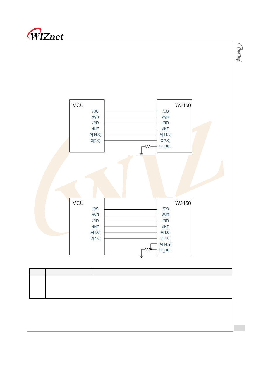
…
…
Ì
Ì
Ô
Ô
Î
Î
Ð
Ð
ø
ø
¨
¨
ø
ø
-
-
∏
∏
ª
ª
ª
ª
¨
¨
¯
¯
ª
ª
Æ
Æ
Ú
Ú
Ô
Ô
Ú
Ú
˜
˜
ÏËÒÎÁ
6. Application Information
For the communication with MCU, W3150 provides Direct Bus I/F and Indirect Bus I/F mode. For the
communication with Ethernet PHY, MII is used.
6.1.Direct Bus I/F Mode.
Direct Bus I/F mode uses 15bit address line and 8bit data line, /CS, /RD, /WR, /INT.
6.2.Indirect Bus I/F Mode.
Indirect Bus I/F mode uses 2bit address line and 8bit data line, /CS, /RD, /WR, /INT.
[14:2], other address lines should process Pull-down.
Indirect bus I/F mode related register is as below.
Value
Symbol
Description
0x00
MR
It performs the selection of Indirect bus I/F mode, Little/Big endian, and
address automatic increase. Refer to 4. Register Description for more
detail.
© Copyright 2005 WIZnet Co., Inc. All rights reserved.

…
…
Ì
Ì
Ô
Ô
Î
Î
Ð
Ð
ø
ø
¨
¨
ø
ø
-
-
∏
∏
ª
ª
ª
ª
¨
¨
¯
¯
ª
ª
Æ
Æ
Ú
Ú
Ô
Ô
Ú
Ú
˜
˜
ÏÁÒÎÁ
0x01
0x02
IDM_AR0
IDM_AR1
Indirect bus I/F mode address Register
MSB/LSB can be decided by LB bit of MODE Register.
1. In case that LB bit is set to 0
0x01
0x02
IDM_AR0 : MSB
IDM_AR1 : LSB
2. In case that LB bit is set to 1
0x01
0x02
IDM_AR0 : LSB
IDM_AR1 : MSB
0x03
IDM_DR
Indirect bus I/F mode data Register
In order to read or write the internal register or internal TX/RX Memory,
1. Write the address to read or write on IDM_AR0,1.
2. Read or Write IDM_DR.
In order to read or write the data on the sequential address, set AI bit of MR(Mode Register). With this, user
performs above 1 only one time. Whenever reading or writing IDM_DR, IDM_AR value increases by 1
automatically. So, the value can be processed on the sequential address just by continuous reading or
writing of IDM_DR.
6.3.MII (Media Independent Interface)
The MII handles the data transfer between the W3150 and the Physical Layer Device.
The MII is composed of TX_CLK, TXE, and TXD[0:3] signals for sending data and RX_CLK, CRS, RXDV,
RXD[0:3], and COL signals for receiving data.
When sending data from the W3150, TXE and TXD[0:3] are output in synchronization with the falling edges
of TX_CLK input from the Physical Layer Device because Physical Layer Devices generally recognize the
rising edges of TX_CLK.
When receiving data, in general, the Physical Layer Devices output CRS, RXDV, RXD[0:3], and COL signals
in synchronization with the falling edges of RX_CLK, so the W3100A recognizes the signals at the rising
edges of RX_CLK.
© Copyright 2005 WIZnet Co., Inc. All rights reserved.

…
…
Ì
Ì
Ô
Ô
Î
Î
Ð
Ð
ø
ø
¨
¨
ø
ø
-
-
∏
∏
ª
ª
ª
ª
¨
¨
¯
¯
ª
ª
Æ
Æ
Ú
Ú
Ô
Ô
Ú
Ú
˜
˜
ÎÒÎÁ
7. Electrical Specification
7.1.Absolute Maximum Ratings
Symbol
Parameter
Rating
Unit
V
DD
DC Supply voltage
-0.3 to 3.6
V
V
IN
DC input voltage
-0.3 to 5.5 (5V tolerant)
V
I
IN
DC input current
15
mA
T
OP
Operating temperature
0 to 80
C
T
STG
Storage temperature
-55 to 125
C
*COMMENT
: Stressing the device beyond the Absolute Maximum Ratings may cause permanent damage.
7.2. DC Characteristics
Symbol
Parameter
Test Condition
Min
Typ
Max
Unit
V
DD
DC Supply voltage
Junction temperature is from -55C
to 125C
3.0
3.6
V
V
IH
High level input voltage
2.0
V
DD
+
0.3
V
V
IL
Low level input voltage
- 0.3
0.3 *
V
DD
V
I
OH
= -100 A
2.9
V
I
OH
= -1 mA
2.4
V
V
OH
High level output voltage
V
DD
= 3.0,
V
I =
V
IH
I
OH
= -2 mA
1.9
V
I
OL
= 100 A
0.2
V
I
OL
= 1 mA
0.4
V
V
OL
Low level output voltage
V
DD
= 3.0,
V
I =
V
IL
I
OL
= 2 mA
0.6
V
I
I
Input Current
V
DD
= 3.6, V
I
= V
DD
or GND
A
15
© Copyright 2005 WIZnet Co., Inc. All rights reserved.

…
…
Ì
Ì
Ô
Ô
Î
Î
Ð
Ð
ø
ø
¨
¨
ø
ø
-
-
∏
∏
ª
ª
ª
ª
¨
¨
¯
¯
ª
ª
Æ
Æ
Ú
Ú
Ô
Ô
Ú
Ú
˜
˜
ÎÔÒÎÁ
7.3. AC Characteristics
7.3.1. Reset Timing
Symbol
Parameter
Min
Max
t
RST
Reset Cycle Time
96 ns
-
t
RLC
/RESET to PLOCK Output
-
125 s
© Copyright 2005 WIZnet Co., Inc. All rights reserved.

…
…
Ì
Ì
Ô
Ô
Î
Î
Ð
Ð
ø
ø
¨
¨
ø
ø
-
-
∏
∏
ª
ª
ª
ª
¨
¨
¯
¯
ª
ª
Æ
Æ
Ú
Ú
Ô
Ô
Ú
Ú
˜
˜
ÎÓÒÎÁ
7.3.2. Register/Memory READ Timing
Symbol
Parameter
Min
Max
t
RC
Read Cycle Time
96 ns
-
t
CVO
/CS to Valid Output
-
96 ns
t
RVO
/RD to Valid Output
-
96 ns
t
CLZ
/CS to Low-Z Output
0 ns
-
t
RLZ
/RD to Low-Z Output
0 ns
-
t
CHZ
/CS to High-Z Output
-
1 ns
t
RHZ
/RD to High-Z Output
-
1 ns
© Copyright 2005 WIZnet Co., Inc. All rights reserved.
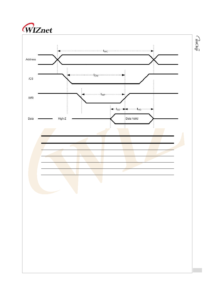
…
…
Ì
Ì
Ô
Ô
Î
Î
Ð
Ð
ø
ø
¨
¨
ø
ø
-
-
∏
∏
ª
ª
ª
ª
¨
¨
¯
¯
ª
ª
Æ
Æ
Ú
Ú
Ô
Ô
Ú
Ú
˜
˜
ÎÌÒÎÁ
7.3.3. Register/Memory WRITE Timing
Symbol
Parameter
Min
Max
t
WC
Write Cycle Time
72 ns
-
t
CW
/CS to Write End
64 ns
-
t
WP
/WR Pulse width
64 ns
-
t
SD
Data Setup to Write End
8 ns
-
t
HD
Data Hold from Write End
8 ns
-
© Copyright 2005 WIZnet Co., Inc. All rights reserved.

…
…
Ì
Ì
Ô
Ô
Î
Î
Ð
Ð
ø
ø
¨
¨
ø
ø
-
-
∏
∏
ª
ª
ª
ª
¨
¨
¯
¯
ª
ª
Æ
Æ
Ú
Ú
Ô
Ô
Ú
Ú
˜
˜
ÎÏÒÎÁ
7.3.4.
MII(Media Independent Interface) Timing
MII Tx TIMING
Symbol
Parameter
Notes
Min
Typ
Max
t
CO
TX_CLK to TXD, TX_EN
10 Mbps
202 ns
-
205 ns
t
DCS
TXD, TX_EN setup time to TX_CLK
10 Mbps
195 ns
-
198 ns
t
CO
TX_CLK to TXD, TX_EN
100 Mbps
22 ns
-
25 ns
t
DCS
TXD, TX_EN setup time to TX_CLK
100 Mbps
15 ns
-
18 ns
© Copyright 2005 WIZnet Co., Inc. All rights reserved.

…
…
Ì
Ì
Ô
Ô
Î
Î
Ð
Ð
ø
ø
¨
¨
ø
ø
-
-
∏
∏
ª
ª
ª
ª
¨
¨
¯
¯
ª
ª
Æ
Æ
Ú
Ú
Ô
Ô
Ú
Ú
˜
˜
ÎÎÒÎÁ
MII Rx TIMING
Symbol
Parameter
Notes
Min
Typ
Max
t
DCS
Valid Data to RX_CLK (setup)
10 Mbps
5 ns
-
-
t
CDH
RX_CLK to Valid Data (hold)
10 Mbps
5 ns
-
-
t
DCS
Valid Data to RX_CLK (setup)
100 Mbps
5 ns
-
-
t
CDH
RX_CLK to Valid Data (hold)
100 Mbps
5 ns
-
-
© Copyright 2005 WIZnet Co., Inc. All rights reserved.

…
…
Ì
Ì
Ô
Ô
Î
Î
Ð
Ð
ø
ø
¨
¨
ø
ø
-
-
∏
∏
ª
ª
ª
ª
¨
¨
¯
¯
ª
ª
Æ
Æ
Ú
Ú
Ô
Ô
Ú
Ú
˜
˜
ÎÍÒÎÁ
8. IR Reflow Temperature Profile (Lead-Free)
Moisture Sensitivity Level at 260oC IR Condition: 2.
Dry Bag Required: Yes
1 year out of bag time at max 30oC/60%RH.
Max. Temperature 260
o
C
Ramp up rate
< 3
o
C/second
Pre-heat temperature at 175∞C(±25∞C)
77-95 seconds
Temperature above 217∞C
96-107 seconds
Time within 5∞C of actual peak temperature
17-25 seconds
Peak temperature range
258-260
o
C
Ramp-down rate
< 6
o
C/second
© Copyright 2005 WIZnet Co., Inc. All rights reserved.

…
…
Ì
Ì
Ô
Ô
Î
Î
Ð
Ð
ø
ø
¨
¨
ø
ø
-
-
∏
∏
ª
ª
ª
ª
¨
¨
¯
¯
ª
ª
Æ
Æ
Ú
Ú
Ô
Ô
Ú
Ú
˜
˜
ÎÈÒÎÁ
9. Package Description
© Copyright 2005 WIZnet Co., Inc. All rights reserved.

…
…
Ì
Ì
Ô
Ô
Î
Î
Ð
Ð
ø
ø
¨
¨
ø
ø
-
-
∏
∏
ª
ª
ª
ª
¨
¨
¯
¯
ª
ª
Æ
Æ
Ú
Ú
Ô
Ô
Ú
Ú
˜
˜
ÎËÒÎÁ
© Copyright 2005 WIZnet Co., Inc. All rights reserved.