
The Western Design Center, Inc.
February 2004 W65C02S Data Sheet
©
The Western Design Center, Inc., 2003. All rights reserved
WDC
W65C02S
Microprocessor
DATA SHEET

The Western Design Center, Inc.
February 2004 W65C02S Data Sheet
The Western Design Center, Inc. W65C02S Data Sheet 2
WDC reserves the right to make changes at any time without notice in order to improve design and supply the best possible
product. Information contained herein is provided gratuitously and without liability, to any user. Reasonable efforts have been
made to verify the accuracy of the information but no guarantee whatsoever is given as to the accuracy or as to its applicability to
particular uses. In every instance, it must be the responsibility of the user to determine the suitability of the products for each
application. WDC products are not authorized for use as critical components in life support devices or systems. Nothing
contained herein shall be construed as a recommendation to use any product in violation of existing patents or other rights of
third parties. The sale of any WDC product is subject to all WDC Terms and Conditions of Sales and Sales Policies, copies of
which are available upon request.
Copyright
©
1981-2004 by The Western Design Center, Inc. All rights reserved, including the right of reproduction, in whole, or
in part, in any form.

The Western Design Center, Inc.
W65C02S Data Sheet
The Western Design Center, Inc. W65C02S Data Sheet
3
TABLE OF CONTENTS
1
INTRODUCTION................................................................................................................................................................................5
1.1
F
EATURES OF THE
W65C02S..................................................................................................................................................... 5
2
FUNCTIONAL DESCRIPTION......................................................................................................................................................6
2.1
I
NSTRUCTION
R
EGISTER
(IR)
AND
D
ECODE
........................................................................................................................... 6
2.2
T
IMING
C
ONTROL
U
NIT
(TCU) ................................................................................................................................................. 6
2.3
A
RITHMETIC AND
L
OGIC
U
NIT
(ALU) ..................................................................................................................................... 6
2.4
A
CCUMULATOR
R
EGISTER
(A)................................................................................................................................................... 6
2.5
I
NDEX
R
EGISTERS
(X
AND
Y)...................................................................................................................................................... 6
2.6
P
ROCESSOR
S
TATUS
R
EGISTER
(P) ........................................................................................................................................... 6
2.7
P
ROGRAM
C
OUNTER
R
EGISTER
(PC)....................................................................................................................................... 6
2.8
S
TACK
P
OINTER
R
EGISTER
(S) .................................................................................................................................................. 7
3
PIN FUNCTION DESCRIP TION ...................................................................................................................................................9
3.1
A
DDRESS
B
US
(A0-A15)............................................................................................................................................................... 9
3.2
B
US
E
NABLE
(BE).......................................................................................................................................................................... 9
3.3
D
ATA
B
US
(D0-D7)........................................................................................................................................................................ 9
3.4
I
NTERRUPT
R
EQUEST
(IRQB).................................................................................................................................................... 9
3.5
M
EMORY
L
OCK
(MLB) ............................................................................................................................................................... 9
3.6
N
O N
-M
ASKABLE
I
NTERRUPT
(NMIB)...................................................................................................................................... 9
3.7
N
O
C
ONNECT
(NC) ..................................................................................................................................................................... 10
3.8
P
HASE
2
I
N
(PHI2),
P
HASE
2
O
UT
(PHI2O)
AND
P
HASE
1
O
UT
(PHI1O) ...................................................................... 10
3.9
R
EAD
/W
RITE
(RWB) ................................................................................................................................................................. 10
3.10
R
EADY
(RDY) .............................................................................................................................................................................. 10
3.11
R
ESET
(RESB) ............................................................................................................................................................................. 11
3.12
S
ET
O
VERFLOW
(SOB).............................................................................................................................................................. 11
3.13
SYNC
HRONIZE WITH
O
P
C
ODE FETCH
(SYNC)................................................................................................................... 11
3.14
P
OWER
(VDD)
AND
G
ROUND
(VSS)........................................................................................................................................ 11
3.15
V
ECTOR
P
ULL
(VPB) ................................................................................................................................................................. 11
4
ADDRESSING MODES ...................................................................................................................................................................16
4.1
A
BSOLUTE A
.................................................................................................................................................................................. 16
4.2
A
BSOLUTE
I
NDEXED
I
NDIRECT
(
A
,
X
) ...................................................................................................................................... 16
4.3
A
BSOLUTE
I
NDEXED WITH
X
A
,
X
............................................................................................................................................. 16
4.4
A
BSOLUTE
I
NDEXED WITH
Y
A
,
Y
............................................................................................................................................ 17
4.5
A
BSOLUTE
I
NDIRECT
(
A
)............................................................................................................................................................ 17
4.6
A
CCUMULATOR
A ....................................................................................................................................................................... 17
4.7
I
MMEDIATE
A
DDRESSING
#....................................................................................................................................................... 17
4.8
I
MPLIED I
....................................................................................................................................................................................... 17
4.9
P
ROGRAM
C
OUNTER
R
ELATIVE R
........................................................................................................................................... 18
4.10
S
TACK S
......................................................................................................................................................................................... 18
4.11
Z
ERO
P
AGE ZP
.............................................................................................................................................................................. 18
4.12
Z
ERO
P
AGE
I
NDEXED
I
NDIRECT
(
ZP
,
X
) .................................................................................................................................. 18
4.13
Z
ERO
P
AGE
I
NDEXED WITH
X
ZP
,
X
......................................................................................................................................... 19
4.14
Z
ERO
P
AGE
I
NDEXED WITH
Y
ZP
,
Y
........................................................................................................................................ 19
4.15
Z
ERO
P
AGE
I
NDIRECT
(
ZP
)........................................................................................................................................................ 19
4.16
Z
ERO
P
AGE
I
NDIRECT
I
NDEXED WITH
Y
(
ZP
),
Y
.................................................................................................................. 19
5
OPERATION TABLES ....................................................................................................................................................................21
6
DC, AC AND TIMING CHARACTERISTICS .........................................................................................................................23

The Western Design Center, Inc.
W65C02S Data Sheet
The Western Design Center, Inc. W65C02S Data Sheet
4
6.1
DC
C
HARACTERISTICS
TA
=
-40
∞
C
TO
+85
∞
C
(PLCC,
QFP)
TA=
0
∞
C
TO
70
∞
C
(DIP) .......................................... 24
6.2
AC
C
HARACTERISTICS
TA
=
-40
∞
C
TO
+85
∞
C
(PLCC,
QFP)
TA=
0
∞
C
TO
70
∞
C
(DIP) .......................................... 25
7
CAVEATS ............................................................................................................................................................................................36
8
W65C02DB DEVELOPER BOARD AND .................................................................................................................................37
IN-CIRCUIT EMULATOR (ICE)..........................................................................................................................................................37
8.1
F
EATURES
:.................................................................................................................................................................................... 38
8.2
M
EMORY MAP
:............................................................................................................................................................................. 38
8.3
C
ROSS
-D
EBUGGING
M
ONITOR
P
ROGRAM
............................................................................................................................. 38
8.4
BUILDING................................................................................................................................................................................... 38
9
HARD CORE MODEL .....................................................................................................................................................................39
9.1
F
EATURES OF THE
W65C02S
H
ARD
C
ORE
M
ODEL
................................................................................................................. 39
10
SOFT CORE RTL MODEL ........................................................................................................................................................39
10.1
W65C02
S
YNTHESIZABLE
RTL-C
ODE IN
V
ERILOG
HDL................................................................................................. 39
TABLE OF TABLES
TABLE 3 -1 VECTOR LOCATIONS....................................................................................................................................................12
TABLE 3 -2 PIN FUNCTION TABLE..................................................................................................................................................12
TABLE 4 -1 ADDRESSING MODE TABLE......................................................................................................................................20
TABLE 5 -1 INSTRUCTION SET TABLE .........................................................................................................................................21
TABLE 5 -2 W65C02S OPCODE MATRIX ........................................................................................................................................22
TABLE 6 -1 ABSOLUTE MAXIMUM RATINGS ............................................................................................................................23
TABLE 6 -2 DC CHARACTERISTICS................................................................................................................................................24
TABLE 6 -3 AC CHARACTERISTICS ..............................................................................................................................................25
TABLE 6 -4 OPERATION, OPERATION CODES AND STATUS REGISTER.....................................................................28
TABLE 6 -5 INSTRUCTION TIMING CHART ...............................................................................................................................32
TABLE 7 -1 MICROPROCESSOR OPERATIONAL ENHANCEMENTS ..............................................................................36
TABLE OF FIGURES
FIGURE 2-1 W65C02S INTERNAL ARCHITECTURE SIMPLIFIED BLOCK DIAGRAM.............................................7
FIGURE 2-2 W65C02S MICROPROCESSOR PROGRAMMING MODEL ............................................................................8
FIGURE 3-1 W65C02S 40 PIN PDIP PINOUT .................................................................................................................................13
FIGURE 3-2 W65C02S 44 PIN PLCC PINOUT ...............................................................................................................................14
FIGURE 3-3 W65C02S 44 PIN QFP PINOUT ..................................................................................................................................15
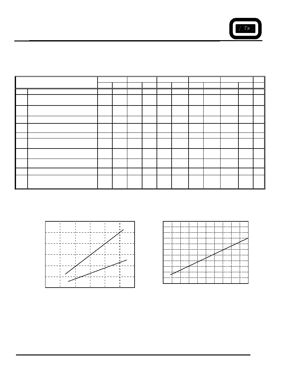
FIGURE 6-1 IDD VS VDD .....................................................................................................................................................................24
FIGURE 6-2 F MAX VS VDD...............................................................................................................................................................24
FIGURE 6-3 GENERAL TIMING DIAGRAM ................................................................................................................................26

The Western Design Center, Inc.
W65C02S Data Sheet
The Western Design Center, Inc. W65C02S Data Sheet
5
1
INTRODUCTION
The W65C02S is a low power cost sensitive 8-bit microprocessor. The W65C02S is a fully static core and the PHI2 clock
can be stopped when it is in the high (logic 1) or low (logic 0) state. The variable length instruction set and manually
optimized core size makes the W65C02S an excellent choice for low power System-on-Chip (SoC) designs. The Verilog
RTL model is available for ASIC design flows. WDC, a Fabless Semiconductor Company, provides packaged chips for
evaluation or volume production. To aid in system development, WDC provides a Development System that includes a
W65C02DB Developer Board, an In-Circuit Emulator (ICE) and the W65cSDS Software Development System, see
www.westerndesigncenter.com for more information.
1.1
Features of the W65C02S
∑
8-bit data bus
∑
16-bit address bus provides access to 65,536 bytes of memory space
∑
8-bit ALU, Accumulator, Stack Pointer, Index Registers, Processor Status Register
∑
16-bit Program Counter
∑
69 instructions
∑
16 addressing modes
∑
212 Operation Codes (OpCodes)
∑
Vector Pull (VPB) output indicates when interrupt vectors are being addressed
∑
WAit-for-Interrupt (WAI) and SToP (STP) instructions reduce power consumption, decrease interrupt latency and
provide synchronization with external events
∑
Variable length instruction set provides for lower power and smaller code optimization over fixed length instruction
set processors
∑
Fully static circuitry
∑
Wide operating voltage range, 1.8+/- 5%, 2.5+/- 5%, 3.0+/- 5%, 3.3+/ - 10%, 5.0+/- 5% specified
∑
Low Power consumption, 150uA@1MHz

The Western Design Center, Inc.
W65C02S Data Sheet
The Western Design Center, Inc. W65C02S Data Sheet
6
2
FUNCTIONAL DESCRIPTION
The internal organization of the W65C02S is divided into two parts: 1) Register Section and 2) Control Section.
Instructions obtained from program memory are executed by implementing a series of data transfers within the
Register Section. Signals that cause data transfers are generated within the Control Section.
2.1
Instruction Register (IR) and Decode
The Operation Code (OpCode) portion of the instruction is loaded into the Instruction Register from the Data Bus
and is latched during the OpCode fetch cycle. The OpCode is then decoded, along with timing and interrupt signals,
to generate various control signals for program execution.
2.2
Timing Control Unit (TCU)
The Timing Control Unit (TCU) provides timing for each instruction cycle that is executed. The TCU is set to zero for each
instruction fetch, and is advanced at the beginning of each cycle for as many cycles as is required to complete the instruction.
Data transfers between registers depend upon decoding the contents of both the IR and the TCU.
2.3
Arithmetic and Logic Unit (ALU)
All arithmetic and logic operations take place within the ALU. In addition to data operations, the ALU also
calculates the effective address for relative and indexed addressing modes. The result of a data operation is stored in
either memory or an internal register. Carry, Negative, Overflow and Zero flags are updated
following the ALU data
operation.
2.4
Accumulator Register (A)
The Accumulator Register (A) is an 8-bit general purpose register which holds one of the operands and the result of
arithmetic and logical operations. Reconfigured versions of this processor family could have additional
accumulators.
2.5
Index Registers (X and Y)
There are two 8-bit Index Registers (X and Y) which may be used as general purpose registers or to provide an index
value for calculation of the effective address. When executing an instruction with indexed addressing, the
microprocessor fetches the OpCode and the base address, and then modifies the address by adding the Index
Register contents to the address prior to performing the desired operation.
2.6
Processor Status Register (P)
The 8-bit Processor Status Register (P) contains status flags and mode select bits. The Carry (C), Negative (N),
Overflow (V) and Zero (Z) status flags serve to report the status of ALU operations. These status flags are tested
with Conditional Branch instructions. The Decimal (D) and IRQB disable (I) are used as mode select flags. These
flags are set by the program to change microprocessor operations. Bit 5 is available for a user status or mode bit.
2.7
Program Counter Register (PC)
The Western Design Center, Inc.
W65C02S Data Sheet
The Western Design Center, Inc. W65C02S Data Sheet
7
The 16-bit Program Counter Register (PC) provides the addresses which are used to step the microprocessor through
sequential program instructions. This register is incremented each time an instruction or operand is fetched from
program memory.
2.8
Stack Pointer Register (S)
The Stack Pointer Register (S) is an 8-bit register which is used to indicate the next available location in the stack
memory area. It serves as the effective address in stack addressing modes as well as subroutine and interrupt
processing.
IRQB
NMIB
RESB
A0-A15
PHI2
D0-D7
Figure 2-1 W65C02S Internal Architecture Simplified Block Diagram
INTERNAL ADDRESS BUS (16 BITS)
ADDRESS BUFFER
INDEX X
(8 BITS)
INDEX Y
(8 BITS)
STACK POINTER
(S) (8 BITS)
ALU
(8 BITS)
ACCUMULATOR
(A) ( 8BITS)
PROG. COUNTER
(PC) (16 BITS)
PROCESSOR
STATUS
(P) 8 BITS
DATA
LATCH
BE
INSTRUCTION REGISTER
(8 BITS)
INSTRUCTION
DECODE
INTERRUPT
LOGIC
TIMING
CONTROL
BE
INTERNAL DATA BUS (8 BITS)
DATA BUS BUFFER
SYSTEM
CONTROL
BE
RWB
RDY
VPB
SYNC
The Western Design Center, Inc.
W65C02S Data Sheet
The Western Design Center, Inc. W65C02S Data Sheet
8
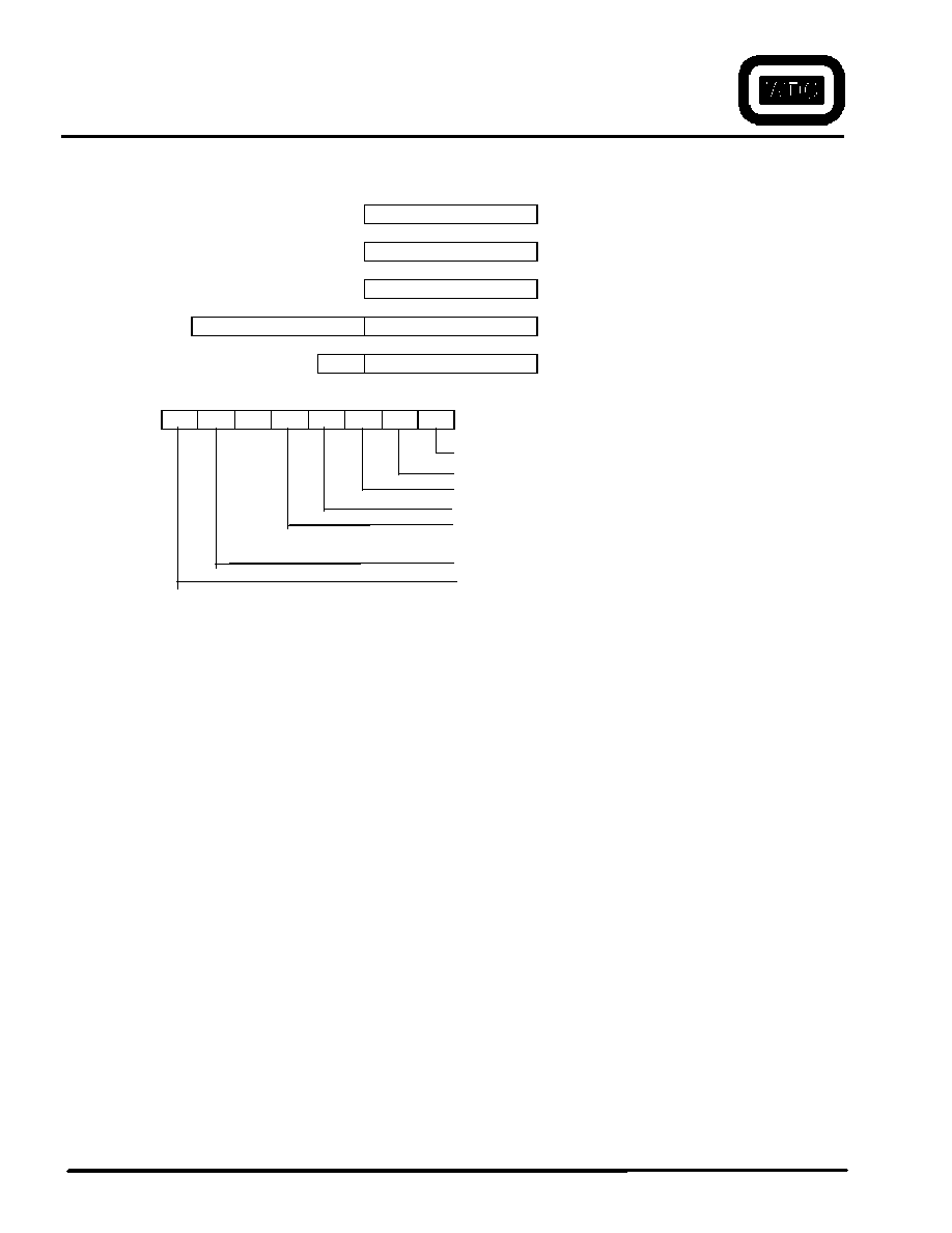
A
Accumulator A
Y
Index Register Y
X
Index Register X
PCH
PCL
Program Counter PC
1
S
Stack Pointer S
N
V
1
B
D
I
Z
C
Processor Status Register "P"
Carry 1 = true
Zero 1 = result
IRQB disable 1 = disable
Decimal mode 1= true
BRK command 1 = BRK, 0 = IRQB
Overflow 1 = true
Negative 1 = neg.
Figure 2-2 W65C02S Microprocessor Programming Model
15
0
0
0
0
7
8
7
7
7
7
0

The Western Design Center, Inc.
W65C02S Data Sheet
The Western Design Center, Inc. W65C02S Data Sheet
9
3
PIN FUNCTION DESCRIPTION
3.1
Address Bus (A0-A15)
The sixteen bit Address Bus formed by
A0-A15, address
memory and I/O registers that exchange data on the Data
Bus. The address lines can be set to the high impedance state by the Bus Enable (BE) signal.
3.2
Bus Enable (BE)
The Bus Enable
(BE)
input signal provides external control of the Address, Data and the RWB buffers. When Bus
Enable is high, the Address, Data and RWB buffers are active. When BE is low, these buffers are set to the high
impedance status. Bus Enable is an asynchronous signal.
3.3
Data Bus (D0-D7)
The eight Data Bus lines
D0-D7 are used to
provide instructions, data and addresses to the microprocessor and
exchange data with memory and I/O registers. These lines may be set to the high impedance state by the Bus Enable
(BE) signal.
3.4
Interrupt Request (IRQB)
The Interrupt Request (IRQB) input signal is used to request that an interrupt sequence be initiated. The program
counter (PC) and Processor Status Register (P) are pushed onto the stack and the IRQB disable (I) flag is set to a "1"
disabling further interrupts before jumping to the interrupt handler. These values are used to return the processor to
its original state prior to the IRQB interrupt. The IRQB low level should be held until the interrupt handler clears
the interrupt request source. When Return from Interrupt (RTI) is executed the (I) flag is restored and a new
interrupt can be handled. If the (I) flag is cleared in an interrupt handler, nested interrupts can occur. The Wait-for-
Interrupt (WAI) instruction may be used to reduce power and synchronize with, as an example timer interrupt
requests.
3.5
Memory Lock (MLB)
The Memory Lock (MLB) output may be used to ensure the integrity of Read-Modify-Write instructions in a
multiprocessor system. Memory Lock indicates the need to defer arbitration of the bus cycle when MLB is low.
Memory Lock is low during the last three cycles of ASL, DEC, INC, LSR, ROL, ROR, TRB, and TSB memory
referencing instructions.
3.6
Non-Maskable Interrupt (NMIB)
A negative transition on the Non-Maskable Interrupt (NMIB) input initiates an interrupt sequence after the current
instruction is completed. Since NMIB is an edge-sensitive input, an interrupt will occur if there is a negative
transition while servicing a previous interrupt. Also, after the edge interrupt occurs no further interrupts will occur if
NMIB remains low. The NMIB signal going low causes the Program Counter (PC) and Processor Status Register
information to be pushed onto the stack before jumping to the interrupt handler. These values are used to return the
processor to it's original state prior to the NMIB interrupt.

The Western Design Center, Inc.
W65C02S Data Sheet
The Western Design Center, Inc. W65C02S Data Sheet
10
3.7
No Connect (NC)
The No Connect (NC) pins are not connected internally and should not be connected externally.
3.8
Phase 2 In (PHI2), Phase 2 Out (PHI2O) and Phase 1 Out (PHI1O)
Phase 2 In (PHI2) is the system clock input to the microprocessor internal clock. During the low power Standby
Mode, PHI2 can be held in either high or low state to preserve the contents of internal registers since the
microprocessor is a fully static design. The Phase 2 Out (PHI2O) signal is generated from PHI2. Phase 1 Out
(PHI1O) is the inverted PHI2 signal. An external oscillator is recommended for driving PHI2 and used for the main
system clock. All production test timing is based on PHI2. PHI2O and PHI1O were used in older systems for
system timing and internal oscillators when an external crystal was used.
3.9
Read/Write (RWB)
The Read/Write (RWB) output signal is used to control data transfer. When in the high state, the microprocessor is
reading data from memory or I/O. When in the low state, the Data Bus contains valid data to be written from the
microprocessor and stored at the addressed memory or I/O location. The RWB signal is set to the high impedance
state when Bus Enable (BE) is low.
3.10
Ready (RDY)
A low input logic level on the Ready (RDY) will halt the microprocessor in its current state. Returning RDY to the
high state allows the microprocessor to continue operation following the next PHI2 negative transition. This bi-
directional signal allows the user to single -cycle the microprocessor on all cycles including write cycles. A negative
transition to the low state prior to the falling edge of PHI2 will halt the microprocessor with the output address lines
reflecting the current address being fetched. This assumes the processor setup time is met. This condition will
remain through a subsequent PHI2 in which the ready signal is low. This feature allows microprocessor interfacing
with low-speed memory as well as direct memory access (DMA). The WAI instruction pulls RDY low signaling the
WAit-for-Interrupt condition, thus RDY is a bi-directional pin. On the W65C02 hard core there is a WAIT output
signal that can be used in ASIC's thus removing the bi-directional signal and RDY becomes only the input. In such
a situation the WAI instruction will pull WAIT low and must be used external of the core to pull RDY low or the
processor will continue as if the WAI never happened. The microprocessor will be released when RDY is high and
a falling edge of PHI2 occurs. This again assumes the processor control setup time is met. The RDY pin has an
active pull-up, when outputting a low level, the pull-up is disabled. The RDY pin can still be wire ORed.
The Western Design Center, Inc.
W65C02S Data Sheet
The Western Design Center, Inc. W65C02S Data Sheet
11
3.11
Reset (RESB)
The Reset (RESB) input is used to initialize the microprocessor and start program execution. The RESB signal must
be held low for at least two clock cycles after VDD reaches operating voltage. Ready (RDY) has no effect while
RESB is being held low. All Registers are initialized by software except the Decimal and Interrupt disable mode
select bits of the Processor Status Register (P) are initialized by hardware. When a positive edge is detected, there
will be a reset sequence lasting seven clock cycles. The program counter is loaded with the reset vector from
locations FFFC (low byte) and FFFD (high byte). This is the start location for program control. RESB should be
held high after reset for normal operation.
Processor Status Register (P)
7
6
5
4
3
2
1
0
*
*
1
1
0
1
*
*
N
V
B
D
I
Z
C
*=software initialized
3.12
Set Overflow (SOB)
A negative transition on the
Set Overflow (SOB)
pin sets the overflow bit (V) in the status code register. The signal is
sampled on the rising edge of PHI2. SOB was originally intended for fast input recognition because it can be tested
with a branch instruction; however, it is not recommended in new system design and was seldom used in the past.
3.13
SYNChronize with OpCode fetch (SYNC)
The OpCode fetch cycle of the microprocessor instruction is indicated with SYNC high. The SYNC output is
provided to identify those cycles during which the microprocessor is fetching an OpCode. The SYNC line goes high
during the clock cycle of an OpCode fetch and stays high for the entire cycle. If the RDY line is pulled low during
the clock cycle in which SYNC went high, the processor will stop in its current state and will remain in the state
until the RDY line goes high. In this manner, the SYNC signal can be used to control RDY to cause single
instruction execution.
3.14
Power (VDD) and Ground (VSS)
VDD is the positive power supply voltage and VSS is system logic ground.
3.15
Vector Pull (VPB)
The Vector Pull (VPB) output indicates that a vector location is being addressed during an interrupt sequence. VPB
is low during the last interrupt sequence cycles, during which time the processor reads the interrupt vector. The
VPB signal may be used to select and prioritize interrupts from several sources by modifying the vector addresses.
The Western Design Center, Inc.
W65C02S Data Sheet
The Western Design Center, Inc. W65C02S Data Sheet
12
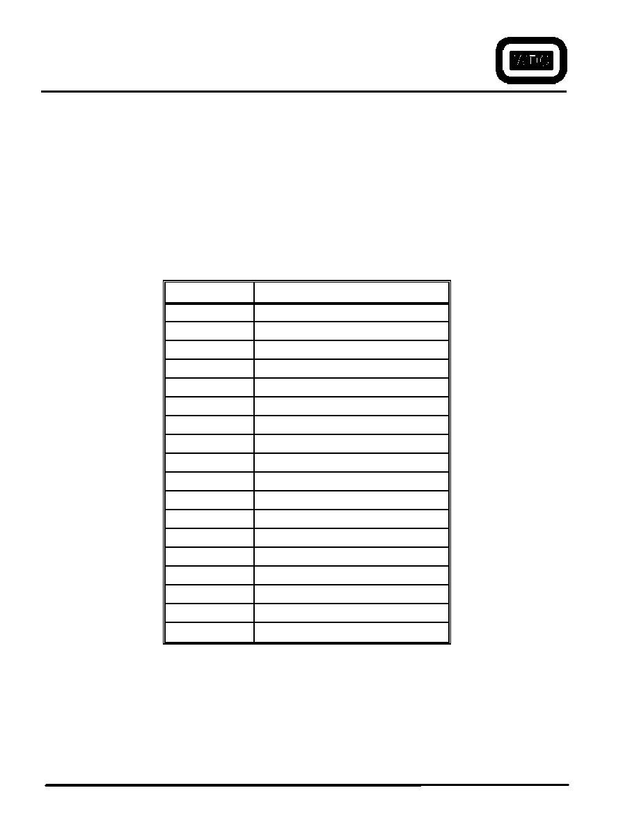
Table 3-1
Vector Locations
FFFE, F
BRK/IRQB
Software/Hardware
FFFC, D
RESB
Hardware
FFFA, B
NMIB
Hardware
Table 3-2 Pin Function Table
Pin
Description
A0-A15
Address Bus
BE
Bus Enable
D0-D7
Data Bus
IRQB
Interrupt Request
MLB
Memory Lock
NC
No Connection
NMIB
Non-Maskable Interrupt
PHI1O
Phase 1 Out Clock
PHI2
Phase 2 In Clock
PHI2O
Phase 2 Out Clock
RDY
Ready
RESB
Reset
RWB
Read/Write
SOB
Set Overflow
SYNC
Synchronize
VDD
Positive Power Supply
VPB
Vector Pull
VSS
Internal Logic Ground
The Western Design Center, Inc.
W65C02S Data Sheet
The Western Design Center, Inc. W65C02S Data Sheet
13
VPB
RDY
PHI1O
IRQB
MLB
NMIB
SYNC
VDD
A0
A1
A2
A3
A4
A5
A6
A7
A8
A9
A10
A11
1
2
3
4
5
6
7
8
9
10
11
12
13
14
15
16
17
18
19
20
40
39
38
37
36
35
34
33
32
31
30
29
28
27
26
25
24
23
22
21
RESB
PHI2C
SOB
PHI2
BE
NC
RWB
D0
D1
D2
D3
D4
D5
D6
D7
A15
A14
A13
A12
VSS
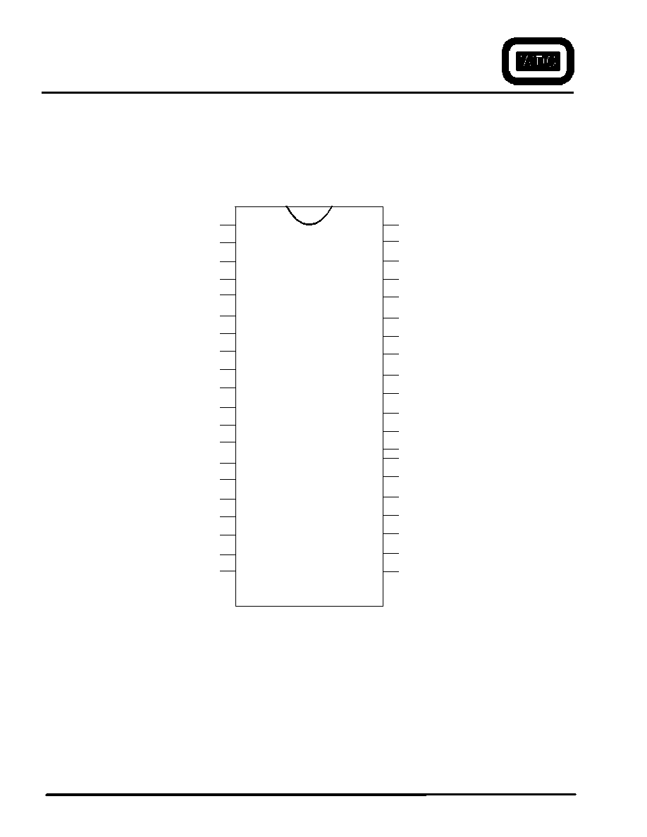
Figure 3-1 W65C02S 40 Pin PDIP Pinout
The Western Design Center, Inc.
W65C02S Data Sheet
The Western Design Center, Inc. W65C02S Data Sheet
14
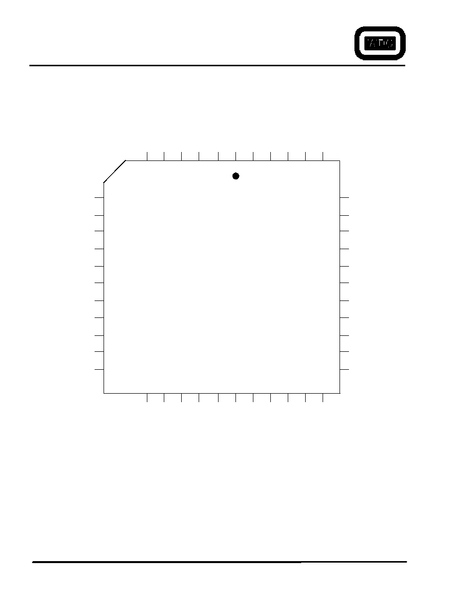
Figure 3-2 W65C02S 44 Pin PLCC Pinout
NC
RWB
VDD
D0
D1
D2
D3
D4
D5
D6
D7
NMIB
SYNC
VDD
A0
A1
NC
A2
A3
A4
A5
A6
7
8
9
10
11
12
13
14
15
16
17
39
38
37
36
35
34
33
32
31
30
29
MLB
IRQB
PHI1O
RDY
VPB
VSS
RESB
PHI2O
SOB
PHI2
BE
A7
A8
A9
A10
A11
VSS
VSS
A12
A13
A14
A15
W65C02
18 19 20 21 22 23 24 25 26 27 28
6 5 4 3 2 1 44 43 42 41 40
The Western Design Center, Inc.
W65C02S Data Sheet
The Western Design Center, Inc. W65C02S Data Sheet
15
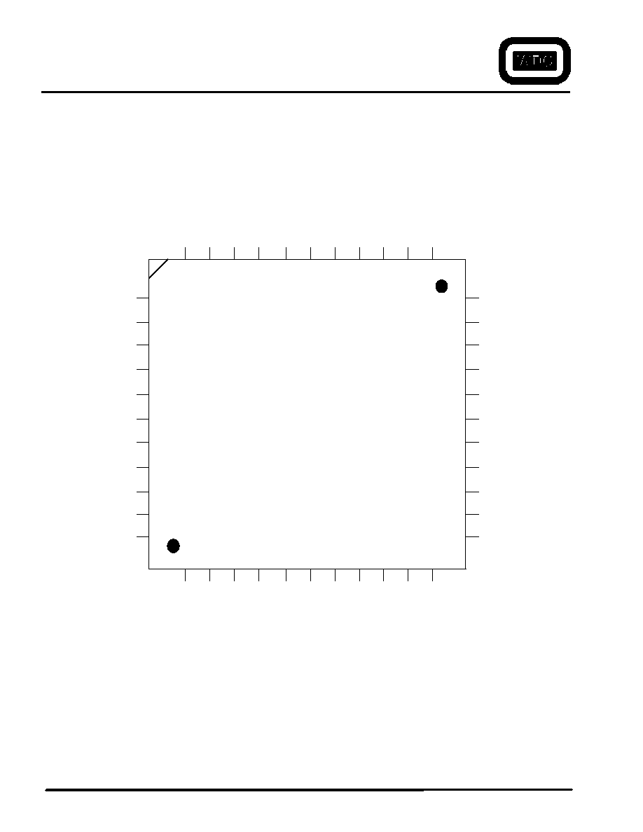
Figure 3-3 W65C02S 44 Pin QFP Pinout
NMIB
SYNC
VDD
A0
A1
NC
A2
A3
A4
A5
A6
1
2
3
4
5
6
7
8
9
10
11
MLB
IRQB
PHI1O
RDY
VPB
VSS
RESB
PHI2O
SOB
PHI2
BE
44 43 42 41 40 39 38 37 36 35 34
NC
RWB
VDD
D0
D1
D2
D3
D4
D5
D6
D7
33
32
31
30
29
28
27
26
25
24
23
12 13 14 15 16 17 18 19 20 21 22
A7
A8
A9
A10
A11
VSS
VSS
A12
A13
A14
A15
The Western Design Center, Inc.
W65C02S Data Sheet
The Western Design Center, Inc. W65C02S Data Sheet
16
4
ADDRESSING MODES
The W65C02S is capable of directly addressing 65,536 bytes of memory. The Program Address and Data Address space is
contiguous throughout the 65,536 byte address space. Words, arrays, records, or any data structures may span the 65,536
byte address space. The following addressing mode descriptions provide additional detail as to how effective addresses are
calculated. Sixteen addressing modes are available for the W65C02S. This address space has special significance within
certain addressing modes.
4.1
Absolute a
With Absolute addressing the second and third bytes of the instruction form the 16-bit address.
Byte:
2
1
0
Instruction:
ADH
ADL
OpCode
Operand Address:
ADH
ADL
4.2
Absolute Indexed Indirect (a,x)
With the Absolute Indexed Indirect addressing mode, the X Index Register is added to the second and third byes of the
instruction to form an address to a pointer. This address mode is only used with the JMP instruction and the program
Counter is loaded with the first and second bytes at this pointer.
Byte:
2
1
0
Instruction:
ADH
ADL
OpCode
Indirect Base address:
ADH
ADL
+
X
Indirect address:
effective address
New PC value:
indirect address
4.3
Absolute Indexed with X a,x
With the Absolute Indexed with X addressing mode, the X Index Register is added to the second and third bytes of the
instruction to form the 16-bits of the effective address.
Byte:
2
1
0
Instruction:
ADH
ADL
OpCode
ADH
ADL
+
X
Operand address:
effective address
The Western Design Center, Inc.
W65C02S Data Sheet
The Western Design Center, Inc. W65C02S Data Sheet
17
4.4
Absolute Indexed with Y a, y
With the Absolute Indexed with Y addressing mode, the Y Index Register is added to the second and third bytes of the
instruction to form the 16-bit effective address.
Byte:
2
1
0
Instruction:
ADH
ADL
OpCode
ADH
ADL
+
Y
Operand address:
effective address
4.5
Absolute Indirect (a)
With the Absolute Indirect addressing mode, the second and third bytes of the instruction form an address to a pointer. This
address mode is only used with the JMP instruction and the Program Counter is loaded with the first and second bytes at this
pointer.
Byte:
2
1
0
Instruction:
ADH
ADL
OpCode
Indirect address:
ADH
ADL
New PC value:
indirect address
4.6
Accumulator A
With Accumulator addressing the operand is implied as the Accumulator and therefore only a single byte forms the
instruction..
Byte:
2
1
0
Instruction:
OpCode
Operand:
accumulator
4.7
Immediate Addressing #
With Immediate Addressing the operand is the second byte of the instruction.
Byte:
2
1
0
Instruction:
Operand
OpCode
Operand:
Operand
4.8
Implied i
Implied addressing uses a single byte instruction. The operand is implicitly defined by the instruction.
Byte:
2
1
0
Instruction:
OpCode
Operand address:
implied

The Western Design Center, Inc.
W65C02S Data Sheet
The Western Design Center, Inc. W65C02S Data Sheet
18
4.9
Program Counter Relative r
The Program Counter relative addressing mode, sometimes referred to as Relative Addressing, is used with the Branch
instructions. If the condition being tested is met, the second byte of the instruction is added to the Program Counter and
program control is transferred to this new memory location.
Byte:
2
1
0
Instruction:
offset
OpCode
PCH
PCL
+
offset
New PC value
effective address
4.10
Stack s
The Stack may use memory from 0100 to 01FF and the effective address of the Stack address mode will always be within
this range. Stack addressing refers to all instructions that push or pull data from the stack, such as Push, Pull, Jump to
Subroutine, Return from Subroutine, Interrupts and Return from Interrupt.
Byte:
2
1
0
Instruction:
OpCode
Operand address:
1
S
4.11
Zero Page zp
With Zero Page (zp) addressing the second byte of the instruction is the address of the operand in page zero.
Byte:
2
1
0
Instruction:
zp
OpCode
Operand address:
0
zp
4.12
Zero Page Indexed Indirect (zp,x)
The Zero Page Indexed Indirect addressing mode is often referred to as Indirect,X. The second byte of the instruction is the
zero page address to which the X Index Register is added and the result points to the low byte of the indirect address.
Byte:
2
1
0
Instruction:
zp
OpCode
Base Address:
zp
+
X
Indirect Address:
0
address
Operand address:
indirect address

The Western Design Center, Inc.
W65C02S Data Sheet
The Western Design Center, Inc. W65C02S Data Sheet
19
4.13
Zero Page Indexed with X zp,x
With Zero Page Indexed with X addressing mode, the X Index Register is added to the second byte of instruction to form the
effective address.
Byte:
2
1
0
Instruction:
zp
OpCode
Base Address:
zp
+
X
Operand Address:
0
effective address
4.14
Zero Page Indexed with Y zp, y
With Zero Page Indexed with Y addressing, the second byte of the instruction is the zero page address to which the Y Index
Register is added to form the page zero effective address.
Byte:
2
1
0
Instruction:
zp
OpCode
Base Address:
zp
+
Y
Operand Address:
0
effective address
4.15
Zero Page Indirect (zp)
With Zero Page Indirect addressing mode, the second byte of the instruction is a zero page indirect address that points to the
low byte of a two byte effective address.
Byte:
2
1
0
Instruction:
zp
OpCode
Indirect Address:
0
zp
Operand Address:
indirect address
4.16
Zero Page Indirect Indexed with Y (zp), y
The Zero Page Indirect Indexed with Y addressing mode is often referred to as Indirect Y. The second byte of the instruction
points to the low byte of a two byte (16-bit) base address in page zero. Y Index Register is added to the base address to form
the effective address.
Byte:
2
1
0
Instruction:
zp
OpCode
Indirect Base Address:
0
zp
indirect base address
+
Y
Operand Address:
effective address
The Western Design Center, Inc.
W65C02S Data Sheet
The Western Design Center, Inc. W65C02S Data Sheet
20
Table 4-1 Addressing Mode Table
Address Mode
Instruction Times in Memory
Cycle
Memory Utilization in Number of
Program Sequence Bytes
Original
NMOS 6502
W65C02S
Original
NMOS 6502
W65C02S
1.
Absolute a
4 (3)
4 (3)
3
3
2.
Absolute Indexed Indirect (a,x)
5
5
3
3
3.
Absolute Indexed with X a,x
4 (1,3)
4 (1,3)
3
3
4.
Absolute Indexed with Y a,y
4 (1)
4 (1)
3
3
5.
Absolute Indirect (a)
4 (3)
4 (3)
3
3
6.
Accumulator A
2
2
1
1
7.
Immediate #
2
2
2
2
8.
Implied i
2
2
1
1
9.
Program Counter Relative r
2 (2)
2 (2)
2
2
10.
Stack s
3-7
3-7
1-3
1-4
11.
Zero Page zp
3 (3)
3 (3)
2
2
12.
Zero Page Indexed Indirect (zp,x)
6
6
2
2
13.
Zero Page Indexed with X zp,x
4 (3)
4 (3)
2
2
14.
Zero Page Indexed with Y zp,y
4
4
2
2
15.
Zero Page Indirect (zp)
-
5
-
2
16.
Zero Page Indirect Indexed with Y (zp),y
5
5
2
2
Notes: (indicated in parenthesis)
1.
Page boundary, add 1 cycle if page boundary is crossed when forming address
2.
Branch taken, add 1 cycle if branch is taken
3.
Read-Modify-Write, add 2 cycles
The Western Design Center, Inc.
W65C02S Data Sheet
The Western Design Center, Inc. W65C02S Data Sheet
21
5
OPERATION TABLES
Table 5-1 Instruction Set Table
1.
ADC
ADd memory to accumulator with Carry
2.
AND
"AND" memory with accumulator
3.
ASL
Arithmetic Shift one bit Left, memory or
accumulator
4.
∑
BBR
Branch on Bit Reset
5.
∑
BBS
Branch of Bit Set
6.
BCC
Branch on Carry Clear (Pc=0)
7.
BCS
Branch on Carry Set (Pc=1)
8.
BEQ
Branch if EQual (Pz=1)
9.
BIT
BIt Test
10.
BMI
Branch if result MInus (Pn=1)
11.
BNE
Branch if Not Equal (Pz=0)
12.
BPL
Branch if result PLus (Pn=0)
13.
∑
BRA
BRanch Always
14.
BRK
BReaK instruction
15.
BVC
Branch on oVerflow Clear (Pv=0)
16.
BVS
Branch on oVerflow Set (Pv=1)
17.
CLC
CLear Cary flag
18.
CLD
CLear Decimal mode
19.
CLI
CLear Interrupt disable bit
20.
CLV
CLear oVerflow flag
21.
CMP
CoMPare memory and accumulator
22.
CPX
ComPare memory and X register
23.
CPY
ComPare memory and Y register
24.
DEC
DECrement memory or accumulate by one
25.
DEX
DEcrement X by one
26.
DEY
DEcrement Y by one
27.
EOR
"Exclusive OR" memory with accumulate
28.
INC
INCrement memory or accumulate by one
29.
INX
INcrement X register by one
30.
INY
INcrement Y register by one
31.
JMP
JuMP to new location
32.
JSR
Jump to new location Saving Return (Jump to
SubRoutine)
33.
LDA
LoaD Accumulator with memory
34.
LDX
LoaD the X register with memory
35.
LDY
LoaD the Y register with memory
36.
LSR
Logical Shift one bit Right memory or accumulator
37.
NOP
No OPeration
38.
ORA
"OR" memory with Accumulator
39.
PHA
PusH Accumulator on stack
40.
PHP
PusH Processor status on stack
41.
PHX
PusH X register on stack
42.
PHY
PusH Y register on stack
43.
PLA
PuLl Accumulator from stack
44.
PLP
PuLl Processor status from stack
45.
∑
PLX
PuLl X register from stack
46.
∑
PLY
PuLl Y register from stack
47.
∑
RMB
Reset Memory Bit
48.
ROL
ROtate one bit Left memory or accumulator
49.
ROR
ROtate one bit Right memory or accumulator
50.
RTI
ReTurn from Interrupt
51.
RTS
ReTurn from Subroutine
52.
SBC
SuBtract memory from accumulator with borrow
(Carry bit)
53.
SED
SEt Decimal mode
54.
SEI
SEt Interrupt disable status
55.
∑
SMB
Set Memory Bit
56.
STA
STore Accumulator in memory
57.
∑
STP
SToP mode
58.
STX
STore the X register in memory
59.
STY
STore the Y register in memory
60.
∑
STZ
STore Zero in memory
61.
TAX
Transfer the Accumulator to the X register
62.
TAY
Transfer the Accumulator to the Y register
63.
∑
TRB
Test and Reset memory Bit
64.
∑
TSB
Test and Set memory Bit
65.
TSX
Transfer the Stack pointer to the X register
66.
TXA
Transfer the X register to the Accumulator
67.
TXS
Transfer the X register to the Stack pointer register
68.
TYA
Transfer Y register to the Accumulator
69.
∑
WAI
WAit for Interrupt
Note:
∑
=New Instruction
The Western Design Center, Inc.
W65C02S Datasheet
The Western Design Center, Inc., W65C02S Datasheet 22
Table 5-2 W65C02S OpCode Matrix
M
S
D
0
1
2
3
4
5
6
7
8
9
A
B
C
D
E
F
F
BBR0 r
5,3
∑
BBR1 r
5,3
∑
BBR2 r
5,3
∑
BBR3 r
5,3
∑
BBR4 r
5,3
∑
BBR5 r
5,3
∑
BBR6 r
5,3
∑
BBR7 r
5,3
∑
BBS0 r
5,3
∑
BBS1 r
5,3
∑
BBS2 r
5,3
∑
BBS3 r
5,3
∑
BBS4 r
5,3
∑
BBS5 r
5,3
∑
BBS6 r
5,3
∑
BBS7 r
5,3
∑
F
E
ASL a
6,3
ASL a,x
6,3
ROL a
6,3
ROL a,x
6,3
LSR a
6,3
LSR a,x
6,3
ROR a
6,3
ROR a,x
6,3
STX a
4,3
STZ a,x
5,3
∑
LDX a
4,3
LDX a,y
4,3
DEC a
6,3
DEC a,x
6,3
INC a
6,3
INC a,x
6,3
E
D
ORA a
4,3
ORA a,x
4,3
AND a
4,3
AND a,x
4,3
EOR a
4,3
EOR a,x
4,3
ADC a
4,3
ADC a,x
4,3
STA a
4,3
STA a,x
4,3
LDA a
4,3
LDA a,x
4,3
CMP a
4,3
CMP a,x
4,3
SBC a
4,3
SBC a,x
4,3
D
C
TSB a
6,3
∑
TRB a
6,3
∑
BIT a
4,3
BIT a,x
4,3
*
JMP a
3,3
JMP (a)
6,3
JMP (a,x)
6,3
*
STY a
4,3
STZ a
4,3
∑
LDY a
4,3
LDY a,x
4,3
CPY a
4,3
CPX a
4,3
C
B
WAI i
3,1
∑
STP i
3,1
∑
B
A
ASL A
2,1
INC A
2,1
*
ROL A
2,
1
DEC A
2,1
*
LSR A
2,1
PHY s
3,1
∑
ROR A
2,1
PLY s
4,1
∑
TXA i
2,1
TXS i
2,1
TAX i
2,1
TSX i
2,1
DEX i
2,1
PHX s
3,1
∑
NOP i
2,1
PLX s
4,1
∑
A
9
ORA #
2,2
ORA a,y
4,3
AND #
2,2
AND a,y
4,3
EOR #
2,2
EOR a,y
4,3
ADC #
2,2
ADC a,y
4,3
BIT #
2,
2
STA a,y
5,3
LDA #
2,2
LDA a,y
4,3
CMP #
2,2
CMP a,y
4,3
SBC #
2,2
SBC a,y
4,3
9
8
PHP s
3,1
CLC i
2,1
PLP s
4,1
SEC i
2,1
PHA s
3,1
CLI i
2,1
PLA s
4,1
SEI i
2,1
DEY i
2,1
TYA i
2,1
TAY i
2,1
CLV i
2,1
INY i
2,1
CLD i
2,1
INX i
2,1
SED i
2,1
8
7
RMB0
zp
5,2
∑
RMB1 zp
5,2
∑
RMB2 zp
5,2
∑
RMB3 zp
5,2
∑
RMB4 zp
5,2
∑
RMB5 zp
5,2
∑
RMB6 zp
5,2
∑
RMB7 zp
5,2
∑
SMB0 zp
5,2
∑
SMB1 zp
5,2
∑
SMB2 zp
5,2
∑
SMB3 zp
5,2
∑
SMB4 zp
5,2
∑
SMB5 zp
5,2
∑
SMB6 zp
5,2
∑
SMB7 zp
5,2
∑
7
6
ASL zp
5,2
ASL zp,x
6,2
ROL zp
5,2
ROL zp,x
6,2
LSR zp
5,2
LSR zp,x
6,2
ROR zp
5,2
ROR zp,x
6,2
STX zp
3,2
STX zp,y
4,2
LDX zp
3,2
LDX zp,y
4,2
DEC zp
5,2
DEC zp,x
6,2
INC zp
5,2
INC zp,x
6,2
6
5
ORA zp
3,2
ORA zp,x
4,2
AND zp
3,2
AND zp,x
4,2
EOR zp
3,2
EOR zp,x
4,2
ADC zp
3,2
ADC zp,x
4,2
STA zp
3,2
STA zp,x
4,2
LDA zp
3,2
LDA zp,x
4,2
CMP zp
3,2
CMP zp,x
4,2
SBC zp
3,2
SBC zp,x
4,2
5
4
TSB zp
5,2
∑
TRB zp
5,2
∑
BIT zp
3,2
BIT zp,x
4,2
*
STZ zp
3,2
∑
STZ zp,x
4,2
∑
STY zp
3,2
STY zp,x
4,2
LDY zp
3,2
LDY zp,x
4,2
CPY zp
3,2
CPX zp
3,2
4
3
3
2
ORA (zp)
5,2
*
AND (zp)
5,2
*
EOR (zp)
5,2
*
ADC (zp)
5,2
*
STA (zp)
5,2
*
LDX #
2,2
LDA (zp)
5,
2
*
CMP (zp)
5,2
*
SBC (zp)
5,2
*
2
1
ORA (zp,x)
6,2
ORA (zp),y
5,2
AND (zp,x)
6,2
AND (zp),y
5,2
EOR (zp,x)
6,2
EOR (zp),y
5,2
ADC (zp,x)
6,2
ADC (zp),y
5,2
STA (zp,x)
6,2
STA (zp),y
6,2
LDA (zp,x)
6,2
LDA (zp),y
5,2
CMP (zp,x)
6,2
CMP (zp)
,y
5,2
SBC (zp,x)
6,2
SBC (zp),y
5,2
1
W65C02S OpCode Matrix
0
BRK s
7,1
BPL r
2,2
JSR a
6,3
BMI r
2,2
RTI s
6,1
BVC r
2,2
RTS s
6,1
BVS r
2,2
BRA r
3,2
∑
BCC r
2,2
LDY #
2,2
BCS r
2,2
CPY #
2,2
BNE r
2,2
CPX #
2,2
BEQ r
2,2
0
M
S
D
0
1
2
3
4
5
6
7
8
9
A
B
C
D
E
F
*
= Old instruction with new addres
sing modes
∑
= New Instruction
The Western Design Center, Inc.
W65C02S Datasheet
The Western Design Center, Inc. W65C02S Datasheet 23
6
DC, AC AND TIMING CHARACTERISTICS
Table 6-1 Absolute Maximum Ratings
Rating
Symbol
Value
Supply Voltage
VDD
-0.3 to +7.0V
Input Voltage
VIN
-0.3 to VDD +0.3V
Storage Temperature
TS
-55
∞
C to +150
∞
C
This device contains input protection against damage due to high static voltages or electric fields; however, precautions should be taken
to avoid application of voltages higher than the maximum rating.
Note: Exceeding these ratings may result in permanent damage. Functional operation under these conditions is not implied.
The Western Design Center, Inc.
W65C02S Datasheet
The Western Design Center, Inc. W65C02S Datasheet 24
6.1
DC Characteristics TA = -40
∞
C to +85
∞
C (PLCC, QFP) TA= 0
∞
C to 70
∞
C (DIP)
Table 6-2 DC Characteristics
5.0 +/ - 5%
3.3 +/ - 10%
3.0 +/- 5%
2.5 +/ - 5%
1.8 +/ - 5%
Units
Sy
mbol
Min
Max
Min
Max
Min
Max
Min
Max
Min
Max
VDD
Supply Voltage
4.75
5.25
3.0
3.6
2.85
3.15
2.37
2.63
1.71
1.89
V
Vih
Input High Voltage (1)
BE, D0-D7, RDY, SOB
IRQB, NMIB, PHI2, RESB
VDDx0.7
VDD-0.4
VDD+0.3
VDD+0.3
VDDx0.7
VDD-0.4
VDD+0.3
VDD+0.3
VDDx0.7
VDD-0.4
VDD+0.3
VDD+0.3
VDDx0.7
VDD-0.4
VDD+0.3
VDD+0.3
VDDx0.7
VDD-0.4
VDD+0.3
VDD+0.3
V
Vil
Input Low Voltage (1)
BE, D0-D7, RDY, SOB,
IRQB, NMIB, PHI2, RESB
VSS-0.3
VSS-0.3
VDDx0.3
VSS+0.4
VSS-0.3
VSS-0.3
VDDx0.3
VSS+0.4
VSS-0.3
VSS-0.3
VDDx0.3
VSS+0.4
VSS-0.3
VSS-0.3
VDDx0.3
VSS+0.4
VSS-0.3
VSS-0.3
VDDx0.3
VSS+0.1
V
Iin
Input Leakage Current (Vin=0.4 to 2.4, VDD=max)
BE, IRQB, NMIB, PHI2, RESB, SOB
-20
20
-20
20
-20
20
-20
20
-20
20
nA
Ipup
RDY Input Pull-UP Current (Vin=VDD-0.4V (min)
Vin=0.4(max))
-1
-20
-1
-20
-1
-10
-1
-10
-0.25
-2.0
µA
Iin
D0-D7 (off state)
-20
20
-20
20
-20
20
-20
20
-20
20
nA
Ioh
Output High current (Voh=VDD-.4, VDD=min)
A0-A15, D0-D7, MLB, PHI1O, PHI2O, RWB, SYNC,
VPB
700
-
350
-
300
-
200
-
100
-
uA
Iol
Output Low current (Vol=0.4, VDD=min)
A0-A15, D0-D7, MLB, PHI1O, PHI2O, RWB, SYNC,
VPB
1.6
-
1.6
-
1.6
-
1.0
-
0.5
-
mA
Idd
Supply Current (with Tester Loading)
Supply Current (Core)
-
-
1.5
0.5
-
-
1.0
0.3
-
-
1.0
0.25
-
-
0.75
0.2
-
-
0.5
0.15
mA/
MHz
Isby
Standby Current Outputs Unloaded
BE, IRQB, NMIB, PHI2, SOB=VDD
-
1
-
1
-
1
-
1
-
1
uA
Cin
Cts
*Capacitance (Vin=0V, TA=25
∞
C, f-1MHz)
BE, IRQB, NMIB, PHI2, RESB, RDY, SOB
A0-A15, D0-D7, RWB
*Not insp ected during production test; verified on a sample basis.
-
5
-
5
-
5
-
5
-
5
pF
(1) For high speed tests, Vih and Vil are set for VDD-.2v and VSS+.2V. The input "1" and "0" thresholds are tested at 1 MHz.
Vdd (VOLTS)
Figure 6-1 Idd vs Vdd
Figure 6-2 F Max vs Vdd
1.5
1 MHz Operation@85
∞
C
0.4
0.0
0.1
0.2
0.3
0.5
0.6
0.7
0.9
1.1
1.2
1.0
0.8
0
1
2
3
4
5
6
∑
∑
∑
∑
◊
◊
◊
◊
Idd (mA)
◊
(With tester loading)
∑
(CORE power only)
6.0
5.5
4.5
4.0
3.5
3.0
2.5
1.0
2
4
8
12
16
20
◊
◊
◊
◊
Vdd (VOLTS)
F Max (MHz)
18
14
10
6
0
0.0
Typical 0.6u processed device
Typical 0.6u processed device @85
∞
C
2.0
5.0
The Western Design Center, Inc.
W65C02S Datasheet
The Western Design Center, Inc., W65C02S Datasheet 25
6.2
AC Characteristics TA = -40
∞
C to +85
∞
C (PLCC, QFP) TA= 0
∞
C to 70
∞
C (DIP)
Table 6-3 AC Characteristics
5.0 +/-5%
3.3 +/-10%
3.0 +/-5%
2.5 +/-5%
1.8 +/-5%
14MHz
8MHz
8MHz
4MHz
2MHz
Symbol
Parameter
Min
Max
Min
Max
Min
Max
Min
Max
Min
Max
Units
VDD
Supply Voltage
4.75
5.25
3.0
3.6
2.85
3.15
2.375
2.675
1.71
1.89
V
tACC
Access Time
30
-
70
-
70
-
145
-
290
-
nS
tAH
Address Hold Time
10
-
10
-
10
-
10
-
10
-
nS
tADS
Address Setup Time
-
30
-
40
-
40
-
75
-
150
nS
tBVD
BE to Valid Data (1)
-
25
-
30
-
30
-
30
-
30
nS
CEXT
Capacitive Load (2)
-
35
-
35
-
35
-
35
-
35
pF
tPWH
Clock Pulse Width High
35
-
62
-
62
-
125
-
250
-
nS
tPWL
Clock Pulse Width Low
35
-
63
-
63
-
125
-
250
-
nS
tCYC
Cycle Time (3)
70
-
125
-
125
-
250
-
500
-
nS
tF,tR
Fall Time, Rise Time
-
5
-
5
-
5
-
5
-
5
nS
tPCH
Processor Control Hold Time
10
-
10
-
10
-
10
-
10
-
nS
tPCS
Processor Control Setup Time
10
-
15
-
15
-
30
-
60
-
nS
tDHR
Read Data Hold Time
10
-
10
-
10
-
10
-
10
-
nS
tDSR
Read Data Setup Time
10
-
15
-
15
-
30
-
60
-
nS
tMDS
Write Data Delay Time
-
25
-
40
-
40
-
70
-
140
nS
tDHW
Write Data Hold Time
10
-
10
-
10
-
10
-
10
-
nS
1. BE to High Impedance State is not testable but should be the same amount of time as BE to Valid Data
2.
ATE or loading on all outputs
3.
Since this is a static design, the maximum cycle time could be infinite.
The Western Design Center, Inc.
W65C02S Datasheet
The Western Design Center, Inc. W65C02S Datasheet 26
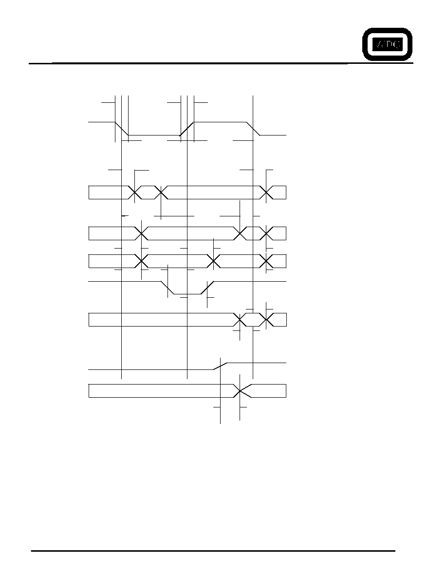
tF
tR
PHI2
tPWL
tPWH
tAH
tAH
see note 1
A0-A15. MLB,
R/W, SYNC, VPB
tADS
tACC
tDSR
Read Data
tDHR
tMDS
tDHR
Write Data
Write Data
tDHW
tPCS
tDHW
SOB
tPCH
tPCH
IRQB, NMIB
RDY, RESB
tPCS
SOB
DATA
tBVD
Figure 6-3 General Timing Diagram
Timing Notes:
1.
Timing measurement points are 50% VDD.
2.
PHI1O and PHI2O clock delay from PHI2 is no longer specified or tested and WDC recommends using an oscillator for system time base and PHI2
processor input clock.

The Western Design Center, Inc.
W65C02S Datasheet
The Western Design Center, Inc. W65C02S Datasheet 27
The page left blank intentionally
The Western Design Center, Inc.
W65C02S Datasheet
The Western Design Center, Inc. W65C02S Datasheet 28
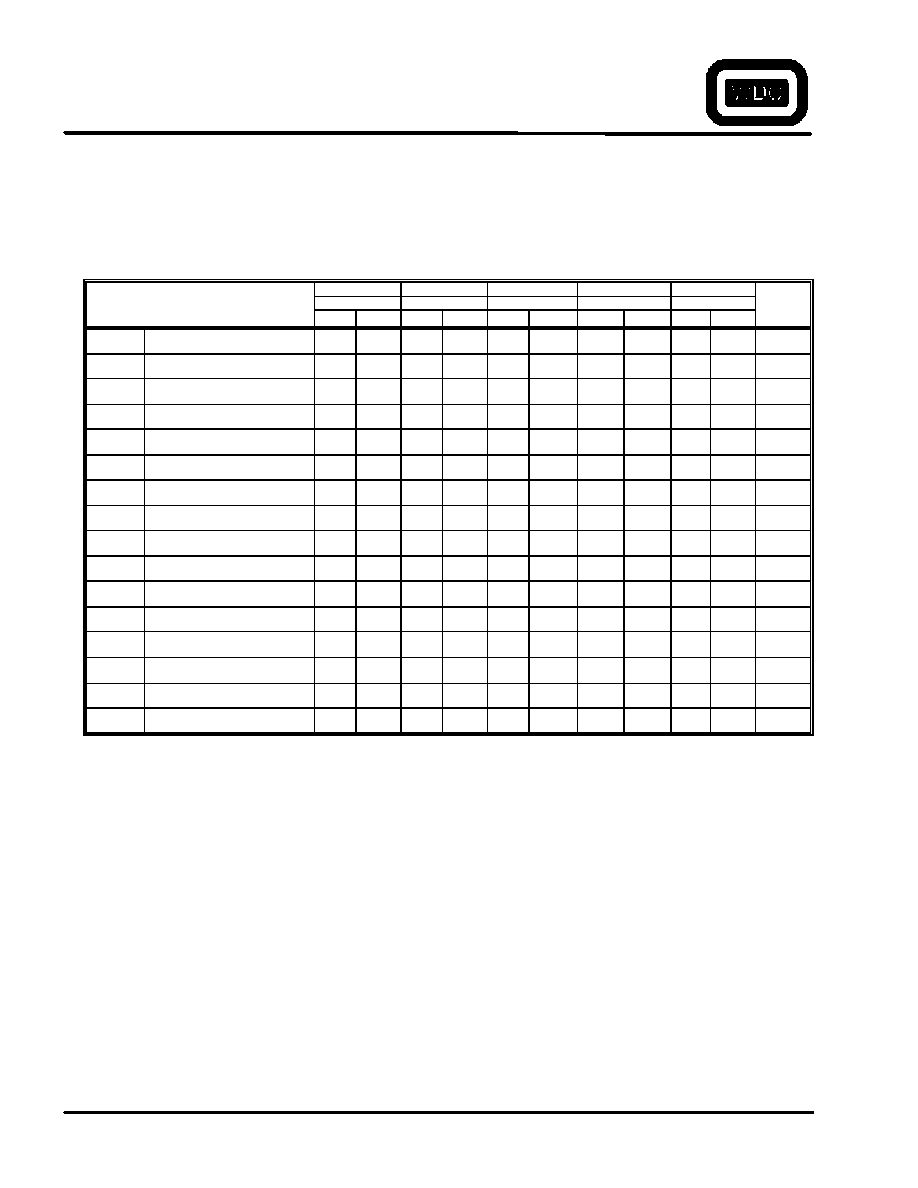
Table 6-4 Operation, Operation Codes and Status Register
Operation
# Immediate Data
~ NOT
^
AND
Processor Status Register (P)
*User Defined
v
OR
a
(a,x)
a,x
a,y
(a)
A
#
i
r
s
zp
(zp,x)
zp,x
zp,y
(zp)
(zp),y
7
6 5
4
3
2
1
0
Mnemomic
v
Exclusive OR
1
2
3
4
5
6
7
8
9
10
11
12
13
14
15
16
N
V 1
1
D
I
Z
C
ADC
A+M+C
A
6D
7D
79
69
65
61
75
72
71
N
V .
.
.
.
Z
C
AND
A^M
A
2D
3D
39
29
25
21
35
32
31
N
.
.
.
.
.
Z
.
ASL
C
7 6 5 4 3 2 1 0
0
0E
1E
0A
06
16
N
.
.
.
.
.
Z
C
BBR0
Branch on bit 0 reset
0F
.
.
.
.
.
.
.
.
BBR1
Branch on bit 1 reset
1F
.
.
.
.
.
.
.
.
BBR2
Branch on bit 2 reset
2F
.
.
.
.
.
.
.
.
BBR3
Branch on bit 3 reset
3F
.
.
.
.
.
.
.
.
BBR4
Branch on bit 4 reset
4F
.
.
.
.
.
.
.
.
BBR5
Branch on bit 5 reset
5F
.
.
.
.
.
.
.
.
BBR6
Branch on bit 6 reset
6F
.
.
.
.
.
.
.
.
BBR7
Branch on bit 7 reset
7F
.
.
.
.
.
.
.
.
BBS0
Branch on bit 0 set
8F
.
.
.
.
.
.
.
.
BBS1
Branch on bit 1 set
9F
.
.
.
.
.
.
.
.
BBS2
Branch on bit 2 set
AF
.
.
.
.
.
.
.
.
BBS3
Branch on bit 3 set
BF
.
.
.
.
.
.
.
BBS4
Branch on bit 4 set
CF
.
.
.
.
.
.
.
.
BBS5
Branch on bit 5 set
DF
.
.
.
.
.
.
.
.
BBS6
Branch on bit 6 set
EF
.
.
.
.
.
.
.
.
BBS7
Branch on bit 7 set
FF
.
.
.
.
.
.
.
.
BCC
Branch C = 0
90
.
.
.
.
.
.
.
.
BCS
Branch if C = 1
B0
.
.
.
.
.
.
.
.
BEQ
Branch if Z = 1
F0
.
.
.
.
.
.
.
.
BIT
A ^ M
2C
3C
89
24
34
M
7
M
6
.
.
.
Z
.
BMI
Branch if N = 0
30
.
.
.
.
.
.
.
.
BNE
Branch if Z = 0
D0
BPL
Branch if N = 0
10
.
.
.
.
.
.
.
.
BRA
Branch Always
80
.
.
.
.
.
.
.
.
The Western Design Center, Inc.
W65C02S Datasheet
The Western Design Center, Inc. W65C02S Datasheet
29
Operation
# Immediate Data
~ NOT
^
AND
Processor Status Register (P)
*User Defined
v
OR
a
(a,x)
a,x
a,y
(a)
A
#
i
r
s
zp
(zp,x)
zp,x
zp,y
(zp)
(zp
).y
7
6 5
4
3
2
1
0
Mnemomic
v
Exclusive OR
1
2
3
4
5
6
7
8
9
10
11
12
13
14
15
16
N
V 1
1
D
I
Z
C
BRK
Break
00
.
.
.
1
0
1
.
.
BVC
Branch if V = 0
50
.
.
.
.
.
.
.
.
BVS
Branch if V = 1
70
.
.
.
.
.
.
.
.
CLC
C
0
18
.
.
.
.
.
.
.
0
CLD
0
D
D8
.
.
.
.
0
.
.
.
CLI
0
1
58
.
.
.
.
.
0
.
.
CLV
0
V
B8
.
0
.
.
.
.
.
.
CMP
A-M
CD
DD
D9
C9
C5
C1
D5
D2
D1
N
.
.
.
.
.
Z
C
CPX
X-M
EC
E0
E4
N
.
.
.
.
.
Z
C
CPY
Y-M
CC
C0
C4
N
.
.
.
.
.
Z
C
DEC
Decrement
CE
DE
3A
C6
D6
N
.
.
.
.
.
Z
.
DEX
X-1
A
CA
N
.
.
.
.
.
Z
.
DEY
Y-1
Y
88
N
.
.
.
.
.
Z
.
EOR
A v M
A
4D
5D
59
49
45
41
55
52
51
N
.
.
.
.
.
Z
.
INC
Increments
EE
FE
1A
E6
F6
N
.
.
.
.
.
Z
.
INX
X+1
X
E8
N
.
.
.
.
.
Z
.
INY
Y+1
Y
C8
N
.
.
.
.
.
Z
.
JMP
Jump to new location
4C
7C
6C
.
.
.
.
.
.
.
.
JSR
Jump to Subroutine
20
N
.
.
.
.
.
Z
.
LDA
M
A
AD
BD
B9
A9
A5
A1
B5
B2
B1
N
.
.
.
.
.
Z
.
LDX
M
X
AE
BE
A2
A6
B6
N
.
.
.
.
.
Z
.
LDY
M
Y
AC
BC
A0
A4
B4
N
.
.
.
.
.
Z
.
LSR
0
7 6 5 4 3 2 1 0
C
4E
5E
4A
46
56
0
.
.
.
.
.
Z
C
NOP
No Operation
EA
.
.
.
.
.
.
.
.
The Western Design Center, Inc.
W65C02S Datasheet
The Western Design Center, Inc. W65C02S Datasheet
30
Operat ion
# Immediate Data
~ NOT
^
AND
Processor Status Register (P)
*User Defined
v
OR
a
(a,x)
a,x
a,y
(a)
A
#
i
r
s
zp
(zp,x)
zp,x
zp,y
(zp)
(zp),y
7
6 5 4
3
2
1
0
Mnemomic
v
Exclusiv e OR
1
2
3
4
5
6
7
8
9
10
11
12
13
14
15
16
N
V 1 1
D
I
Z
C
ORA
A V M
A
0D
1D
19
09
05
01
15
12
11
N
.
.
.
.
.
Z
.
PHA
A
Ms, S -1
S
48
.
.
.
.
.
.
.
.
PHP
P
Ms, S-1
S
08
.
.
.
.
.
.
.
.
PHX
X
Ms, S -1
S
DA
.
.
.
.
.
.
.
.
PHY
Y
Ms, S -1
S
5A
.
.
.
.
.
.
.
.
PLA
S + 1
S, Ms
A
68
N
.
.
.
.
.
Z
.
PLP
S + 1
S, Ms
P
28
N
V
.
1
D
I
Z
C
PLX
S + 1
S, Ms
X
FA
N
.
.
.
.
.
Z
.
PLY
S + 1
S, Ms
Y
7A
N
.
.
.
.
.
Z
.
RMB0
Reset Memory Bit 0
.
.
.
.
.
.
.
.
RMB1
Reset Memory Bit 1
.
.
.
.
.
.
.
.
RMB2
Reset Memory Bit 2
.
.
.
.
.
.
.
.
RMB3
Reset Memory Bit 3
.
.
.
.
.
.
.
.
RMB4
Reset Memory Bit 4
.
.
.
.
.
.
.
.
RMB5
Reset Memory Bit 5
.
.
.
.
.
.
.
.
RMB6
Reset Memory Bit 6
.
.
.
.
.
.
.
.
RMB7
Reset Memory Bit 7
.
.
.
.
.
.
.
ROL
C
7 6 5 4 3 2 1 0
C
2E
3E
2A
26
36
N
.
.
.
.
.
Z
C
ROR
C
7 6 5 4 3 2 1 0
C
6E
7E
6A
66
76
N
.
.
.
.
.
Z
C
RTI
Return from Interrupt
40
N
V
.
1.
D
I
Z
C
RTS
Return from Subroutine
60
.
.
.
.
.
.
.
.
SBC
A - M - (~C)
A
ED
FD
F9
E9
E5
E1
F5
F2
F1
N
V
.
.
.
.
Z
C
SEC
1
C
38
.
.
.
.
.
.
.
1
SED
1
D
F8
.
.
.
.
1
.
.
.
The Western Design Center, Inc.
W65C02S Datasheet
The Western Design Center, Inc. W65C02S Datasheet
31
Operation
# Immediate Data
~ NOT
^
AND
Processor Status Register (P)
*User Defined
v
OR
a
(a,x)
a,x
a,y
(a)
A
#
i
r
s
zp
(zp,x)
zp,x
zp,y
(zp)
(zp),y
7
6 5
4
3
2
1
0
Mnemomic
v
Exclusive OR
1
2
3
4
5
6
7
8
9
10
11
12
13
14
15
16
N
V 1
1
D
I
Z
C
SEI
1
I
78
.
.
.
.
.
1
.
.
SMB0
Set Memory Bit 0
87
.
.
.
.
.
.
.
.
SMB1
Set Memory Bit 1
97
.
.
.
.
.
.
.
.
SMB2
Set Memory Bit 2
A7
.
.
.
.
.
.
.
.
SMB3
Set Memory Bit 3
B7
.
.
.
.
.
.
.
.
SMB4
Set Memory Bit 4
C7
.
.
.
.
.
.
.
.
SMB5
Set Memory Bit 5
D7
.
.
.
.
.
.
.
.
SMB6
Set Memory Bit 6
E7
.
.
.
.
.
.
.
.
SMB7
Set Memory Bit 7
F7
.
.
.
.
.
.
.
.
STA
A
M
8D
9D
99
85
81
95
92
91
.
.
.
.
.
.
.
.
STP
STOP (1
PHI2)
DB
.
.
.
.
.
.
.
.
STX
X
M
8E
86
96
.
.
.
.
.
.
.
.
STY
Y
M
8C
84
94
.
.
.
.
.
.
.
.
STZ
00
M
9C
9E
64
74
.
.
.
.
.
.
.
.
TAX
A
Y
AA
N
.
.
.
.
.
Z
.
TAY
A
X
AB
N
.
.
.
.
.
Z
.
TRB
~A^M
M
1C
14
.
.
.
.
.
Z
.
TSB
AVM
M
0C
04
.
.
.
.
.
.
Z
.
TSX
S
X
BA
N
.
.
.
.
.
Z
.
TXA
X
A
8A
N
.
.
.
.
.
Z
.
TXS
X
S
9A
.
.
.
.
.
.
.
.
TYA
Y
A
98
N
.
.
.
.
.
Z
.
WAI
0
RDY
CB
.
.
.
.
.
.
.
.

The Western Design Center, Inc.
W65C02S Datasheet
The Western Design Center, Inc. W65C02S Datasheet 32
Table 6-5 Instruction Timing Chart
Address Mode
Note
Cycle
VPB
MLB
SYNC
Address Bus
Data Bus
RWB
1a. Absolute a
ADC, AND, BIT, CMP, CPX, CPY, EOR,
LDA, LDX, LDY, ORA, SBC, STA, STX,
STY, STZ
16 OpCodes, 3 bytes, 4&5 cycles
(6)
1
2
3
4
1
1
1
1
1
1
1
1
1
0
0
0
PC
PC+1
PC+2
AA
OpCode
AAL
AAH
Data
1
1
1
1/0
1b. Absolute (R-M-W) a
ASL, DEC, INC, LSR, ROL, ROR, TRB,
TSB
8 OpCodes, 3 bytes, 6 cycles
1
2
3
4
5
6
1
1
1
1
1
1
1
1
1
0
0
0
1
0
0
0
0
0
PC
PC+1
PC+2
AA
AA
AA
OpCode
AAL
AAH
Data
IO
Data
1
1
1
1
1
0
1c. Absolute (JUMP) a
JMP (4C)
1 OpCode, 3 bytes, 3 cycles
1
2
3
1
1
1
1
1
1
1
1
1
1
0
0
1
PC
PC+1
PC+2
New PC
OpCode
New PCL
New PCH
New OpCode
1
1
1
1
1d. Absolute (JUMP to subroutine) a
JSR (20)
1 OpCode, 3 bytes, 3 cycles
(different order from N6502)
1
2
3
4
5
6
1
1
1
1
1
1
1
1
1
1
1
1
1
1
1
1
0
0
0
0
0
1
PC
PC+1
S
S
S+1
PC+2
New PC
OpCode
New PCL
IO
PCH
PCL
New PCH
New OpCode
1
1
1
0
0
1
1
2. Absolute Indexed Indirect (a, x)
JMP (7C)
1 OpCode, 3 bytes, 6 cycles
(1)
1
2
3
4
5
6
1
1
1
1
1
1
1
1
1
1
1
1
1
1
1
1
0
0
0
0
0
1
PC
PC+1
PC+2
PC+2
AA+X
AA+X+1
New PC
OpCode
AAL
AAH
IO
New PCL
New PCH
OpCode
1
1
1
1
1
1
1
3a. Absolute , X a, x
ADC, AND, BIT, CMP, EOR, LDA, LDY,
ORA, SBC, STA, STZ
11 OpCodes, 3 bytes, 4,5 and 6 cycles
(1)
(6)
1
2
3
4
1
1
1
1
1
1
1
1
1
0
0
0
PC
PC+1
PC+2
AA+X
OpCode
AAL
AAH
Data
1
1
1
1/0
3b. Absolute, X(R-M-W) a, x
ASL, DEC, INC, LSR, ROL, ROR
6 OpCodes, 3 bytes, 7 cycles
(1)
1
2
3
4
5
6
7
1
1
1
1
1
1
1
1
1
1
1
0
0
0
1
0
0
0
0
0
0
PC
PC+1
PC+2
AAH,AAL+X
AA+X
AA+X+1
AA+X
OpCode
AAL
AAH
IO
Data
IO
Data
1
1
1
1
1
1
0
4. Absolute, Y a, y
ADC, AND, CMP, EOR, LDA, LDX, ORA,
SBC, STA
9 OpCodes, 3 bytes, 4,5 and 6 cycles
(1)
(6)
1
2
3
4
1
1
1
1
1
1
1
1
1
0
0
0
PC
PC+1
PC+2
AA+Y
OpCode
AAL
AAH
Data
1
1
1
1/0
5. Absolute Indirect (a)
JMP (6C)
1 OpCode, 3 bytes, 6 cycles
1
2
3
4
5
6
1
1
1
1
1
1
1
1
1
1
1
1
1
1
1
1
0
0
0
0
0
1
PC
PC+1
PC+2
PC+2
0,AA
0,AA+1
New PC
OpCode
AAL
AAH
IO
New PCL
New PCH
OpCode
1
1
1
1
1
1
1
6. Accumulator A
ASL, DEC, INC, LSR, ROL, ROR
6 OpCodes, 1 byte, 2 cycles
1
2
1
1
1
1
1
0
PC
PC+1
OpCode
IO
1
1
7. Immediate #
ADC, AND, BIT, CLR, CMP, CPY, CPX,
EOR, LDA, LDX, LDY, ORA, SBC
13 OpCodes, 2 bytes, 2 and 5 cycles
(6)
1
2
1
1
1
1
1
0
PC
PC+1
OpCode
ID
1
1
8a. Implied i
CLC, CLD, CLI, CLV, DEX, DEY, INX,
INY, NOP, SEC, SED, SEI, TAX. TAY,
TXA. TSX. TXS, TYA
18 OpCodes, 1 byte, 2 cycles
1
2
1
1
1
1
1
0
PC
PC+1
OpCode
IO
1
1
The Western Design Center, Inc.
W65C02S Datasheet
The Western Design Center, Inc. W65C02S Datasheet 33
Address Mode
Note
Cycle
VPB
MLB
SYNC
Address Bus
Data Bus
RWB
8b. Stop the Clock i
STP
1 OpCode, 1 byte, 3 cycles
RESB=1
RESB=0
RESB=0
RESB=1
1
2
3
1c
1b
1a
1
1
1
1
1
1
1
1
1
1
1
1
1
1
1
1
0
0
0
0
0
1
PC
PC+1
PC+1
PC+1
PC+1
PC+1
PC+1
OpCode
IO
IO
RES(BRK)
RES(BRK)
RES(BRK)
BEGIN
1
1
1
1
1
1
1
8c. Wait for Interrupt i
WAI
1 OpCode, 1 byte, 3 cycles
IRQB NMIB
(4)
1
2
3
1
1
1
1
1
1
1
1
1
1
0
0
1
PC
PC+1
PC+1
PC+1
OpCode
IO
IO
IRQ(BRK)
1
1
1
1
9a. Relative r
BCC, BCS, BEQ, BMI, BNE, BPL,
BRA, BVC, BVS
9 OpCodes, 2 bytes, 2,3 and 4 cycles
(2)
(3)
1
2
1
1
1
1
1
1
1
1
0
1
PC
PC+1
New PC
OpCode
Offset
OpCode
1
1
1
9b. Relative Bit Branch r
BBRx, BBSx
16 OpCodes, 3 bytes, 5,6 and 7 cycles
(2)
(3)
1
2
3
4
5
1
1
1
1
1
1
1
1
1
1
1
0
0
0
0
PC
PC+1
0,zp
PC+2
PC+Offset
OpCode
zp
Data
Offset
New OpCode
1
1
1
1
1
10a. Stack s
ABORTB, IRQB, NMIB, RESB
4 hardware interrupts, 0 bytes, 7 cycles
(5)
1
2
3
4
5
6
7
1
1
1
1
1
1
0
0
1
1
1
1
1
1
1
1
1
1
0
0
0
0
0
0
1
PC
PC
01,S
01,S-1
01,S-2
VA
VA+1
New PC
not used
not used
Return PCH
Return PCL
Return P
New PCL
New PCH
New OpCode
1
1
0
0
0
1
1
1
10b. Stack (Software Interrupts) s
BRK
1 OpCode, 2 bytes, 7 cycles
1
2
3
4
5
6
7
1
1
1
1
1
1
0
1
1
1
1
1
1
1
1
1
0
0
0
0
0
1
PC
PC+1
S
S-1
S-2
VA
VA+1
New PC
OpCode
not used
Return PCH
Return PCL+2
Return P
New PCL
New PCH
New OpCode
1
1
0
0
0
1
1
1
10c. Stack (Return from interrupt) s
RTI
1 OpCode, 1 byte, 6 cycles
1
2
3
4
5
6
1
1
1
1
1
1
1
1
1
1
1
1
1
1
1
1
0
0
0
0
0
1
PC
PC+1
S+1
S+2
S+3
PC+1
Return PC
OpCode
Not Used
Return P
Return PCL
Return PCH
IO
New OpCode
1
1
1
1
1
1
1
10d. Stack (Return from subroutine) s
RTS
1 OpCode, 1 byte, 6 cycles
1
2
3
4
5
6
1
1
1
1
1
1
1
1
1
1
1
1
1
1
1
1
0
0
0
0
0
1
PC
PC+1
PC+1
S+1
S+2
PC+1
Return PC
OpCode
not used
not used
Return PCL
Return PCH
IO
New OpCode
1
1
1
1
1
1
1
10e. Stack s
PHA, PHP, PHX, PHY
4 OpCodes, 1 byte, 3 cycles
1
2
3
1
1
1
1
1
1
1
1
1
1
0
0
1
PC
PC+1
S
PC+1
OpCode
not used
Register Value
New OpCode
1
1
0
1
10f. Stack s
PLA, PLP, PLX, PLY
4 OpCodes, 1 byte, 4 cycles
1
2
3
4
1
1
1
1
1
1
1
1
1
1
1
1
0
0
0
1
PC
PC+1
PC+1
S+1
PC+1
OpCode
not used
not used
Register Value
New OpCode
1
1
1
1
1
11a. Zero Page zp
ADC, AND, BIT, CMP, CPX, CPY,
EOR, LDA, LDX, LDY, ORA, SBC,
STA, STX, STY, STZ
16 OpCodes, 2 bytes, 3 and 4 cycles
1
2
3
1
1
1
1
1
1
1
1
1
1
0
0
1
PC
PC+1
0,zp
PC+2
OpCode
zp
Data
New OpCode
1
1
1/0
1
The Western Design Center, Inc.
W65C02S Datasheet
The Western Design Center, Inc. W65C02S Datasheet 34
Address Mode
Note
Cycle
VPB
MLB
SYNC
Address Bus
Data Bus
RWB
11b. Zero Page zp
ASL, DEC, INC, ROL, ROR, TRB, TSB
7 OpCodes
1
2
3
4
5
1
1
1
1
1
1
1
1
1
0
0
0
1
1
0
0
0
0
1
PC
PC+1
PC+1
zp
zp
PC+2
OpCode
zp
Data
not used
Data
New OpCode
1
1
1
1
0
1
11c. Zero Page zp
RMBx, SMBx
16 OpCodes, 2 bytes, 5 cycles
1
2
3
4
5
1
1
1
1
1
1
1
1
1
1
1
0
0
0
0
PC
PC+1
zp
zp
zp
OpCode
zp
Data
not used
Data
1
1
1
1
0
11d. Zero Page zp
BBRx, BBSx
16 OpCodes, 3 bytes, 5 cycles
1
2
3
4
5
1
1
1
1
1
1
1
1
1
1
1
1
1
1
0
0
0
0
1
PC
PC+1
zp
PC+2
PC+3
PC+2+0Offset
OpCode
zp
Data
Offset
not used
New OpCode
1
1
1
1
1
1
12. Zero Page Indexed Indirect (zp,x)
ADC, AND, CMP, EOR, LDA, ORA,
SBC, STA
8 OpCodes, 1 byte, 5 cycles
1
2
3
4
5
1
1
1
1
1
1
1
1
1
1
1
1
1
1
0
0
0
0
1
PC
PC+1
PC+1
0,zp+X
Indirect address
PC+1
OpCode
zp
not used
Indirect address
Data
New OpCode
1
1
1
1
1
1
13a. Zero Page Indexed with X zp,x
ADC, AND, BIT, CMP, EOR, LDA,
ORA, LDY, SBC, STA, STY, STZ
12 OpCodes, 1 byte, 4 cycles
1
2
3
4
1
1
1
1
1
1
1
1
1
1
1
1
0
0
0
1
PC
PC+1
PC+1
0,zp+X
PC+1
OpCode
zp
not used
Data
New OpCode
1
1
1
1/0
1
13b. Zerp Page Indexed with X zp,x
ASL, DEC, INC, LSR, ROL, ROR
6 OpCodes, 1 byte, 6 cycles
1
2
3
4
5
6
1
1
1
1
1
1
1
1
1
1
1
0
0
0
1
1
0
0
0
0
0
1
PC
PC+1
PC+1
0,zp+X
0,zp+X
0,zp+X
PC+1
OpCode
zp
not used
Data
not used
Data
New OpCode
1
1
1
1
1
0
1
14. Zero Page Indexed with Y zp,y
ADC, AND, CMP, EOR, LDA, LDX,
ORA, SBC, STA, STX
10 OpCodes, 1 byte, 4 cycles
1
2
3
4
1
1
1
1
1
1
1
1
1
1
1
1
0
0
0
1
PC
PC+1
PC+1
0,zp+Y
PC+1
OpCode
zp
not used
Data
New OpCode
1
1
1
1/0
1
15. Zero Page Indirect (zp)
ADC, AND, CMP, EOR, LDA, ORA,
SBC, STA
8 OpCodes, 1 byte, 4 cycles
1
2
3
4
1
1
1
1
1
1
1
1
1
1
1
1
0
0
0
1
PC
PC+1
0,zp
Indirect address
PC+1
OpCode
zp
Indirect address
Data
New OpCode
1
1
1
1/0
1
16.. Zero Page Indirect Indexed with y
(zp),y
ADC, AND, CMP, EOR, LDA, ORA,
SBC, STA
8 OpCodes, 1 byte, 4, 5 and 6 cycles
(6)
(1)
1
2
3
4
5
5a
1
1
1
1
1
1
1
1
1
1
1
1
1
0
0
0
0
0
PC
PC+1
0,zp
0,zp+1
Indirect address+y
PC+2
OpCode
zp
Indirect address HIGH
Indirect address LOW
Data
New OpCode
1
1
1
1
1/0
I

The Western Design Center, Inc.
W65C02S Datasheet
The Western Design Center, Inc. W65C02S Datasheet 35
Notes:
1. Add 1 cycle for indexing across page boundaries, or write. This cycle contains invalid addresses.
2. Add 1 cycle if branch is taken.
3. Add 1 cycle if branch is taken across page boundaries.
4. Wait at cycle 2 for 2 cycles after NMIB or IRQB active input.
5. RWB remains high during Reset.
6. Add 1 cycle for decimal mode
AAH
Absolute Address
PC
Program Counter
AAH
Absolute Address High
PCH
Program Counter High
AAL
Absolute Address Low
PCL
Program Counter Low
AAVH
Absolute Address Vector High
R-M -W
Read-Modify-Write
AAVL
Absolute Address Vector Low
REG
Register
C
Accumulator
S
Stack Address
DEST
Destination
SRC
Source
ID
Immediate Data
SO
Stack Offset
IO
Internal Operation
V
Vector Address
P
Status Register
x,y
Index Register
zp
Zero Page Address

The Western Design Center, Inc.
W65C02S Datasheet
The Western Design Center, Inc. W65C02S Datasheet 36
7
CAVEATS
Table 7-1 Microprocessor Operational Enhancements
Function
NMOS 6502
W65C02S
Indexed addressing across page
boundary
Extra read of invalid address.
Extra read of last instruction byte.
Execution of invalid OpCodes.
Some terminate only by reset.
Results are undefined.
All are NOP's (reserved for future use).
OpCode Bytes Cycles
02,22,42,62,82 2 2
C2, E2
X3,OB-BB,EB,FB 1
1
44
2
3
54,D4,F4
2
4
5C
3
8
DC,FC
3
4
Jump indirect, operand = XXFF.
Page address does not increment.
Page address increments, one additional
cycle.
Read/Modify/Write instruction at
effective address.
One read and two write cycles.
Two read and one write cycle.
Decimal flag.
Indeterminate after reset.
Initialized to binary mode (D=0) after reset
and interrupts.
Flags after decimal operation.
Invalid N, V and Z flags.
Valid flags. One additional cycle.
Interrupt after fetch of BRK
instruction
Interrupt vector is loaded; BRK
vector is ignored.
BRK is executed, and then interrupt is
executed.
Ready.
Input.
Bi-directional, WAI instruction pulls low.
Read/Modify/Write instructions
absolute indexed in same page.
Seven cycles.
Six cycles.
Oscillator.
Requires external active components. Crystal or RC network will oscillate when
connected between PHI2 and PHI10.
Assertion of Ready (RDY) during
write operations.
Ignored.
Stops processor during PHI2, and WAI
instruction pulls RDY low.
Clock inputs.
PHI2 is the only required clock.
PHI2 is the only required clock.
Unused input-only pins.
Must be tied to VDD.
Must be tied to VDD.
The BRK instruction for both the NMOS 6502 and 65C02 is a 2 byte instruction. The NMOS and CMOS devices
simply skips the second byte (i.e. doesn't care about the second byte) by incrementing the program counter twice.
It is important to realize that if a return from interrupt is used it will return to the location after the second or
signature byte.
The Western Design Center, Inc.
W65C02S Datasheet
The Western Design Center, Inc. W65C02S Datasheet 37
MEMORY BUS
EPROM
RAM
I/O
MATRIX
JTAG
OSCILLATOR
RESET
CIRCUIT
PHI2
RESB
MPU
CONTROL BUS
ADDRESS BUSS
DATA BUSS
CHIP SET
PLD
PORTS
PC
PARALLEL PORT
I/O
I/O
8
W65C02DB DEVELOPER BOARD AND
IN-CIRCUIT EMULATOR (ICE)
The W65C02DB is used for W65C02 core microprocessor System-Chip Development, W65C02S (chip) System
Development, or Embedded W65C02DB (board) Development.
PROGRAMABLE I/O BUSS

The Western Design Center, Inc.
W65C02S Datasheet
The Western Design Center, Inc. W65C02S Datasheet 38
8.1
Features:
W65C02S 8-bit MPU, total access to all control lines, Memory Bus, Programmable I/O Bus, PC Interface, 20 I/O lines, easy
oscillator change, 32K SRAM, 32K EPROM, W65C22S Versatile Interface Adapter VIA peripheral chip, on-board matrix,
CPLD for Memory map decoding, hardware breakpoints and ASIC design.
The CPLD chip is a XILINX XC95108 for changing the chip select and I/O functions if required. To change the CPLD chip
to suit your own setup, you need XILINX Data Manager for the XC95108 CPLD chip. The W65C02DB includes an on-
board programming header for JTAG configuration. For more details refer to the circuit diagram. The on-board W65C02S
and the W65C22S devices have measurement points for core power consumption. Power input is provided by an optional
power board which plugs into the 10 pin power header.
An EPROM programmer or an EPROM emulator is required to reprogram the EPROM. WDC's (W65SDS) Software
Development System includes a W65C02S Assembler and Linker, W65C02S C-Compiler and Optimizer, and W65C02S
Simulator/Debugger. WDC's PC IO daughter board can be used to connect the Developer Board to the parallel port of a PC
for In-Circuit Debugging.
8.2
Memory map:
CS1B:
8000-FFFF
EPROM (27C256)
CS3B:
0000-00EF & 0100-7FFF
SRAM (62C256)
CS2B:
00F0-00FF
VIA(W65C22S)
8.3
Cross-Debugging Monitor Program
The Cross-Debugging Monitor Programs of the Developer Boards are located in the directory
<drive>:\WDC_SDS\DEBUG\WDCMON\
This directory contains the source and the batch files for all of the monitor programs. These programs can be burned into an
EPROM and used with the WDC evaluation boards (Developer Boards) and the WDC IO (or ZIO-1) daughter board to
interface to the parallel port of a PC. Then, the WDCDB.EXE debugger can be used to download programs, single step, set
breakpoints, examine memory, etc for In-Circuit Debugging (ICD).
The monitors have been designed to run correctly with a W65C02 MPU (WDCMON_1), W65C816 MPU (WDCMON_2),
W65C134 MCU (WDC134), or W65C265 MCU (WDC265). It detects the appropriate CPU type on RESET and operates
accordingly.
8.4
BUILDING
The batch files assemble the program and link it producing Motorola S-Record output. This can be changed by using a
different option with the WDCLN linker

The Western Design Center, Inc.
W65C02S Datasheet
The Western Design Center, Inc. W65C02S Datasheet 39
9
HARD CORE MODEL
9.1
Features of the W65C02S Hard Core Model
∑
The W65C02S core uses the same instruction set as the W65C02S.
∑
The only functional difference between the W65C02S and W65C02S core is the RDY pin. The W65C02S RDY pin is
bi-directional utilizing an active pull-up. The W65C02S core RDY function is split into 2 pins, RDY, WAITN and
WAITP. The WAITN output goes low and WAITP goes high when a WAI instruction is executed.
∑
The ESD and latch-up buffers have been removed.
∑
The output from the core is the buffer N-channel and the P-channel transistor drivers.
∑
The following inputs, if not used, must be pulled to the high state: RDY, IRQB, NMIB, BE and SOB.
∑
The timing of the W65C02S core is the same as the W65C02S.
10
SOFT CORE RTL MODEL
10.1
W65C02 Synthesizable RTL-Code in Verilog HDL
The RTL-Code (Register Transfer Level) in Verilog is a synthesizable model. The behavior of this model is equivalent to
the original W65C02S hardcore. The W65C02 RTL-Code is available as the core model and the W65C02S standard chip
model. The standard chip model includes the soft-core and the buffer ring in RTL-Code.
The Western Design Center, Inc.
W65C02S Datasheet
The Western Design Center, Inc. W65C02S Datasheet 40
ORDERING INFORMATION
W65C02S6PL-14
Description
W65C
W65C = standard product
Product Identification Number
02S
Foundry Process
6
Blank = 1.2u
8=.8u, 6=.6u
Package
PL
P = Plastic Dual-In-Line, 40 pins
PL = Plastic Leaded Chip Carrier, 44 pins
Q = Quad Flat Pack, 44 pins
Temperature/Processing
Blank = -40
∞
C to + 85
∞
C (PLCC and QFP) 0
∞
C to 70
∞
C (DIP)
Speed Designator
-14
-14 = 14MHz
____________________________________________________________________________________
To receive general sales or technical support on standard product or information about our module library licenses,
contact us at:
The Western Design Center, Inc.
2166 East Brown Road
Mesa, Arizona 85213 USA
Phone: 480-962-4545 Fax: 480-835-6442
information@westerndesigncenter.com
www.westerndesigncenter.com
_______________________________________________________________________________________
WARNING: MOS CIRCUITS ARE SUBJECT TO DAMAGE FROM STATIC DISCHARGE
Internal static discharge circuits are provided to minimize part damage due to environmental static electrical charge
build-ups. Industry established recommendations for handling MOS circuits include:
1. Ship and store product in conductive shipping tubes or conductive foam plastic. Never ship or store product in
non-conductive plastic containers or non-conductive plastic foam material.
2. Handle MOS parts only at conductive work stations.
3. Ground all assembly and repair tools.