
The Western Design Center, Inc.
W65C22S Data Sheet
The
Western
Design
Center
W65C22S
1
W65C22S
Versatile Interface Adapter (VIA)
DATA SHEET

The Western Design Center, Inc.
W65C22S Data Sheet
The
Western
Design
Center
W65C22S
2
WDC reserves the right to make changes at any time without notice in order to improve design and supply the
best possible product. Information contained herein is provided gratuitously and without liability, to any user.
Reasonable efforts have been made to verify the accuracy of the information but no guarantee whatsoever is
given as to the accuracy or as to its applicability to particular uses. In every instance, it must be the
responsibility of the user to determine the suitability of the products for each application. WDC products are
not authorized for use as critical components in life support devices or systems. Nothing contained herein shall
be construed as a recommendation to use any product in violation of existing patents or other rights of third
parties. The sale of any WDC product is subject to all WDC Terms and Conditions of Sales and Sales Policies,
copies of which are available upon request.
Copyright
1981-2006 by The Western Design Center, Inc. All rights reserved, including the right of
reproduction, in whole, or in part, in any form.

The Western Design Center, Inc.
W65C22S Data Sheet
The
Western
Design
Center
W65C22S
3
TABLE OF CONTENTS
1. SECTION 1 W65C22S FUNCTION DESCRIPTION....................................................................... 8
1.1.
Peripheral Data Ports ................................................................................................................................8
1.2.
Data Transfer - Handshake Control ......................................................................................................10
1.3.
Read Handshake Control. .......................................................................................................................11
1.4.
Write Handshake Control. ......................................................................................................................12
1.5.
Timer 1 Operation ...................................................................................................................................14
1.6.
Timer 1 One-Shot Mode ..........................................................................................................................17
1.7.
Timer 1 Free-Run Mode..........................................................................................................................18
1.8.
Timer 2 Operation. ..................................................................................................................................19
1.9.
Timer 2 One-Shot Mode ..........................................................................................................................19
1.10.
Timer 2 Pulse Counting Mode. ...............................................................................................................20
1.11.
Shift Register Operation..........................................................................................................................20
1.12.
Shift Register Input Modes. ....................................................................................................................21
1.12.1
Shift Register Disabled (000).......................................................................................................................... 21
1.12.2
Shift In - Counter T2 Control (001) ................................................................................................................ 22
1.12.3
Shift In - PHI2 Clock Control (010) ................................................................................................................. 22
11.12.2.
Shift In - External CB1 Clock Control (011) .................................................................................................. 23
1.13.
Shift Register Output Modes...................................................................................................................23
1.13.1
Shift Out - Free Running at T2 Rate (100)...................................................................................................... 23
1.13.2
Shift Out - T2 Control (101) ............................................................................................................................ 24
1.13.3
Shift Out - PHI2 Clock Control (110) .............................................................................................................. 24
1.13.4
Shift Out - External CB1 Clock Control (111)................................................................................................ 25
1.14.
Interrupt Operation..................................................................................................................................25
2. SECTION 2 PIN FUNCTION DESCRIPTION .............................................................................. 28
2.1
Peripheral Data Port A Control Lines. (CA1, CA2) .............................................................................31
2.2
Peripheral Data Port B Control Lines. (CB1, CB2)..............................................................................31
2.3
Chip Select (CS1, CS2B)..........................................................................................................................32
2.4
Data Bus. (D0-D7) ....................................................................................................................................32
2.5
Interrupt Request. (IRQB)......................................................................................................................32
2.6
Peripheral Data Port A(PA0-PA7) .........................................................................................................32
2.7
Peripheral Data Port B (PB0-PB7).........................................................................................................33
2.8
Phase 2 Internal Clock. (PHI2) ...............................................................................................................34
2.9
Reset (RESB) ...........................................................................................................................................34
2.10
Register Select. (RS0-RS3) ......................................................................................................................34
2.11
RWB (Read/Write) ...................................................................................................................................34
2.12
VDD and VSS. ..........................................................................................................................................34

The Western Design Center, Inc.
W65C22S Data Sheet
The
Western
Design
Center
W65C22S
4
3. SECTION 3 TIMING, AC AND DC CHARACTERISTICS ........................................................... 35
3.1
Absolute Maximum Ratings...................................................................................................................35
3.2
DC Characteristics. TA=-40
∞C to
+85C
∞..............................................................................................36
3.3
AC Characteristic TA=-40
∞C to
+85
∞C ...............................................................................................37
4. SECTION 4 CAVEATS ..................................................................................................................... 44
4.1
Caveats ......................................................................................................................................................44
5. SECTION 5 HARD CORE MODEL ................................................................................................ 45
Application Notes ..................................................................................................................................................45
6. SECTION 6 ORDERING INFORMATION .................................................................................... 46

The Western Design Center, Inc.
W65C22S Data Sheet
The
Western
Design
Center
W65C22S
5
Table of Figures
FIGURE 1-1 READ HANDSHAKE OPERATION (PA ONLY).......................................................................................... 11
FIGURE 1-2 WRITE HANDSHAKE (PA AND PB) ............................................................................................................ 12
FIGURE 1-3 ONE-SHOT MODE (TIMER 1 AND TIMER 2) ............................................................................................... 17
FIGURE 1-4 FREE-RUN MODE (TIMER 1) ....................................................................................................................... 18
FIGURE1-5 PULSE COUNTING MODE (TIMER 2) .......................................................................................................... 20
FIGURE 1-6 SHIFT IN - COUNTER T2 CONTROL ........................................................................................................... 22
FIGURE-1-7 SHIFT IN - PHI2 CLOCK CONTROL ............................................................................................................ 22
FIGURE 1-8 SHIFT IN - EXTERNAL CB1 CLOCK CONTROL TIMING ........................................................................ 23
FIGURE 1-9 SHIFT OUT - FREE RUNNING T2 RATE TIMING...................................................................................... 23
FIGURE 1-10 SHIFT OUT - T2 CONTROL TIMING.......................................................................................................... 24
FIGURE 1-11 SHIFT OUT - PHI2 CONTROL TIMING...................................................................................................... 24
FIGURE 1-12 SHIFT OUT - EXTERNAL CB1 CLOCK CONTROL TIMING .................................................................. 25
FIGURE 2-1 PIN PLCC PINOUT.......................................................................................................................................... 28
FIGURE 2-2 W65C22S 40 PIN PDIP PINOUT .................................................................................................................... 29
FIGURE 2-3 W65C22S 44 PIN QFP PINOUT...................................................................................................................... 30
FIGURE 2-4 PORT A BUFFER (PA0-PA7, CA2) ................................................................................................................ 33
FIGURE 2-5 PORT B BUFFER (PB0-PB7, CB1, AND CB2) .............................................................................................. 33
FIGURE 3-1 IDD VS VDD..................................................................................................................................................... 36
FIGURE 3-2 READ TIMING................................................................................................................................................. 39
FIGURE 3-3 WRITE TIMING ................................................................................................................................................ 39
FIGURE 3-4 READ HANDSHAKE, PULSE MODE (CA2).................................................................................................. 40
FIGURE 3-5 READ HANDSHAKE, HANDSHAKE MODE TIMING (CA2) .................................................................... 40
FIGURE 3-6 WRITE HANDSHAKE, PULSE MODE TIMING (CA2, CB2) ........................................................................ 41
FIGURE 3-7 WRITE HANDSHAKE, HANDSHAKE MODE TIMING (CA2, CB2) ............................................................ 41
FIGURE 3-8 PERIPHERAL DATA, INPUT LATCHING TIMING ...................................................................................... 42
FIGURE 3-9 DATA SHIFT OUT, INTERNAL OR EXTERNAL SHIFT CLOCK TIMING ................................................. 42
FIGURE 3-10 DATA SHIFT IN, INTERNAL OR EXTERNAL SHIFT CLOCK TIMING ................................................ 42
FIGURE 3-11 PULSE COUNT INPUT TIMING.................................................................................................................. 43
FIGURE 3-12 TEST LOAD (ALL DYNAMIC PARAMETERS) ........................................................................................ 43
FIGURE 4-1 IRQB DIFFERENCE ........................................................................................................................................ 44
FIGURE 4-2 HIGH RESISTANCE BUS HOLDING DEVICE ............................................................................................ 44

The Western Design Center, Inc.
W65C22S Data Sheet
The
Western
Design
Center
W65C22S
6
TABLE OF TABLES
TABLE 1-1 W65C22S MEMORY MAP OF INTERNAL REGISTERS ...................................................................................... 8
TABLE 1-2 ORB, IRB OPERATION FOR REGISTER 0 ($00).................................................................................................... 9
TABLE 1-3 ORA, IRA OPERATION FOR REGISTER 1 ($01) ................................................................................................. 10
TABLE 1-4 DDRB, DDRA OPERATION ($02,$03)................................................................................................................... 10
TABLE 1-5 CA1, CA2, CB1, CB2 CONTROL1 ($0C).............................................................................................................. 12
TABLE 1-6 T1 COUNTER FORMAT AND OPERATION1 ($04,$05) ...................................................................................... 15
TABLE 1-7 T1 LATCH FORMAT AND OPERATION1 ($06,$07)............................................................................................ 15
TABLE 1-8 AUXILIARY CONTROL REGISTER FORMAT AND OPERATION ($0B).......................................................... 16
TABLE 1-9 T2 COUNTER FORMAT AND OPERATION1 ($08,$09).................................................................................... 19
TABLE 1-10 SHIFT REGISTER AND AUXILIARY CONTROL REGISTER CONTROL ($0A).......................................... 21
TABLE 1-11 INTERRUPT FLAG REGISTER ($0D) ............................................................................................................... 26
TABLE 1-12 INTERRUPT ENABLE REGISTER ($0E)........................................................................................................... 27
TABLE 2-1 PIN FUNCTION TABLE........................................................................................................................................ 31
TABLE 3-1 ABSOLUTE MAXIMUM RATINGS..................................................................................................................... 35
TABLE 3-2 DC CHARACTERISTICS ....................................................................................................................................... 36
TABLE 3-3 W65C22S AC CHARACTERISTICS ...................................................................................................................... 37
TABLE 3-4 W65C22S AC........................................................................................................................................................... 38

The Western Design Center, Inc.
W65C22S Data Sheet
The
Western
Design
Center
W65C22S
7
INTRODUCTION
The W65C22S Versatile Interface Adapter (VIA) is a flexible I/O device for use with the W65C series
microprocessor family. The W65C22S includes functions for programmed control of two peripheral ports (Ports A
and B). Two program controlled 8-bit bi-directional peripheral I/O ports allow direct interfacing between the
microprocessor and selected peripheral units. Each port has input data latching capability. Two programmable Data
Direction Registers (A and B) allow selection of data direction (input or output) on an individual line basis. Also
provided are two programmable 16-bit Interval Timer/Counters with latches. Timer 1 may be operated in a
One-Shot Interrupt Mode with interrupts on each count-to-zero, or in a Free-Run Mode with a continuous series of
evenly spaced interrupts. Timer 2 functions as both an interval and pulse counter. Serial Data transfers are provided
by a serial-to-parallel/parallel-to-serial shift register. Application versatility is further increased by various control
registers, including an Interrupt Flag Register, an Interrupt Enable Register and two Function Control Registers. The
IRQB output is an open drain.
KEY FEATURES OF THE W65C22S
∑ Advanced CMOS process technology for low
power consumption
∑ Compatible with NMOS 6522 devices
∑ Low power consumption
∑ Two 8-bit, bi-directional peripheral I/O Ports
∑ Two 16-bit programmable Interval Timer/Counters
∑ Serial bi-directional peripheral I/O Port
∑ Enhanced "handshake" feature
∑ Latched Input/Output Registers on both I/O
Ports
∑ Programmable Data Direction Registers
∑ TTL compatible I/O peripheral lines
∑ Single 1.8V to 5V power supply
∑ Bus compatible with high-speed W65C02S and
W65C816S
∑ Register and Chip Selects specified for
multiplexed operation
Figure 1 W65C22S Internal Architecture Block Diagram
DATA
BUS
BUFFERS
ACCESS
CONTROL
LOGIC
RSO
RS1
RS2
RS3
CS1
CS2B
RESB
PHI2
R/WB
DATA
BUS
INTERUPT CONTROL
∑FLAGS (IFR)
∑ENABLE (IER)
FUNCTION CONTROL
∑PERIPHERAL (PCR)
∑AUXILIARY (ACR)
TIMER 1
∑LATCHES
(T1L-H, T1L-L)
∑COUNTERS
(T1C-H, T1C-L)
TIMER 2
∑LATCH (T2L-L)
∑
COUNTERS
(T2C-H, T2C-L)
PORT B REGISTERS
∑
INPUT LATCH (IRB)
∑
OUTPUT (ORB)
∑DATA DIRECTION (DDRB)
SERIAL DATA
SHIFT REGISTER
(SR)
HANDSHAKE CONTROL
∑PORT A
∑PORT B
PORT A REGISTERS
∑INPUT LATCH (IRA)
∑OUTPUT (ORA)
∑
DATA DIRECTION (DDRA)
PORT
A
BUFFERS
(PA)
PORT
B
BUFFERS
(PB)
IRQB
PORT A
BUS
CA2
CA1
CB2
CB1
PORT B
BUS

The Western Design Center, Inc.
W65C22S Data Sheet
The Western Design Center
W65C22S
8
1. SECTION 1 W65C22S FUNCTION DESCRIPTION
Table 1-1 W65C22S Memory Map of Internal Registers
Register
Number
RS Coding
Register
Designation
Description
RS3
RS2
RS1
RS0
Write
Read
0
0
0
0
0
ORB/IRB
Output Register "B"
Input Register "B"
1
0
0
0
1
ORA/IRA
Output Register "A"
Input Register "A"
2
0
0
1
0
DDRB
Data Direction Register "B"
3
0
0
1
1
DDRA
Data Direction Register "A"
4
0
1
0
0
T1C-L
T1 Low-Order Latches
T1 Low-Order Counter
5
0
1
0
1
T1C-H
T1 High-Order Counter
6 0
1
1
0
T1L-L
T1
Low-Order
Latches
7
0
1
1
1
T1L-H
T1 High-Order Latches
8
1
0
0
0
T2C-L
T2 Low-Order Latches
T2 Low-Order Counter
9
1
0
0
1
T2C-H
T2 High-Order Counter
A 1
0
1
0
SR
Shift
Register
B
1
0
1
1
ACR
Auxiliary Control Register
C
1
1
0
0
PCR
Peripheral Control Register
D
1
1
0
1
IFR
Interrupt Flag Register
E
1
1
1
0
IER
Interrupt Enable Register
F
1
1
1
1
ORA/IRA
Same as Reg 1 except no "Handshake"
1.1. Peripheral Data Ports
Bo
th PA and PB operate in conjunction with a Data Direction Register (DDRA or DDRB). Under program control, the
DDRA and DDRB specify which lines within the port bus are to be designated as inputs or outputs. A Logic 0 in any bit
position of the register will cause the corresponding line to serve as an input, while a Logic 1 will cause the line to serve as
an output.
When a line is programmed as an output, it is controlled by a corresponding bit in the Output Register (ORA & ORB). A
Logic 1 in the ORA or ORB will cause the corresponding output line to go high, while a Logic 0 will cause the line to go
low. Under program control, data is written into the ORA or ORB bit positions corresponding to the output lines which
have been programmed as outputs. Should data be written into bit positions corresponding to lines which have been
programmed as input, the output lines will be unaffected.

The Western Design Center, Inc.
W65C22S Data Sheet
The
Western
Design
Center
W65C22S
9
When reading PA or PB, the contents of the corresponding Input Register (IRA or IRB) is transferred onto the Data Bus.
When the input latching feature is disabled, IRA will reflect the logic levels present on the PA bus lines. However, with
input latching enabled and the selected active transition on Peripheral A Control 1 (CA1) having occurred, IRA will
contain the data present on the PA bus lines at the time of the transition. In this case, once IRA has been read, it will
appear transparent, reflecting the current state of the PA bus lines until the next CA1 latching transition.
With respect to IRB, it operates similar to IRA except that for those PB bus lines that have been programmed as outputs,
there is a difference. When reading IRA, the logic level on the bus line determines whether a Logic 1 or 0 is sensed.
However, when reading IRB, the logic level stored in ORB is the logic level sensed. For this reason, those outputs which
have large loading effects may cause the reading of IRA to result in the reading of a Logic 0 when a 1 was actually
programmed, and reading Logic 1 when a 0 was programmed. However, when reading IRB, the logic level read will be
correct, regardless of loading on the particular bus line.
For information on formats and operation of the PA and PB registers, see Tables 1-2, 1-3 & 1-4. Note that the input
latching modes are controlled by the Auxiliary Control Register (See Table 1-8).
Table 1-2 ORB, IRB Operation for Register 0 ($00)
7 6 5 4 3 2 1 0 ORB,IRB
PB7 PB6 PB5 PB4 PB3 PB2 PB1 PB0
Pin Data Direction
Selection
WRITE
READ
DDRB="1" (Output)
MPU writes Output Level (ORB)
MPU reads output register bit in ORB. Pin
level has no effect.
DDRB="0" (Input)
(Input latching disabled)
MPU writes onto ORB, but no
effect on pin level, until DDRB
changed.
MPU reads input level
on PB pin.
DDRB="0" (Input)
(Input latching enabled)
MPU reads IRB bit, which is the level of the
PB pin at the time of the last CB1 active
transition.

The Western Design Center, Inc.
W65C22S Data Sheet
The
Western
Design
Center
W65C22S
10
Table 1-3 ORA, IRA Operation for Register 1 ($01)
7 6 5 4 3 2 1 0
ORA,IRA
PA7 PA6 PA5 PA4 PA3 PA2 PA1 PA0
Pin Data Direction
Selection
WRITE
READ
DDRA="1" (Output)
(Input latching disabled)
MPU writes Output Level
(ORA)
MPU reads level on PA pin.
DDRA="1" (Output)
(Input latching enabled)
MPU reads IRA bit which is the level of
the PA pin at the time of the last CA1
active transition.
DDRA="0" (Input)
(Input latching disabled)
MPU writes into ORA, but no effect
on pin level, until DDRA changed.
MPU read level on PA pin.
DDRA="0 (Input)
(Input latching enabled)
MPU reads IRA bit which is the level of
the PA pin at the time of the last CA1
active transition.
Table 1-4 DDRB, DDRA Operation ($02,$03)
7 6 5 4 3 2 1 0
DDRB,DDRA
PB7/PA7 PB6/PA6 PB5/PA5 PB4/PA4 PB3/PA3 PB2/PA2 PB1/PA1 PB0/PA0
"0" Associated PB/PA pin is an input (high impedance)
"1" Associated PB/PA pin is an output, whose level is determined by ORB/ORA Bit.
1.2. Data Transfer - Handshake Control
A powerful feature of the W65C22S is its ability to provide absolute control over data transfers between the
microprocessor and peripheral devices. This control is accomplished by way of "handshake" lines. PA lines
Peripheral A Control 1,2 (CA1, CA2) handshake data transfers on both Read and Write operations, while PB lines
Peripheral B Control 1,2 (CB1, CB2) handshake data on Write operations only.

The Western Design Center, Inc.
W65C22S Data Sheet
The
Western
Design
Center
W65C22S
11
1.3. Read Handshake Control.
Read Handshaking provides effective control of data transfers from a peripheral device to the microprocessor. To
accomplish the Read Handshake, the peripheral device generates a Data Ready signal to the W65C22S that indicates
valid data is present on PA or PB. In most cases, this Data Ready signal will interrupt the microprocessor, which
will then read the data and generate a Data Taken signal. Once the peripheral senses the Data Taken signal, new
data will be placed on the bus. This process continues until the data transfer is complete.
Automatic Read Handshaking applies to PA only. The Data Ready signal is transmitted by the peripheral device
over the CA1 interrupt line, while the Data Taken signal is generated and transmitted to the peripheral device over
the CA2 line. When the Data Ready signal is received, it sets an internal flag in the Interrupt Flag Register (IFR).
This flag may interrupt the microprocessor or it may be polled under program control. As an option, the Data Taken
signal may be either a pulse or a level. In either case, it is set to a Logic 0 by the microprocessor and is set by the
next Data Ready signal, see Figure 1-1.
Figure 1-1 Read Handshake Operation (PA Only)
PHI2
"DATA READY"
(CA1)
IRQB OUTPUT
READ IRA OPERATION
"DATA TAKEN"
HANDSHAKE MODE (CA2)
"DATA TAKEN"
PULSE MODE (CA2)

The Western Design Center, Inc.
W65C22S Data Sheet
The
Western
Design
Center
W65C22S
12
1.4. Write Handshake Control.
The Write Handshake operation is similar to Read Handshaking. For Write Handshaking, however, the W65C22S
generates the Data Ready signal and the peripheral device must generate the Data Taken return signal. Note that
Write Handshaking may occur on both PA and PB. For a Write Handshake, CA2 or CB2 serve as the Data Ready
output and can operate in either the Handshake Mode or the Pulse Mode. The Data Taken signal is received the
CA1 or CB1. The Data Taken signal sets a flag in the Interrupt Flag Register and clears the Data Ready output
signal, see Figure 1-2.
Note that the selection of Read or Write Handshake operating modes for CA1, CA2, CB1 and CB2 is accomplished
by the Peripheral Control Register (PCR). See Table 1-5.
Figure 1-2 Write Handshake (PA and PB)
Table 1-5 CA1, CA2, CB1, CB2 Control1 ($0C)
7 6 5 4 3 2 1 0 PCR
CB2 Control
CB1
Control
CA2 Control
CA1
Control
PHI2
WRITE ORA, ORB
OPERATION
"DATA READY"
HANDSHAKE MODE
(CA2, CB2)
"DATA READY"
PULSE MODE
(CA1.CB1)
"DATA TAKEN"
(CA1,CB1)
IRQB OUPUT

The Western Design Center, Inc.
W65C22S Data Sheet
The
Western
Design
Center
W65C22S
13
CB2 Control
7 6 5 Operation
0
0
0
Input-negative active edge
0
0
1
Independent interrupt input-negative edge*
0
1
0
Input-positive active edge
0
1
1
Independent interrupt input-positive edge*
1 0 0 Handshake
output
1 0 1 Pulse
output
1 1 0 Low
output
1 1 1 High
output
CB1 Interrupt Control
0 = Negative Active Edge
1 = Positive Active Edge
CA2 Control
3
2 1 Operation
0
0
0
Input-negative active edge
0
0
1
Independent interrupt input-negative edge*
0
1
0
Input-positive active edge
0
1
1
Independent interrupt input-positive edge*
1 0 0 Handshake
output
1 0 1 Pulse
output
1 1 0 Low
output
1 1 1 High
output
CA1 Interrupt Control
0 = Negative Active Edge
1 = Positive Active Edge

The Western Design Center, Inc.
W65C22S Data Sheet
The
Western
Design
Center
W65C22S
14
* If the CA2/CB2 control in the PCR is selected as "independent" interrupt input, then reading or writing the output register
ORA/ORB will not clear the flag bit. Instead, the bit must be cleared by writing into the IFR, as described previously.
1.5. Timer 1 Operation
Interval Timer 1 (T1) consists of two 8-bit latches and a 16-bit counter. The latches serve to store data which is to
be loaded into the counter. Once the counter is loaded under program control, it decrements at Phase 2 clock rate.
Upon reaching zero, bit 6 of the Interrupt Flag Register (IFR) is set, causing Interrupt Request (IRQB) to go to a
Logic 0 if the corresponding bit in the Interrupt Enable Register (IER) is set. Once the Timer reaches a count of
zero, it will either disable any further interrupts (provided it has been programmed to do so), or it will automatically
transfer the contents of the latches into the counter and proceed to decrement again. The counter may also be
programmed to invert the output signal on PB7 each time it reaches a count of zero. Each of these counter modes is
presented below. The T1 counter format and operation is shown in Table 1-6, with corresponding latch format and
operation in Table 1-7. Additional control bits are provided in the Auxiliary Control Register (ACR) bits 6 and 7 to
allow selection of T1 operating modes. The four available modes are shown in Table 1-8.

The Western Design Center, Inc.
W65C22S Data Sheet
The
Western
Design
Center
W65C22S
15
Table 1-6 T1 Counter Format and Operation1 ($04,$05)
7 6 5 4 3 2 1 0
T1L
128
64 32 16 8 4 2 1
WRITE -
8 bits loaded into T1 low-order latches. Latch contents are transferred into low-order counter at
the time the high-order counter is loaded.
READ -
8 bits from T1 low-order counter transferred to MPU. T1 interrupt flag IFR6 is reset.
7 6 5 4 3 2 1 0
T1H
32,768 16,384 8,192 4,096 2,048 1,024 512 256
WRITE -
8 bits loaded into T1 high-order latches. Also, both high and low-order latches are transferred
into T1 counter and this initiates countdown. T1 interrupt flag IFR6 is reset.
READ -
8 bits from T1 high-order counter transferred to MPU.
Table 1-7 T1 Latch Format and Operation1 ($06,$07)
7 6 5 4 3 2 1 0
T1L
128
64 32 16 8 4 2 1
WRITE -
8 bits loaded into T1 low-order latches. This operation is no different than a write into theT1
Low
Order
Register.
READ -
8 bits from T1 low-order latches transferred to MPU. Unlike reading the T1 Low Order
Register, this does not cause reset of T1 interrupt flag IFR6.
7 6 5 4 3 2 1 0
T1H
32,768 16,384 8,192 4,096 2,048 1,024 512 256
WRITE -
8 bits loaded into T1 high-order latches. Unlike writing to the T1 Low Order Register, no latch-
to-counter transfers take place. T1 interrupt flag IFR6 is reset.
READ -
8 bits from T1 high-order counter transferred to MPU.

The Western Design Center, Inc.
W65C22S Data Sheet
The
Western
Design
Center
W65C22S
16
Table 1-8 Auxiliary Control Register Format and Operation ($0B)
7 6 5 4 3 2 1 0
ACR
T1 Timer Control
T2 Timer
Control
Shift Register Control
PB
PA
T1 Timer Control
7 6
Operation
PB7
0 0
Timed interrupt each time T1
is loaded
Disabled
0 1
Continuous
interrupts
1 0
Timed interrupt each time T1
is loaded
One shot output
1
1
Continuous interrupts
Square wave output
T2 Timer Control
5 Operation
0 Timed
interrupt
1
Count down with pulses on PB6
Shift Register Control
4 3
2
Operation
0 0
0
Disabled
0
0
1
Shift in under control of T2
0
1
0
Shift in under control of PHI2
0
1
1
Shift in under control of external clock
1
0
0
Shift out free-running at T2 rate
1
0
1
Shift out under control of T2
1
1
0
Shift out under control of PHI2
1
1
1
Shift out under control of external clock
Latch Enable/Disable
1 0
Operation
0 0
Disable
1 1
Enable
latching

The Western Design Center, Inc.
W65C22S Data Sheet
The
Western
Design
Center
W65C22S
17
It should be noted that the microprocessor does not write directly into the T1 low-order counter. Instead, this half of
the counter is loaded automatically from the low-order register when the microprocessor writes into the high-order
register and counter. In fact, it may not be necessary to write to the low-order register in some applications since the
timing operation is triggered by writing to the high-order register and counter.
1.6. Timer 1 One-Shot Mode
Interval Timer T1 may operate in the One-Shot Mode that allows the generation of a single Interrupt Flag each time
the Timer is loaded. The Timer can also be programmed to produce a single negative pulse on Data Port line PB7.
To generate a single interrupt, it is required that bits 6 and 7 of the ACR be a Logic 0. The low-order T1 counter or
the low-order T1 latch must then be loaded with the low-order count value. Note that a load to a low-order T1
counter is effectively a load to a low-order T1 latch . Next, the high-order count value must be loaded into the
high-order T1 counter, at which time the value is simultaneously loaded into the high-order T1 latch. During this
load sequence, the contents of low-order T1 latch is transferred to low-order T1 counter. The counter will start
counting down on the next PHI2 clock following the load sequence into high-order T1 counter, and will decrement
at the PHI2 clock rate. Once the T1 counter reaches a zero count, the Interrupt Flag is set. To generate a negative
pulse on PB7, the sequence is identical to the above except ACR7 must be a Logic 1. PB7 will then go to a Logic 0
following the load to high-order T1 counter, and will go to a Logic 1 again when the counter reaches a zero count.
Once set, IFR6 the T1 Interrupt Flag is reset by either writing high-order T1 latch, or by reading low-order T1
counter, see Figure 1-3.
T1 COUNT
T2 COUNT
Figure 1-3 One-Shot Mode (Timer 1 and Timer 2)
PB7 OUTPUT
(T1, ONLY)
IRQB OUTPUT
WRITE T1C-H
OPERATION
PHI2
N
N-1
N-2
N-3
0
FFFF
N
N-1
N-2
N
N-1
N-2 N-3
0
FFFF FFFE FFFD FFFC
N + 1.5 CYCLES

The Western Design Center, Inc.
W65C22S Data Sheet
The
Western
Design
Center
W65C22S
18
1.7. Timer 1 Free-Run Mode
An important advantage within the W65C22S is the ability of the latches associated with the T1 counter to provide a
continuous series of evenly spaced interrupts or a square wave on PB7. It should also be noted that the continuous
series of interrupts and square waves are not affected by variations in the microprocessor interrupt response time.
These advantages are all produced in the Free-Run Mode. When operating in the Free-Run Mode, the Interrupt Flag
is set and the signal on PB7 is inverted each time the counter reaches a count of zero. In the Free-Run Mode,
however, the counter does not continue to decrement after reaching a zero count. Instead, the counter automatically
transfers to contents of the latch into the counter (16 bits) and then decrements from the new count value. As can be
seen, it is not necessary to reload the timer in order to set the Interrupt Flag on the next count of zero. When set, the
Interrupt Flag can be cleared by either reading low-order T1 counter or by writing directly into the IFR as will be
discussed later, or by writing into high-order T1 latch.
Since the interval timers are all re-triggerable, reloading the counter will always reinitialize the time-out period.
Should the microprocessor continue to reload the counter before it reaches zero, counter time-out can be prevented.
Timer 1 is able to operate in this manner provided the microprocessor writes into the high-order counter. By loading
the latches only, the microprocessor can access the timer during each countdown operation without affecting the
time-out in progress. In this way, data loaded into the latches will determine the length of the next subsequent
time-out period. This capability is of value in the Free-Run Mode with the output enabled. In the Free-Run Mode,
the signal on PB7 is inverted and IFR6 is set with each counter time-out. When the microprocessor responds to the
interrupts with new data for the latches, it can determine the period of the next half-cycle during each half-cycle of
the output signal on PB7. In this way, complex waveforms can be generated. See Figure 1-4.
Figure 1-4 Free-Run Mode (Timer 1)
N + 1.5 CYCLES
N + 2 CYCLES
PHI2
WRITE T1C-H
OPERATION
IRQB OUTPUT
PB7 OUTPUT

The Western Design Center, Inc.
W65C22S Data Sheet
The
Western
Design
Center
W65C22S
19
1.8. Timer 2 Operation.
Timer 2 (T2) operates in the One-Shot Mode only (as an interval timer), or as a pulse counter for counting negative
pulses on PB6. A single control bit within ACR5 is used to select between these two modes. T2 is made up of a
write-only low-order T2 latch, a read-only low-order T2 counter, and a read/write high-order T2 counter. This
16-bit counter decrements at a PHI2 clock rate. See Table 1-9.
Table 1-9 T2 Counter Format and Operation1 ($08,$09)
7 6 5 4 3 2 1 0
T2L
128
64 32 16 8 4 2 1
WRITE -
8 bits loaded into T2 low-order latches.
READ - 8 bits from T2 low-order counter transferred to MPU. IFR5 is reset.
7 6 5 4 3 2 1 0
T2H
32,768 16,384 8,192 4,096 2,048 1,024 512 256
WRITE -
8 bits loaded into T2 high-order counter. Also, low-order latches are transferred to low order counter. IFR5 is
reset.
READ - 8 bits from T2 high-order counter transferred to MPU.
1.9. Timer 2 One-Shot Mode
Operation of Timer 2 in the One-Shot Mode is similar to Timer 1. That is, for each load high-order T2 counter
operation, Timer 2 sets IFR5 for each countdown to zero. However, after a time-out, the T2 counters roll over to all
1's ($FFFF) and continues to decrement. This two's complement decrement allows the user to determine how long
IFR5 has been set. Since the Interrupt Flag logic is disabled after the initial interrupt set (zero count), further
interrupts cannot be set by a subsequent count to zero. To enable the Interrupt Flag logic, the microprocessor must
reload high-order T2 counter. The Interrupt Flag is cleared by either reading low-order T2 counter or by loading
high-order T2 counter. See Figure 1-3.

The Western Design Center, Inc.
W65C22S Data Sheet
The
Western
Design
Center
W65C22S
20
1.10.
Timer 2 Pulse Counting Mode.
In the Pulse Counting Mode, Timer 2 counts a predetermined number of negative-going pulses on PB6. To
accomplish this, a count number is loaded into high-order T2 counter, which clears IFR5 logic and starts the counter
to decrement each time a negative pulse is applied to PB6. When the T2 counter reaches a count of zero, IFR5 is set
and the counter continues to decrement with each pulse on PB6. To enable IFR5 for subsequent countdowns, it is
necessary to reload high-order T2 counter. The decrement pulse on line PB6 must be a Logic 0 during the leading
edge of the PHI2 clock. See Figure 1-5.
N N-1
N-2 2
1 0
Figure1-5 Pulse Counting Mode (Timer 2)
1.11.
Shift Register Operation
The Shift Register (SR) performs bi-directional serial data transfers on line CB2. These transfers are controlled by
an internal modulo-8 counter. Shift pulses can be applied to the CB1 line from an external source, or (with proper
mode selection) shift pulses may be generated internally which will appear on the CB1 line for controlling external
devices. Each SR operating mode is controlled by control bits within the ACR. See Table 1-10 for control bit
information. See also Figures 1-6 through 1-12.
WRITE T2C-H
OPERATION
PB6 OUTPUT
IRQB OUTPUT

The Western Design Center, Inc.
W65C22S Data Sheet
The
Western
Design
Center
W65C22S
21
Table 1-10 Shift Register and Auxiliary Control Register Control ($0A)
7 6 5 4 3 2 1 0
SR
SR7 SR6 SR5 SR4 SR3 SR2 SR1 SR0
7 6 5 4 3 2 1 0 ACR
Shift Register
Mode Control
Shift Register Control
4 3 2 Operation
0 0 0 Disabled
0
0
1
Shift in under control of T2
0
1
0
Shift in under control of PHI2
0
1
1
Shift in under control of external clock (CB1)
1
0
0
Shift out free-running at T2 rate
1
0
1
Shift out under control of T2
1
1
0
Shift out under control of PHI2
1
1
1
Shift out under control of external clock (CB1)
Notes: 1. When shifting out, bit 7 is the first bit out and simultaneously is rotated back into bit 0.
2.
When shifting in, bits initially enter bit 0 and are shifted towards bit 7.
1.12.
Shift Register Input Modes.
1.12.1
Shift Register Disabled (000)
In the 000 mode, the SR is disabled from all operation. The microprocessor can read or write the SR, but
shifting is disabled and both CB1 and CB2 are controlled by bits in the PCR. The Shift Register Interrupt
Flag (IFR2) is held low (disabled).

The Western Design Center, Inc.
W65C22S Data Sheet
The
Western
Design
Center
W65C22S
22
1.12.2
Shift In - Counter T2 Control (001)
In this mode, the shifting rate is controlled by the low order eight bits of counter T2. Shift pulses are
generated on the CB1 line to control shifting in external devices. The time between transitions of the CB1
output clock is determined by the PHI2 clock period and the contents of the low-order T2 latch (N).
Shifting occurs by writing or reading the SR. Data is shifted into the low-order bit first, and is then shifted
into the next higher order bit on the negative-going edge of each clock pulse. Input data should change
before the positive-going edge of the CB1 clock pulse. This data is then shifted into the SR during the PHI2
clock cycle following the positive-going edge of the CB1 clock pulse. After eight CB1 clock pulses, IFR2
will set and IRQB will go to a Logic 0. See Figure 1-6.
Figure 1-6 Shift In - Counter T2 Control
1.12.3
Shift In - PHI2 Clock Control (010)
In this mode, the shift rate is controlled by the PHI2 clock frequency. Shift pulses are generated on the CB1
line to control shifting in external devices. Timer 2 operates as an independent interval time and has no
influence on the SR. Shifting occurs by reading or writing the SR. Data is shifted into the low order bit
first, and is then shifted into the next higher order bit on the trailing edge of the PHI2 clock pulse. After
eight clock pulses, IFR2 ill be set, and output clock pulses on the CB1 line will stop. See Figure 1-7.
Figure-1-7 Shift In - PHI2 Clock Control
PHI2
WRITE OR READ
SHIFT REG
CB1 OUTPUT
SHIFT CLOCK
CB2 INPUT
DATA
IRQB
N + 2 CYCLES
N + 2
CYCLES
2
1
1
2
3
3
8
8
PHI2
READ SR
OPERATION
CB1 OUTPUT
SHIFT CLOCK
CB2 INPUT
DATA
IRQB
1 2 3
4
5
6
7
8

The Western Design Center, Inc.
W65C22S Data Sheet
The
Western
Design
Center
W65C22S
23
11.12.2.
Shift In - External CB1 Clock Control (011)
In this mode, CB1 serves as an input to the SR. In this way, an external device can load the SR at its own
pace. The SR counter will interrupt the microprocessor after each eight bits have been shifted in. The SR
counter does not stop the shifting operation. Its function is simply that of a pulse counter. Reading or
writing the SR resets IFR2 and initializes the counter to count another eight pulses. Note that data is shifted
during the first PHI2 clock cycle following the positive-going edge of the CB1 shift pulse. For this reason,
data must be held stable during the first full cycle following CB1 going high. See Figure 1-8.
Figure 1-8 Shift In - External CB1 Clock Control Timing
1.13.
Shift Register Output Modes.
1.13.1
Shift Out - Free Running at T2 Rate (100)
This mode is similar to mode 101 in which the shifting rate is determined by T2. However, in mode 100 the
SR Counter does not stop the shifting operation. Since SR7 is re-circulated back into SR0, the eight bits
loaded into the SR will be clocked onto the CB2 line repetitively. In this mode, the SR Counter is disabled
and IRQB is never set. See Figure 1-9.
Figure 1-9 Shift Out - Free Running T2 Rate Timing
PHI2
CB1 INPUT
SHIFT CLOCK
CB2 INPUT
DATA
IRQB
PHI2
WRITE SR
OPERATION
CB1 OUTPUT
SHIFT CLOCK
CB2 OUTPUT
DATA
N + 2 CYCLES
1 2
1
2
3
3
4
4
8
8
9
1
1 2 3
4
8
1 2 3 4 8
N + 2 CYCLES

The Western Design Center, Inc.
W65C22S Data Sheet
The
Western
Design
Center
W65C22S
24
1.13.2
Shift Out - T2 Control (101)
In this mode, the shift rate is controlled by T2 (as in mode 100). However, with each read or write of the
SR Counter is reset and eight bits are shifted onto the CB2 line. At the same time, eight shift pulses are
placed on the CB1 line to control shifting in external devices. After the eight shift pulses, the shifting is
disabled, IFR2 is set, and CB2 will remain at the last data level. See Figure 1-10.
Figure 1-10 Shift Out - T2 Control Timing
1.13.3
Shift Out - PHI2 Clock Control (110)
In this mode, the shift rate is controlled by the system PHI2 clock. See Figure 1-11.
Figure 1-11 Shift Out - PHI2 Control Timing
N + 2 CYCLES
1 2
1
2
3
3
8
8
N + 2 CYCLES
PHI2
WRITE SR
OPERATION
CB1 OUTPUT
SHIFT CLOCK
CB2 OUTPUT
DATA
IRQB
PHI2
WRITE SR
OPERATION
CB1 OUTPUT
SHIFT CLOCK
CB2 OUTPUT
DATA
1
2
1
2
3
3
4
4
8
8
7
7
IRQB

The Western Design Center, Inc.
W65C22S Data Sheet
The
Western
Design
Center
W65C22S
25
1.13.4
Shift Out - External CB1 Clock Control (111)
In the mode, shifting is controlled by external pulses applied to the CB1 line. The SR Counter sets IFR2 for
each eight-pulse count, but does not disable the shifting function. Each time the microprocessor reads or
writes the SR, IFR2 is reset and the counter is initialized to begin counting the next eight pulses on the CB1
line. After eight shift pulses, IFR2 is set. The microprocessor can then load the SR with the next eight bits
of data. See Figure 1-12.
Figure 1-12 Shift Out - External CB1 Clock Control Timing
1.14.
Interrupt
Operation
There are three basic interrupt operations, including: setting the interrupt flag within IFR, enabling the interrupt by
way of a corresponding bit in the IER, and signaling the microprocessor using IRQB. An Interrupt Flag can be set
by conditions internal to the chip or by inputs to the chip from external sources. Normally, an Interrupt Flag will
remain set until the interrupt is serviced. To determine the source of an interrupt, the microprocessor must examine
each flag in order, from highest to lowest priority. This is accomplished by reading the contents of the IFR into the
microprocessor accumulator, shifting the contents either left or right and then using conditional branch instructions
to detect an active interrupt. Each Interrupt Flag has a corresponding Interrupt Enable bit in the IER. The enable
bits are controlled by the microprocessor (set or reset). If an Interrupt Flag is a Logic 1, and the corresponding
Interrupt Enable bit is a Logic 1, the IRQB will go to a Logic 0. IRQB is a full output driver that allows both Logic
1 and Logic 0 levels. The older NMOS and CMOS IRQB output was open drain pull down only. The IRQB output
cannot be wired-ORed with other devices.
All Interrupt Flags are contained within a single IFR. Bit 7 of this register will be Logic 1 whenever an Interrupt
Flag is set, thus allowing convenient polling of several devices within a system to determine the source of the
interrupt.
PHI2
CLOCK
WRITE SR
OPERATION
CB1 OUTPUT
SHIFT CLOCK
CB2 OUTPUT
DATA
1 2
1 2
8
8
IRQB

The Western Design Center, Inc.
W65C22S Data Sheet
The
Western
Design
Center
W65C22S
26
The IFR and IER format and operation is shown in Tables 1-11 and 1-12. The IFR may be read directly by the
microprocessor, and individual flag bits may be cleared by writing a Logic 1 into the appropriate bit of the IFR. Bit
7 of the IFR indicates the status of the IRQB output. Bit 7 corresponds to the following logic function:
IRQ = IFR6
IER6 IFR5 IER5 IFR4 IER4 IFR3 IER3 IFR2 IER2 IFR1 IER1 IFR0 IER0.
Note:
= Logical AND, = Logical OR.
IFR7 is not a flag. Therefore, IFR7 is not directly cleared by writing a Logic 1 into its bit position. It can be cleared,
however, by clearing all the flags within the register, or by disabling all active interrupts as presented in the next
section.
Each Interrupt Flag within the IFR has a corresponding enable bit in IER. The microprocessor can set or clear
selected bits within the IER. This allows the control of individual interrupts without affecting others. To set or clear
a particular Interrupt Enable bit, the microprocessor must write to the IER address. During this write operation, if
IER7 is a Logic 0, each Logic 1 in IER6 thru IER0 will clear the corresponding bit in the IER. For each Logic 0 in
IER6 thru IER0, the corresponding bit in the IER will be unaffected.
Setting selected bits in the IER is accomplished by writing to the same address with IER7 set to a Logic 1. In this
case, each Logic 1 in IER6 through IER0 will set the corresponding bit to a Logic 1. For each Logic 0 the
corresponding bit will be unaffected. This method of controlling the bits in the IER allows convenient user control
of interrupts during system operation. The microprocessor can also read the contents of the IER by placing the
proper address on the Register Select and Chip Select inputs with the RWB line high. IER7 will be read as a Logic
1.
Table 1-11 Interrupt Flag Register ($0D)
7 6 5 4 3 2 1 0
IFR
IRQ Timer1
Timer2 CB1 CB2 Shift
Register
CA1 CA2

The Western Design Center, Inc.
W65C22S Data Sheet
The
Western
Design
Center
W65C22S
27
SET BY
CLEARED BY
CA2 active edge
Read or write
(ORA*)
CA1 active edge
Read or write
(ORA*)
Complete 8 shifts
Read or write Shift
Reg.
CB2 active edge
Read or write ORB*
CB1 active edge
Read or write ORB
Time-out of T2
Read T2 low or write
T2 high
Time-out of T1
Read T1C-L low or
write T1L-H high
Any enabled
interrupt
Clear all interrupts
*
If the CA2/CB2 control in the PCR is selected as "independent" interrupt input, then reading or writing the output register
ORA/ORB will not clear the flag bit. Instead, the bit must be cleared by writing into the IFR, as described previously.
Table 1-12 Interrupt Enable Register ($0E)
7 6 5 4 3 2 1 0
IER
Set/Clear Timer1 Timer2 CB1
CB2
Shift
Register
CA1 CA2
0=Interrupt Disabled
1=Interrupt Enabled
Notes:
1. If bit 7 is a "0", then each Logic 1 in bits 0-6 disables the corresponding interrupt.
2. If bit 7 is a "1", then each Logic 1 in bits 0-6 enables the corresponding interrupt.
3. If a read of this register is done, bit 7 will be Logic 1 and all other bits will reflect their enable/disable state.

The Western Design Center, Inc.
W65C22S Data Sheet
The
Western
Design
Center
W65C22S
28
2. SECTION 2 PIN FUNCTION DESCRIPTION
Figure 2-1 Pin PLCC Pinout
RS3
NC
RESB
D0
D1
D2
NC
D3
D4
D5
D6
PA5
PA6
PA7
PB0
NC
PB1
PB2
PB3
PB4
PB5
PB6
7
8
9
10
11
12
13
14
15
16
17
39
38
37
36
35
34
33
32
31
30
29
PA4
PA3
PA2
PA1
PA0
VSS
CA1
CA2
RS0
RS1
RS2
PB7
CB1
CB2
VDD
NC
IR
QB
RW
B
CS2
B
CS1
PHI
2
D7
W65C22S
18 19 20 21 22 23 24 25 26 27 28
6 5 4 3 2 1 44 43 42 41 40

The Western Design Center, Inc.
W65C22S Data Sheet
The
Western
Design
Center
W65C22S
29
VSS
PA0
PA1
PA2
PA3
PA4
PA5
PA6
PA7
PB0
PB1
PB2
PB3
PB4
PB5
PB6
PB7
CB1
CB2
VDD
1
2
3
4
5
6
7
8
9
10
11
12
13
14
15
16
17
18
19
20
40
39
38
37
36
35
34
33
32
31
30
29
28
27
26
25
24
23
22
21
CA1
CA2
RS0
RS1
RS2
RS3
RESB
D0
D1
D2
D3
D4
D5
D6
D7
PHI2
CS1
CS2B
RWB
IRQB
Figure 2-2 W65C22S 40 Pin PDIP Pinout
W65C22S

The Western Design Center, Inc.
W65C22S Data Sheet
The
Western
Design
Center
W65C22S
30
Figure 2-3 W65C22S 44 Pin QFP Pinout
PA5
PA6
PA7
PB0
NC
PB1
PB2
PB3
PB4
PB5
PB6
1
2
3
4
5
6
7
8
9
10
11
PA4
PA3
PA2
PA1
PA0
VSS
CA1
CA2
RS0
RS1
RS2
44 43 42 41 40 39 38 37 36 35 34
RS3
NC
RESB
D0
D1
D2
NC
D3
D4
D5
D6
33
32
31
30
29
28
27
26
25
24
23
12 13 14 15 16 17 18 19 20 21 22
PB7
CB1
CB2
VDD
NC
IR
QB
RW
B
CS2
B
CS1
PHI
2
D7
W65C22S

The Western Design Center, Inc.
W65C22S Data Sheet
The
Western
Design
Center
W65C22S
31
Table 2-1 Pin Function Table
Pin Description
CA1, CA2
Peripheral A Control Lines
CB1, CB2
Peripheral B Control Lines
CS1, CS2B
Chip Select
D0-D7 Data
Bus
IRQB Interrupt
Request
PA0-PA7
Peripheral I/O Port A
PB0-PB7
Peripheral I/O Port B
PHI2
Phase 2 Internal Clock
RESB Reset
RS0-RS3 Register
Select
R/WB Read/Write
VDD
Positive Power Supply (+5V)
VSS Internal
Logic
Ground
2.1
Peripheral Data Port A Control Lines. (CA1, CA2)
CA1 and CA2 serve as interrupt inputs or handshake outputs for PA. Each line controls an internal Interrupt Flag
with a corresponding Interrupt Enable bit. CA1 also controls the latching of Input Data on PA. CA1 and CA2 are
high impedance CMOS inputs with a bus holding device. In the output mode, CA2 will drive one standard TTL
load.
2.2
Peripheral Data Port B Control Lines. (CB1, CB2)
CB1 and CB2 serve as interrupt inputs or handshake outputs for PB. Like PA, these two control lines control an
internal Interrupt Flag with a corresponding Interrupt Enable bit. These lines also serve as a serial data port under
control of the SR. Each control line represents a CMOS input with a bus holding device in the input mode and can
drive one TTL load in the output mode.

The Western Design Center, Inc.
W65C22S Data Sheet
The
Western
Design
Center
W65C22S
32
2.3
Chip Select (CS1, CS2B)
Normally, CS1 and CS2B are connected to the microprocessor address lines. This connection may be direct or
through decoding. To access a selected W65C22S register, CS1 must be a Logic 1 and CS2B must be a Logic 0.
These pins have a bus holding device.
2.4
Data Bus. (D0-D7)
The eight bi-directional lines D0-D7 are used to transfer data between the W65C22S and the microprocessor.
During a Read operation, the contents of the selected W65C22S internal register are transferred to the
microprocessor via D0-D7. During a Write operation, D0-D7 serve as high impedance inputs over which data is
transferred from the microprocessor to a selected W65C22S register. D0-D7 are in the high impedance state when
the W65C22S is unselected but each pin has a bus holding device, in case the bus tries to float, the data bus will be
held in it's previous state.
2.5
Interrupt Request. (IRQB)
The IRQB output signal is a Logic 0 whenever an internal Interrupt Flag bit is set to a Logic 1 and the
corresponding Interrupt Enable bit is a Logic 1. The IRQB output is a full output driver that outputs both Logic 1
and Logic 0 levels. The older NMOS and CMOS IRQB output was open-drain pull down only, thus allowing the
IRQB signal to be wire-0Red to a common microprocessor IRQB input line. The W65C22S IRQB cannot be wire-
ored.
2.6
Peripheral Data Port A(PA0-PA7)
PA is an 8-line, bi-directional bus used for the transfer of data, control and status information between the
W65C22S and a peripheral device. Each PA bus line may be individually programmed as either an input or output
under control of DDRA. Data flow direction may be selected on a line-by-line basis with intermixed input and
output lines within the same port. When a Logic 0 is written to any bit position of DDRA, the corresponding line
will be programmed as an input. Likewise, when a Logic 1 is written into any bit position of the register, the
corresponding data line will serve as an output. Polarity of the data output is determined by the ORA, while input
data may be latched into the IRA under control of the CA1 line. All modes are program controlled by way of the
W65C22S's internal control registers. Each PA line represents a CMOS capacitive load in the input mode and will
drive one standard TTL load in the output mode. A typical output circuit for PA is shown in Figure 2-4. The PA
data port has improved high impedance CMOS inputs, bus holding devices and high speed CMOS output drive for
Logic 1 level. This allows for higher speed operation no longer dependent on the RC time constant of older NMOS
and CMOS designs.

The Western Design Center, Inc.
W65C22S Data Sheet
The
Western
Design
Center
W65C22S
33
Bus Holding Device
Figure 2-4 Port A Buffer (PA0-PA7, CA2)
2.7
Peripheral Data Port B (PB0-PB7)
PB is an 8-line, bi-directional bus which is controlled by an ORA, IRB, and DDRB in a manner much the same as PA.
With respect to PB, the output signal on line PB7 may be controlled by Timer 1 while Timer 2 may be programmed to
count pulses on the PB6 line. PB lines represent one CMOS high impedance load with bus holding device in the input
mode and will drive one TTL load in the output mode. PB lines are also capable of sourcing 3.0 mA at 1.5 Vdc in the
output mode. This allows the output to directly drive Darlington transistor circuits. A typical output circuit for PB is
shown in Figure 2-5.
Bus Holding Device
Figure 2-5 Port B Buffer (PB0-PB7, CB1, and CB2)
DDR
OUTPUT DATA
P
N
PIN
INPUT
DDR
OUTPUT DATA
P
N
PIN
INPUT (INPUT MODE)
INPUT (OUTPUT MODE)

The Western Design Center, Inc.
W65C22S Data Sheet
The
Western
Design
Center
W65C22S
34
2.8
Phase 2 Internal Clock. (PHI2)
The system PHI2 Input Clock controls all data transfers between the W65C22S and the microprocessor.
2.9
Reset (RESB)
Reset clears all internal registers (except T1 and T2 counters and latches, and the SR. In the RESB condition, all pins are
placed in the input state and bus holding devices maintain initial level if not driven. The initial level can be Logic 1 or
Logic 0 and are not initialized by on-chip circuitry. Also, T1 and T2, SR and the interrupt logic are disabled from operation.
All inputs have NOR gates with reset overriding the input pin value. Schmitt trigger NOR gates are on CA1, CA2, DB1,
CB2, and PH2. Reset has a Schmitt trigger inverter input. The RESB input has a bus holding device.
2.10 Register Select. (RS0-RS3)
The RS0-RS3 inputs allow the microprocessor to select one of 16 internal registers within the W65C22S. Refer to Table 1
for Register Select coding and a functional description. RS0-RS3 have bus holding devices.
2.11 RWB
(Read/Write)
The RWB signal is generated by the microprocessor and is used to control the transfer of data between the W65C22S and
the microprocessor. When RWB is at a Logic 1 and the chip is selected, data is transferred from the W65C22S to the
microprocessor (Read operation). Conversely, when RWB is at a Logic 0, data is transferred from the processor to the
selected W65C22S register (Write operation). RWB must always be preceded by a proper level on CS1, CS2B. RWB
has a bus holding device.
2.12 VDD and VSS.
VDD is the positive supply voltage and VSS is system logic ground.

The Western Design Center, Inc.
W65C22S Data Sheet
The
Western
Design
Center
W65C22S
35
3. SECTION 3 TIMING, AC AND DC CHARACTERISTICS
3.1
Absolute Maximum Ratings.
Table 3-1 Absolute Maximum Ratings
Rating Symbol Value
Supply Voltage
VDD
-0.3 to +7.0V
Input Voltage
VIN
-0.3 to VDD +0.3V
Storage Temperature
TS
-55∞C to +150∞C
This device contains input protection against damage due to high static voltages or electric fields; however, precautions should
be taken to avoid application of voltages higher than the maximum rating.
Note: Exceeding these ratings may result in permanent damage. Functional operation under these conditions is not
implied.

The Western Design Center, Inc.
W65C22S Data Sheet
The
Western
Design
Center
W65C22S
36
3.2 DC
Characteristics.
TA=-40
∞
C to
+85C
∞
Table 3-2 DC Characteristics
5.0 +/-5%
3.3+/-10%
3.0+/-5%
2.5+/-5%
1.8+/-5%
Symbol Parameter
Min Max Min Max Min Max Min Max Min
Max
Units
VDD
Supply Voltage
4.75 5.25 3.0 3.6 2.85 3.75 2.37 2.63 1.71 1.89
V
Vih
Input High Voltage - All inputs
VDDx0.7 VDD+0.3 VDDx0.7 VDD+0.3 VDDx0.7 VDD+0.3 VDDx0.7 VDD+0.3 VDDx0.7 VDD+0.3
V
Vil
Input Low Voltage - All inputs
VSS-0.3 VDDx0.3 VSS-0.3 VSSx0.3 VSS-0.3 VDDx0.3 VSS-0.3 VDDx0.3 VSS-0.3 VDDx0.3
V
Iin
Input Leakage Current, Vin = 0.4V to 2.4V
For PHI2
-20 20 -20 20 -20 20 -20 20 -20 20
nA
Iinh
Input Bus Holding Current Vin = VDDx0.7
All pins except PHI2,IRQB,VDD,VSS
-5 -10 -4 -7 -4 -6 -1 -3 -1.5 -2
µA
Iinl
Input Bus Holding Current Vin = VDDx0.3
All pins except PHI2,IRQB,VDD,VSS
10 20 6 9 4 7 3.5 5 .5 1.5
µA
Iol
Output Low Voltage (Vol = 0.4v)(VDD=MIN)
All outputs
1.6 - 1.6 - 1.6 - 1.0 - 0.5 -
mA
Ioh
Output High Voltage (Voh=VDD-0.4v)
(VDD=MN)
All outputs
700 - 350 - 300 - 200 - 100 -
µA
Ioh
Output High Current (Sourcing) Voh=1.5V
Direct Transistor Drive - All outputs
-3.0 -10.0 -3.0 -10.0 -2.0 -7.0 -1.5 -5.0 -1.0 -4.0
mA
Idd
Supply Current (With tester loading) (1)
Supply Current (CORE) (1)
-
-
0.5
0.2
-
-
0.4
0.15
-
-
0.35
0.125
-
-
0.3
0.10
-
-
0.25
0.08
mA/
MHz
Cin*
Input Capacitance, f = 1 MHz
- 5.0 - 5.0 - 5.0 - 5.0 - 5.0
pF
Cout*
Output Capacitance, f = 1 MHz
- 5.0 - 5.0 - 5.0 - 5.0 - 5.0
pF
*Tested on a sample basis only
(1) These are estimated power characteristics and will be updated after characterization.
Vdd (VOLTS)
Figure 3-1 Idd vs Vdd
Typical 0.6u processed device
1 MHz Operation@85
∞C
∑
∑
∑
∑
◊
◊
◊
◊
Idd (
m
A)
(1
)
◊ (With tester loading)
∑ (CORE power only)
◊
◊
◊
◊
Vdd (VOLTS)
F Max (MHz)
Typical 0.6u processed device @85
∞C
0 1 2 3 4 5 6
1.2
1.1
1.0
0.9
0.8
0.7
0.6
0.5
0.4
0.3
0.2
0.1
0.0
0 2 4 6 8 10 12 14 16 18 20
6.0
5.5
5.0
4.5
4.0
3.5
3.0
2.5
2.0
1.5
1.0
0.0

The Western Design Center, Inc.
W65C22S Data Sheet
The
Western
Design
Center
W65C22S
37
3.3
AC Characteristic TA=-40
∞
C to
+85
∞
C
Table 3-3 W65C22S AC Characteristics
Processor Interface Timing
5.0+/-5% 3.3
+/-10% 3.0+/-5% 2.5+/-5% 1.8+/-5%
Min Max Min Max Min Max Min Max
Min
Max
Symbol Parameter
14 MHz
10 MHz
8 MHz
4 MHz
2MHz
Units
tCYC
Cycle Time
70 - 100 - 125 - 250 - 500 -
nS
tPWH
Phase 2 Pulse Width
High
35 - 50 - 62 - 125 - 250 -
nS
tPWL
Phase 2 Pulse Width
Low
35 - 50 - 63 - 125 - 250 -
nS
tR,F
Phase 2 Transition
- 5 - 5 - 5 - 5 - 5
nS
ACR
Select, RWB Setup
10 - 10 - 10 - 20 - 40 -
nS
tCAR
Select, RWB Hold
(PHI2 rising edge)
10 - 10 - 10 - 10 - 10 -
nS
tCDR Data Bus Delay
- 20 - 25 - 35 - 80 - 180
pF
tHR
Data Bus Hold
Time
10 - 10 - 10 - 10 - 10 -
nS
tPCR
Peripheral Data
Setup
10 - 10 - 30 - 60 - 120 -
nS
tACW Select, RWB Setup
10 - 10 - 10 - 20 - 90 -
nS
tCAW
Select, RWB Hold
(PHI2 rising edge)
10 - 10 - 10 - 10 - 10 -
nS
tDCW Data Bus Setup
10 - 10 - 10 - 20 - 40 -
nS
tHW
Data Bus Hold
10 - 10 - 10 - 10 - 10 -
nS
tCPW
Peripheral Data
Delay
- 30 - 50 - 60 - 120 - 240
nS

The Western Design Center, Inc.
W65C22S Data Sheet
The
Western
Design
Center
W65C22S
38
Table 3-4 W65C22S AC
Peripheral Interface Timing
5.0+/-5% 3.3
+/-10% 3.0+/-5% 2.5+/-5% 1.8+/-5%
Min Max Min Max Min Max Min Max Min Max
Symbol
Parameter
14 MHz
10 MHz
8 MHz
4 MHz
2 MHz
Unit Figure
tR, tF
Rise & Fall Time for CA1, CB1,
CA2 and CB2 Input Signals
-
70
- 100 - 125 - 250 - 500 nS -
tCA2
Delay Time, Clock Negative
Transition to CA2 Negative
Transition (Read Handshake or Pulse
Mode
-
75
- 105 - 130 - 255 - 505 nS 3-3
3-4
tRS1
Delay Time, Clock Negative
Transition to CA2 Positive
Transition (Pulse Mode)
-
75
- 105 - 130 - 255 - 505 uS 3-3
tRS2
Delay Time, CA1 Active Transition
to CA2
Positive Transition (Read Handshake
Mode)
-
100
- 135 - 160 - 285 - 535 nS 3-4
tWHS
Delay Time, Clock Positive
Transition to CA2 or CB2 Negative
Transition (Write Handshake)
-
75
- 105 - 130 - 255 - 505 nS 3-5
3-6
tDS
Delay Time, Peripheral Data Valid to
CB2 Negative Transition
-
100
- 135 - 160 - 285 - 535 nS 3-5
3-6
tRS3
Delay Time, Clock Positive
Transition to CA2 or CB2 Positive
Transition (Write Pulse Mode)
-
150
- 220 - 270 - 520 -
1020
nS 3-5
tRS4
Delay Time, CA1 or CB1 Active
Transition to CA2 or CB2 Positive
Transition (Handshake Mode)
-
88 - 125 - 160 - 285 - 535 ns 3-6
t21
Delay Time Required from CA2
Output to
CA1 Active Transition (Write
Handshake Mode)
-
88 - 125 - 160 - 285 - 535 nS 3-6
tIL
Set-up Time, Peripheral Data Valid
to CA1
or CB1 Active Transition (Input
Latching)
62
-
92 - 115 - 240 - 490 - nS 3-7
tSR1
Shift-Out Delay Time - Time from
PHI2 Falling
Edge to CB2 Data Out
-
35
- 43 - 70 - 130
-
260
nS 3-8
tSR2
Shift-In Set-up Time - Time from
CB2 Data in
to PHI2 Rising Edge
105
-
155 - 195 - 380 - 780 - nS 3-9
tSR3
External Shift Clock (CB1) Set-up
Time
Relative to PHI2 Trailing Edge
0
tCYC
0
tCYC
0
tCYC
0 tCYC 0
tCYC
nS 3-9
tIPW
Pulse Width - PB6 Input Pulse
2x tCYC
-
2x tCYC
-
2x tCYC
-
2x tCYC
-
2x
tCYC
-
nS 3-11
tICW
Pulse Width - CB1 Input Clock
2x tCYC
-
2x tCYC
-
2x tCYC
-
2x tCYC
-
2x
tCYC
-
nS 3-10
tIPS
Pulse Spacing - PB6 Input Pulse
2x tCYC
-
2x tCYC
-
2x tCYC
-
2x tCYC
-
2x
tCYC
-
nS 3-11
tICS
Pulse Spacing - CB1 Input Pulse
2x tCYC
-
2x tCYC
-
2x tCYC
-
2x tCYC
-
2x
tCYC
-
nS 3-10
tAL
CA1, CB1 Set Up Prior to Transition
to Arm Latch
88
-
125 - 150 - 300 - 600 - nS 3-7
tPDH
Peripheral Data Hold after CA1,
CB1 Transition
10
-
20 - 20 - 20 - 20 - nS 3-7
Note:
See Figure 3-12 for test load
The Western Design Center, Inc.
W65C22S Data Sheet
The
Western
Design
Center
W65C22S
39
3.4 Timing
Diagrams.
Note:
Measurement points are at 50% of VDD unless otherwise specified.
Figure 3-2 Read Timing
Figure 3-3 Write Timing
tCYC
tPWH
tR tF
tPWL
tCAR
tACR
tF
PHI2
ADDRESS
CS, RS, ETC
R/WB
PERIPHERAL DATA
CA1, CB2
DATA BUS
tPCR
tCDR
tHR
tPWL
tPWH
tPCW
tCYC
tR
tF
tCAW
tACW
ADDRESS
CS, RS, ETC
R/WB
PHI2
PERIPHERAL DATA
CA1, CB2
DATA BUS
tCDW tHW

The Western Design Center, Inc.
W65C22S Data Sheet
The
Western
Design
Center
W65C22S
40
Figure 3-4 Read Handshake, Pulse Mode (CA2)
Figure 3-5 Read Handshake, Handshake Mode Timing (CA2)
PHI2
READ IRA
OPERATION
CA2
"DATA TAKEN"
tCA2
tRS1
PHI2
READ IRA
OPERATION
CA2
"DATA TAKEN"
CA1
"DATA TAKEN"
tCA2
tRS2
ACTIVE
TRANSITION

The Western Design Center, Inc.
W65C22S Data Sheet
The
Western
Design
Center
W65C22S
41
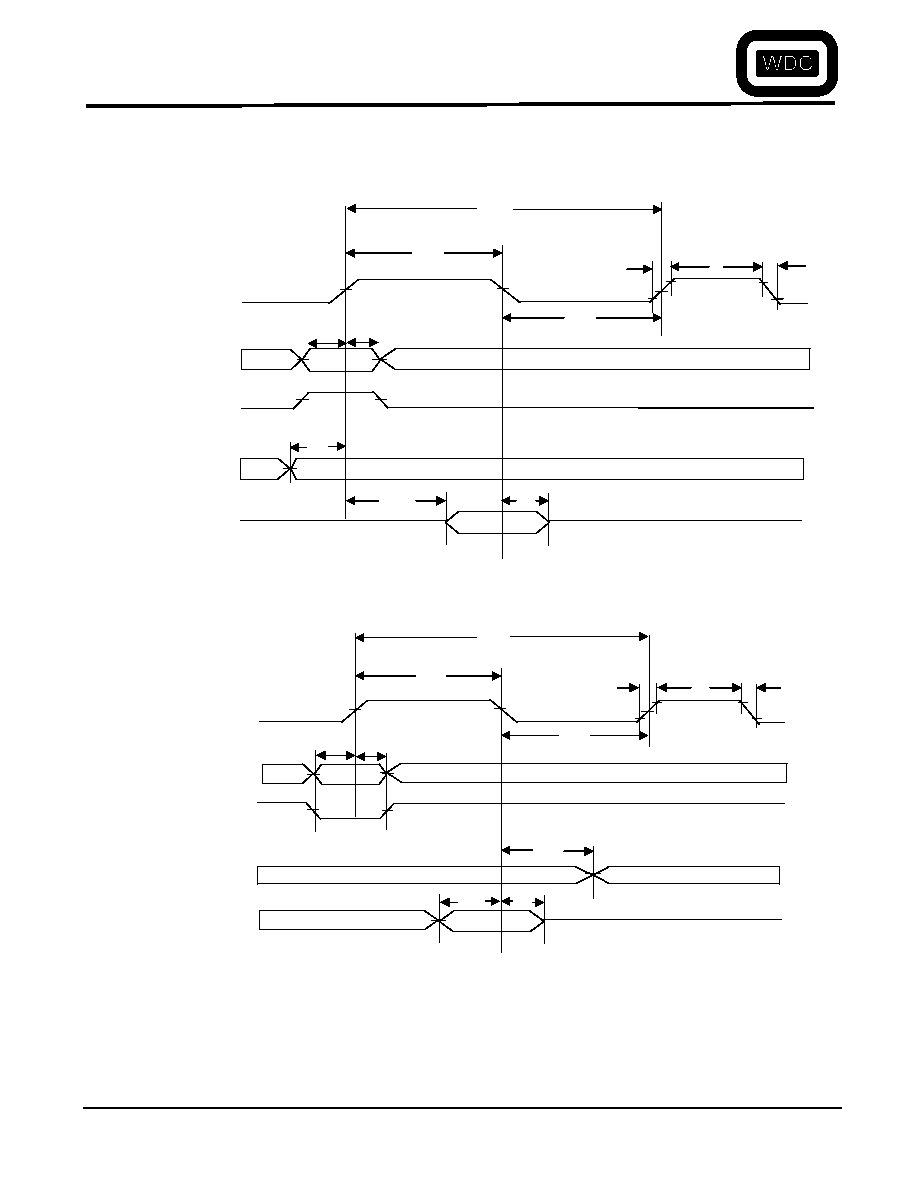
Figure 3-6 Write Handshake, Pulse Mode Timing (CA2, CB2)
Figure 3-7 Write Handshake, Handshake Mode Timing (CA2, CB2)
PHI2
WRITE, ORA, ORB
OPERATION
CA2, CB2
"DATA TAKEN"
PA, PB
PERIPHERAL DATA
tWHS
tDS
tRS3
PHI2
WRITE ORA, ORB
OPERATION
CA2, CB2
"DATA READY"
PA, PB
PERIPHERAL DATA
tDS
tRS4
ACTIVE
TRANSITION
t21
tWHS
CA1, CB1
"DATA TAKEN"

The Western Design Center, Inc.
W65C22S Data Sheet
The
Western
Design
Center
W65C22S
42
Figure 3-8 Peripheral Data, Input Latching Timing
Figure 3-9 Data Shift Out, Internal or External Shift Clock Timing
Figure 3-10 Data Shift In, Internal or External Shift Clock Timing
tSR2
PHI2
CB2
SHIFT DATA (INPUT)
CB1 SHIFT CLOCK
(iNPUT OR OUTPUT)
tSR3
SETUP TIME MEASURED FROM THE FIRST
PHI12 RISING EDGE AFTER CB1 RISING EDGE
CB1 SHIFT CLOCK
(INPUT OR OUTPUT)
CB2
SHIFT DATA (OUT0PUT)
PHI2
tSR1
DELAY TIME MEASURED FROM THE FIRST PHI2
FALLING EDGE AFTER CB1 FALLING EDGE
PA, PB
PERIPHERAL INPUT DATA
CA1, CB1
INPUT LATCHING CONTROL
T1L
tPDH
tAL
ACTIVE
TRANSITION

The Western Design Center, Inc.
W65C22S Data Sheet
The
Western
Design
Center
W65C22S
43
Figure 3-10 External Shift Clock Timing
Figure 3-11 Pulse Count Input Timing
Figure 3-12 Test Load (All Dynamic Parameters)
CB1
SHIFT CLOCK INPUT
PB6
PULSE COUNT INPUT
tICS
ACTIVE
TRANSITION
tICW
tIPW tIPS
PIN
C pF
12k
1.2k
5V

The Western Design Center, Inc.
W65C22S Data Sheet
The
Western
Design
Center
W65C22S
44
IRQB
IRQ
OLD
W65C22
IRQB
IRQ
NEW
W65C22S
RESB
RESB
4. SECTION 4 CAVEATS
4.1 Caveats
1. On older versions of the 6522 and 65C22, which are not internally chip-selected, random register are read due
to register select values. The W65C22S selects only register 15 ($F) internally. This feature has been added for
systems which have indeterminate register select values.
2. When outputting the Shift Clock, the CB1 pin may be overdriven without affecting the shifting function.
However, this is not recommended as it will result in high currents and possible damage to the part. Because
some systems have been arbitrating the clock after data has been transferred, this feature was added.
3. There is a major design difference between the W65C22S and all previous versions of the 6522 and 65C22.
The IRQB pin on the W65C22S is a standard totem pole output. It is no longer open drain and cannot be wire
OR'ed. This change was made to improve the low power, high speed characteristics of the part.
Figure 4-1 IRQB Difference
4. All W65C22S pins except PHI2 have bus holding devices. The original NMOS 6522, G65C22 and
R65C22 did not have bus holding devices.
Figure 4-2 High Resistance Bus Holding Device
5. The W65C22S output pins do not have current limiting and can over drive circuitry connected to these
pins. The original NMOS 6522 had current limiting resistors in series with PB and PA outputs.
OLD
W65C22
RESET
NEW
W65C22S
RESET
HIGH RESISTANCE
BUS HOLDING DEVICE

The Western Design Center, Inc.
W65C22S Data Sheet
The
Western
Design
Center
W65C22S
45
5. SECTION 5 HARD CORE MODEL
Application Notes
5.1
The W65C22C is functionally equivalent to the W65C22S except it does not have the output
drive transistors and does not have ESD protection.
5.2
If Chip Select, CS1 is not used, it should be held in the high state. If Chip Select, CS2B, is not used
it should be held in the low state.
5.3
The timing of the W65C22C is the same as the W65C22S in that the input buffers are the same and
the output transistor drivers are the same as the W65C22S. When applying the W65C22S core, the output
delays should be analyzed after adding the output drive transistors and the output load capacitance.

The Western Design Center, Inc.
W65C22S Data Sheet
The
Western
Design
Center
W65C22S
46
6. SECTION 6 ORDERING INFORMATION
W65C22S6TPLG-14
Description
W65C
W65C = standard product
Product Identification Number
22S
Foundry Process
6T = 0.6u TSMC Process
6T
Package
PL
P = Plastic Dual-In-Line, 40 pins
PL = Plastic Leaded Chip Carrier, 44 pins
Q = Quad Flat Pack, 44 pins
RoHS/Green Compliance
G = RoHS/Green Compliant (Wafer and Packaging)
G
Temperature/Processing
Blank = -40∫C to + 85∫C
Speed Designator
-14 = 14MHz
-14
____________________________________________________________________________________
To receive general sales or technical support on standard product or information about our module library
licenses, contact us at:
The Western Design Center, Inc.
2166 East Brown Road
Mesa, Arizona 85213 USA
Phone: 480-962-4545 Fax: 480-835-6442
e-mail: information@westerndesigncenter.com
www.westerndesigncenter.com
_______________________________________________________________________________________
WARNING: MOS CIRCUITS ARE SUBJECT TO DAMAGE FROM STATIC ELECTRICAL CHARGE
BUILDUPS. Industry established recommendations for handling MOS circuits include:
1.
Ship and store product in conductive shipping tubes or conductive foam plastic. Never ship or store
product in non-conductive plastic containers or non-conductive plastic foam material.
2.
Handle MOS parts only at conductive work stations.
3.
Ground all assembly and repair tools.