

Microcircuit, Linear,
Dual MOSFET Drivers
,
Monolithic Silicon
SIZE
A
CAGE CODE
09WF0
W98M9640
DATE:
98-09-23
REVISION LEVEL
A
SHEET
2
1.
SCOPE
1.1
Scope. This drawing describes a commercially available microcircuit with radiation tolerance.
1.1.1 **RTA** this drawing contains a radiation tolerance assured item and/or processes. All changes to items or
processes and all proposed substitutions of items identified as RTA on the drawing, must be evaluated and approved
by the Radiation Tolerance Assured Supply And Support Center (RTASSC), Directorate For Applied Technology,
Test And Simulation (DATTS), White Sands Missile Range, (WSMR).
1.1.2 Only the item described on this drawing when procured from the vendor(s) listed hereon is approved for use in
the application(s) specified hereon. A substitute item shall not be used without prior approval by the RTASSC.
1.2
Part or Identification Number (PIN). The complete part number shall be as shown in the following example.
W98 M9640
01
E
U
X
|
|
|
|
|
|
|
|
|
|
|
| |
|
|
Drawing number Device Type Device Class Case Outline Lead Finish
1.3
Drawing Number. The drawing number consists of three pieces of information as follows:
W98 = Indicates White Sands drawing, year 1998.
M = Radiation Tolerance Designator (3000 rads(Si)).
9640 = Semiconductor discrete device, P-channel power MOS field effect transistor
1.4
Device Type. The device type shall identify the circuit function as follows:
Device Type
Generic #
Circuit Function
Switchin on/off time(typ.);
Frequency(Test Condition)
01
9640
P-channel power MOSFET 57 ns / 77 ns; 1.0 MHz
1.5
Device class designator. The device class designator is a single letter identifying the product assurance level as
follows:
Device class
Device requirements documentation
E
Vendor self-certification to the requirements for MIL-STD-883 compliant,
non-JAN class level B microcircuits in accordance with MIL-PRF-38535, appendix
A
1.6
Case Outline. The case outline is as designated in MIL-STD-1835 as follows:
Outline letter Terminals
Package Style
U
4
TO-263AB, see Figure 1,
Surface Mount
1.7
Lead Finish. The lead finish is as specified in the purchase order (X indicates acceptable lead finishes per
manufacturers specification).
1.8
Operating Temperature. The operating temperature range of this device is -55
�
C to +150
�
C.

Microcircuit, Linear,
Dual MOSFET Drivers
,
Monolithic Silicon
SIZE
A
CAGE CODE
09WF0
W98M9640
DATE:
98-09-23
REVISION LEVEL
A
SHEET
3
2.0 Salient characteristics.
2.1 Maximum operating conditions. The maximum operating conditions shall be as specified in Table I.
2..2 Electrical performance characteristics:
2.2.1 The electrical performance characteristics shall be as specified in Table II.
2.2.2 The Typical characteristics diagrams shall be as specified in diagrams in Figure 2.
2.2.3 Radiation Tolerance Assurance(RTA) data for electrical performance characteristics shall be as specified in Table
III.
2.3 Design and construction. Microcircuits supplied to this WSD shall be as specified herein and on Figure 1.
2.4
Marking. Microcircuits supplied to this WSD shall be marked with the manufacturer's standard commercial PIN.
3.0 Regulatory requirements. This section is not utilized in this WSD.
TABLE I. Maximum operating conditions.
Continuous drain current I
D
, V
GS
@ 10 V,
T
C
= 25�C
T
C
= 100�C
-11 A
-6.8 A
Pulse drain current I
DM
1/
-44 A
Power dissipation P
D
@ T
C
= 25�C
(PCB Mount)
125 W
3.0 W
Linear derating factor
(PCB Mount)
1.0
W/�C
0.025 W/�C
Gate-to-Source voltage V
GS
�
20 V
Single pulse avalanche energy E
AS
2/
700 mJ
Avalanche current I
AR
1/
-11 A
Repetitive avalanche energy E
AS
1/
13 mJ
Peak diode recovery dv/dt 3/
5.0 V/ns
Operating junction temperature T
J
-55�C to +150�C
Storage temperature T
STG
-55�C to +150�C
Soldering temperature for 10 seconds
300�C (1.6mm from case)
For notes 1/, 3/ and 2/, see footnotes of TABLE II.

Microcircuit, Linear,
Dual MOSFET Drivers
,
Monolithic Silicon
SIZE
A
CAGE CODE
09WF0
W98M9640
DATE:
98-09-23
REVISION LEVEL
A
SHEET
4
TABLE II. Electrical Performance Characteristics.
Test
Symbol
Conditions
T
J
= +25�C
Group A
Limits
Units
unless otherwise specified
subgroups
Min
Typ
Max
Drain-to-source
breakdown voltage
V
(BR)DSS
V
GS
= 0 V, I
D
= 250
�
A
Room
-200
V
Breakdown voltage
temperature coefficient
V
(BR)DS
S
/
T
J
I
D
= -1 mA
-0.20
V/�C
Static drain-to-source on
resistance
R
(DS)ON
V
GS
= -10 V, I
D
= 6.6 A
4/
0.50
Gate threshold voltage
V
GS(th)
V
DS
= V
GS
, I
D
= 250
�
A
-2.0
-4.0
V
Forward
transconductance
g
fs
V
DS
= -50 V, I
D
= 6.6 A
4/
4.1
S
Drain-to-source leakage
I
DSS
V
DS
= -200 V, V
GS
= 0 V
-100
�
A
current
V
DS
= -160 V, V
GS
= 0 V
Max.
-500
Gate-to-source forward
leakage current
I
GSS
V
GS
= -20 V
Room
-100
nA
Gate-to-source reverse
leakage current
V
GS
= 20 V
100
Total gate charge
Q
g
I
D
= -11 A
44
nC
Gate-to-source charge
Q
gs
V
DS
= -160 V
7.1
Gate-to-drain (Miller)
charge
Q
gd
V
GS
= -10 V (see Figures 3.6 and
3.13) 4/
27
Turn-on delay time
t
d(ON)
V
DD
= -100 V
14
ns
Rise time
t
r
I
D
= -11 A
43
Turn-off delay time
t
d(off)
R
G
= 9.1
39
Fall time
t
f
R
G
= 8.6
(see Figure 2.10) 4/
38
Internal drain inductance
L
D
Between lead, 6 mm (0.25in) from
4.5
nH
Internal source
inductance
L
S
package and center of die contact
5A/
7.5
Input capacitance
C
ISS
V
GS
= 0 V
1200
pF
Output capacitance
C
OSS
V
DS
= -25 V
370
Reverse transfer
capacitance
C
rSS
f = 1.0 MHz (see Figure 2.5)
81
See footnotes at end of table.

Microcircuit, Linear,
Dual MOSFET Drivers
,
Monolithic Silicon
SIZE
A
CAGE CODE
09WF0
W98M9640
DATE:
98-09-23
REVISION LEVEL
A
SHEET
5
TABLE II. Electrical performance characteristics- Continued.
Test
Symbol
Conditions
T
J
= +25�C
Group A
Limits
Units
unless otherwise specified
subgroups
Min
Typ
Max
Source-Drain Ratings :
Continuous source
current (body diode)
I
S
MOSFET symbol showing the
integral reverse p-n junction diode
5B/
Room
-11
A
Pulsed source current
(body diode)
I
SM
-44
Diode forward voltage
V
SD
I
S
= -11 A, V
GS
= 0 V
4/
-5.0
V
Reverse recovery time
t
rr
I
F
= -11 A, di/dt = 100 A/
�
s 4/
250
300
ns
Reverse recovery charge
Q
rr
2.9
3.6
�
C
Forward turn-on time
t
on
turn-on is dominated by L
S
+ L
D
intrinsic turn-on is neglible
1/ Repetitive rating; pulse width limited by max. Junction temperature (see Figure 2.11)
2/ VDD = -50 V, starting TJ = +25�C, L = 8.7 mH, RG = 25
, IAS = -11 A (see Figure 2.12).
3/ I
SD
-11 A, di/dt
150 A/
�
s, V
DD
V
(BR)DSS
, T
J
+150�C.
4/ Pulse width
300
�
s; duty cycle
2%.
Insert A.
Insert B.

Microcircuit, Linear,
Dual MOSFET Drivers
,
Monolithic Silicon
SIZE
A
CAGE CODE
09WF0
W98M9640
DATE:
98-09-23
REVISION LEVEL
A
SHEET
6
Terminal connections
Package Outline
Figure 1. Design and construction.
Microcircuit, Linear,
Dual MOSFET Drivers
,
Monolithic Silicon
SIZE
A
CAGE CODE
09WF0
W98M9640
DATE:
98-09-23
REVISION LEVEL
A
SHEET
7
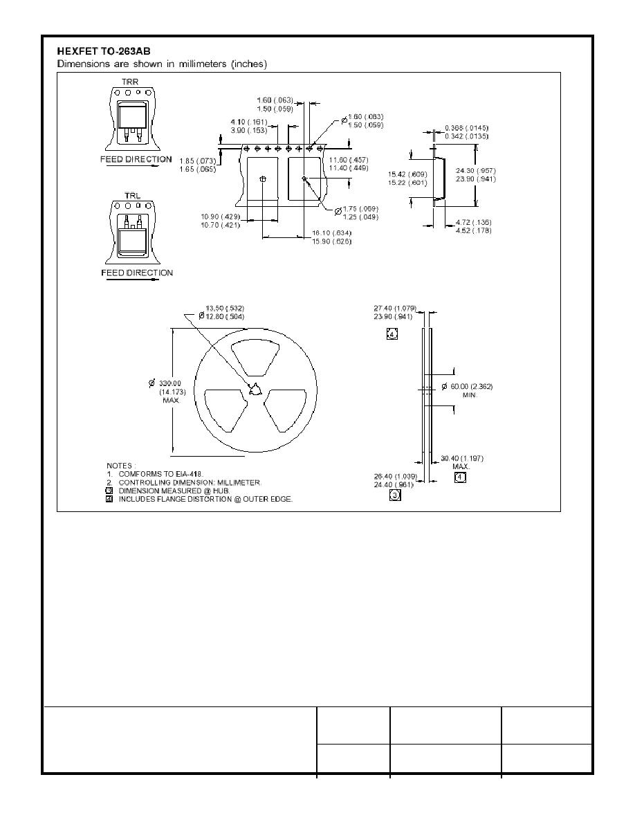
Tape & Reel Information
Figure 1. Design and construction- Continued.

Microcircuit, Linear,
Dual MOSFET Drivers
,
Monolithic Silicon
SIZE
A
CAGE CODE
09WF0
W98M9640
DATE:
98-09-23
REVISION LEVEL
A
SHEET
8
Figure 2.
Typical characteristics diagrams.

Microcircuit, Linear,
Dual MOSFET Drivers
,
Monolithic Silicon
SIZE
A
CAGE CODE
09WF0
W98M9640
DATE:
98-09-23
REVISION LEVEL
A
SHEET
9
Figure 2.
Typical characteristics diagrams - Continued.

Microcircuit, Linear,
Dual MOSFET Drivers
,
Monolithic Silicon
SIZE
A
CAGE CODE
09WF0
W98M9640
DATE:
98-09-23
REVISION LEVEL
A
SHEET
10
Figure 2.
Typical characteristics diagrams - Continued.

Microcircuit, Linear,
Dual MOSFET Drivers
,
Monolithic Silicon
SIZE
A
CAGE CODE
09WF0
W98M9640
DATE:
98-09-23
REVISION LEVEL
A
SHEET
11
4.0 Quality assurance provisions.
4.1 Responsibility for inspection. Unless otherwise specified in the contract or purchase order, the contractor is responsible for the
performance of all inspection, examination, and test requirements specified herein. Except as otherwise specified in the contract
or purchase order, the contractor may use his own or any other facilities suitable for the inspection requirements specified herein,
unless disapproved by the Government. The Government reserves the right to perform any of the inspections, examinations, or
tests set forth in this description where such inspections, examinations, and tests are deemed necessary to assure supplies and
services conform to prescribed requirements.
4.2 Contractor certification statement. The contractor shall certify and maintain objective quality evidence that the product offered
meets the requirements of this WSD, and that the product conforms to the producer's own drawings, specifications, standards,
quality assurances practices, and is the same as the product provided as a bid sample. The acquiring activity reserves the right to
require proof of such conformance prior to the first delivery and thereafter as may be otherwise provided for under the provisions
of the contract.
4.3 Certificate of conformance. A certificate of conformance shall accompany all microcircuits supplied to this WSD.
5.1 Preservation, packaging, packing, labeling, and marking. Preservation, packaging, labeling, and marking shall be as specified in
the contract or purchase order.
6.0 Notes. This section contains relevant information which is useful to buyers, users, and suppliers in the process of acquiring the
item, but is not mandatory.
6.1
Radiation Tolerance Assured (RTA) . RTA performance is not covered under the manufacturers warranty. RTA testing has been
performed and is an integral part of this drawing. The RTA performance is certified by White Sands Missile Range, Directorate
for Applied Technology, Test and Simulation (WSMR, DATTS) to the performance characteristics as specified in TABLE III
herein.
6.2 Electrical Performance over Temperature . Electrical performance over temperature ( -55�C
T
A
+150�C) is covered
under the manufacturers warranty. No further temperature testing is required for determining temperature related effects.
There is no certification or warrantees by WSMR,DATTS to the performance characteristics specified in TABLE II herein.

Microcircuit, Linear,
Dual MOSFET Drivers
,
Monolithic Silicon
SIZE
A
CAGE CODE
09WF0
W98M9640
DATE:
98-09-23
REVISION LEVEL
A
SHEET
12
TABLE III. RTA Electrical Performance Characteristics.
1/
Test
Symbol
Conditions 2/
T
J
= +25�C
Limits
Units
unless otherwise specified
Min
Max
Drain-to-source breakdown voltage
V
(BR)DSS
V
GS
= 0 V, I
D
= 250
�
A
-200
V
Static drain-to-source on resistance
R
(DS)ON
V
GS
= -10 V, I
D
= 6.6 A
0.6
Gate threshold voltage
V
GS(th)
V
DS
= V
GS
, I
D
= 250
�
A
-2.0
-4.4
V
Forward transconductance
g
fs
V
DS
= -9 V, I
D
= 6.6 A
3.9
S
Drain-to-source leakage current
I
DSS
V
DS
= -200 V, V
GS
= 0 V
-133
�
A
Gate-to-source forward leakage current
I
GSS
V
GS
= -20 V
-110
nA
Gate-to-source reverse leakage current
V
GS
= 20 V
110
Diode forward voltage
V
SD
I
S
= -11 A, V
GS
= 0 V
-5.2
V
1/ Devices supplied to this drawing will meet and only be tested at the level M of irradiation. When performing post irradiation
electrical measurements for any radiation level, T
A
= +25�C.
Radiation measurements at the level M are performed for:
Gamma total dose . . . . . . . . . . . . . . . . . . . . . . . . . . . . . . . . . . . 3000 Rads(Si)
Neutron fluence . . . . . . . . . . . . . . . . . . . . . . . . . . . . . . . . 2.5x10
12
n/cm
2
/Mev
2/ All footnotes of Table II shall be applied here unless otherwise specified.

6.3 Ordering data. The contract or purchase order shall specify the following:
a. WSD document number and revision and WSD PIN.
b. Quality assurance provisions.
c. Packaging requirements.
6.4 Identification of the approved source(s) of supply hereon is not to be construed as a guarantee of present or continued availability as a
source of supply for the item described on the drawing.
PART ID NUMBER
CAGE CODE
MANUFACTURER
ITEM IDENTIFICATION
W98M964001EUX
09WF0
International Rectifier
IRF9640S
09WF0 Commander, USAWSMR
ATTN: STEWS-DT-A
Building 90121
White Sands NM 88002-5158
Semiconductor Discrete Device, P-
Channel Power MOS Field Effect
SIZE
A
CAGE CODE
09WF0
W98M9640
Transistor
DATE:
98-09-25
REVISION LEVEL
A
SHEET
13