
1
White Microelectronics ∑ Phoenix, AZ ∑ (602) 437-1520
4
SRAM MODULES
WS512K32BV-XXXE
512Kx32 3.3V SRAM MODULE
PRELIMINARY*
s Commercial, Industrial and Military Temperature Ranges
s 3.3 Volt Power Supply
s BiCMOS
s TTL Compatible Inputs and Outputs
s Built-in Decoupling Caps and Multiple Ground Pins for Low
Noise Operation
s Weight
WS512K32BV-XG2XE - 8 grams typical
WS512K32NBV-XH2XE - 13 grams typical
* This data sheet describes a product under development, not fully
characterized, and is subject to change without notice.
This speed is Advanced information.
FEATURES
s Access Times of 15
, 17, 20ns
s MIL-STD-883 Compliant Devices Available
s Low Voltage Operation
s Packaging
∑ 66-pin, PGA Type, 1.385 inch square Hermetic Ceramic HIP
(Package 402)
∑ 68 lead, Hermetic CQFP (G2), 22mm (0.880 inch) square
(Package 500). Designed to fit JEDEC 68 lead 0.990" CQFJ
footprint
s Organized as 512Kx32; User Configurable as 1Mx16 or 2Mx8
s Radiation Tolerant with Epitaxial Layer Die
PIN CONFIGURATION FOR WS512K32NBV-XH2XE
PIN DESCRIPTION
I/O
0-31
Data Inputs/Outputs
A
0-18
Address Inputs
WE
1-4
Write Enables
CS
1-4
Chip Selects
OE
Output Enable
V
CC
Power Supply
GND
Ground
NC
Not Connected
I/O
8
I/O
9
I/O
10
A
13
A
14
A
15
A
16
A
17
I/O
0
I/O
1
I/O
2
WE
2
CS
2
GND
I/O
11
A
10
A
11
A
12
V
CC
CS
1
NC
I/O
3
I/O
15
I/O
14
I/O
13
I/O
12
OE
A
18
WE
1
I/O
7
I/O
6
I/O
5
I/O
4
I/O
24
I/O
25
I/O
26
A
6
A
7
NC
A
8
A
9
I/O
16
I/O
17
I/O
18
V
CC
CS
4
WE
4
I/O
27
A
3
A
4
A
5
WE
3
CS
3
GND
I/O
19
I/O
31
I/O
30
I/O
29
I/O
28
A
0
A
1
A
2
I/O
23
I/O
22
I/O
21
I/O
20
11 22 33 44 55 66
1 12 23 34 45 56
TOP VIEW
BLOCK DIAGRAM
512K x 8
8
I / O
0 - 7
CS
1
512K x 8
8
I / O
8 - 1 5
2
512K x 8
8
I / O
1 6 - 2 3
3
512K x 8
8
I / O
2 4 - 3 1
4
A
0 - 1 8
O E
WE
CS
WE
CS
WE
CS
WE
1
2
3
4
February 1998

2
White Microelectronics ∑ Phoenix, AZ ∑ (602) 437-1520
4
SRAM MODULES
WS512K32BV-XXXE
PIN DESCRIPTION
I/O
0-31
Data Inputs/Outputs
A
0-18
Address Inputs
WE
1-4
Write Enables
CS
1-4
Chip Selects
OE
Output Enable
Vcc
Power Supply
GND
Ground
NC
Not Connected
512K x 8
8
I / O
0 - 7
CS
1
512K x 8
8
I / O
8 - 1 5
2
512K x 8
8
I / O
1 6 - 2 3
3
512K x 8
8
I / O
2 4 - 3 1
4
A
0 - 1 8
O E
WE
CS
WE
CS
WE
CS
WE
1
2
3
4
BLOCK DIAGRAM
10
11
12
13
14
15
16
17
18
19
20
21
22
23
24
25
26
60
59
58
57
56
55
54
53
52
51
50
49
48
47
46
45
44
9 8 7 6 5 4 3 2 1 68 67 66 65 64 63 62 61
27 28 29 30 31 32 33 34 35 36 37 38 39 40 41 42 43
I/O
0
I/O
1
I/O
2
I/O
3
I/O
4
I/O
5
I/O
6
I/O
7
GND
I/O
8
I/O
9
I/O
10
I/O
11
I/O
12
I/O
13
I/O
14
I/O
15
V
CC
A
11
A
12
A
13
A
14
A
15
A
16
CS
1
OE
CS
2
A
17
WE
2
WE
3
WE
4
A
18
NC
NC
I/O
16
I/O
17
I/O
18
I/O
19
I/O
20
I/O
21
I/O
22
I/O
23
GND
I/O
24
I/O
25
I/O
26
I/O
27
I/O
28
I/O
29
I/O
30
I/O
31
NC
A
0
A
1
A
2
A
3
A
4
A
5
CS
3
GND
CS
4
WE
1
A
6
A
7
A
8
A
9
A
10
V
CC
TOP VIEW
The White 68 lead G2 CQFP fills
the same fit and function as the
JEDEC 68 lead CQFJ or 68 PLCC.
But the G2 has the TCE and lead
inspection advantage of the
CQFP form.
0.940"
PIN CONFIGURATION FOR WS512K32BV-XG2XE
3
White Microelectronics ∑ Phoenix, AZ ∑ (602) 437-1520
4
SRAM MODULES
WS512K32BV-XXXE
CAPACITANCE
(T
A
= +25
∞
C)
Parameter
Symbol
Conditions
Max
Unit
OE capacitance
C
OE
V
IN
= 0 V, f = 1.0 MHz
50
pF
WE
1-4
capacitance
C
WE
V
IN
= 0 V, f = 1.0 MHz
pF
HIP (PGA)
20
CQFP G2
20
CS
1-4
capacitance
C
CS
V
IN
= 0 V, f = 1.0 MHz
20
pF
Data I/O capacitance
C
I/O
V
I/O
= 0 V, f = 1.0 MHz
20
pF
Address input capacitance
C
AD
V
IN
= 0 V, f = 1.0 MHz
50
pF
This parameter is guaranteed by design but not tested.
TRUTH TABLE
ABSOLUTE MAXIMUM RATINGS
Parameter
Symbol
Min
Max
Unit
Operating Temperature
T
A
-55
+125
∞
C
Storage Temperature
T
STG
-65
+150
∞
C
Signal Voltage Relative to GND
V
G
-0.5
4.6
V
Junction Temperature
T
J
150
∞
C
Supply Voltage
V
CC
-0.5
4.6
V
CS
OE
WE
Mode
Data I/O
Power
H
X
X
Standby
High Z
Standby
L
L
H
Read
Data Out
Active
L
X
L
Write
Data In
Active
L
H
H
Out Disable
High Z
Active
RECOMMENDED OPERATING CONDITIONS
Parameter
Symbol
Min
Max
Unit
Supply Voltage
V
CC
3.0
3.6
V
Input High Voltage
V
IH
2.2
V
CC
+ 0.3
V
Input Low Voltage
V
IL
-0.3
+0.8
V
DC CHARACTERISTICS
(V
CC
= 3.3V
±
0.3V, V
SS
= 0V, T
A
= -55
∞
C to +125
∞
C)
Parameter
Sym
Conditions
Units
Min
Max
Input Leakage Current
I
LI
V
IN
= GND to V
CC
10
µ
A
Output Leakage Current
I
LO
CS = V
IH
, OE = V
IH
, V
OUT
= GND to V
CC
10
µ
A
Operating Supply Current (x 32 Mode)
I
CC
x 32
CS = V
IL
, OE = V
IH
, f = 5MHz, V
CC
= 3.6V
480
mA
Standby Current
I
SB
CS = V
IH
, OE = V
IH
, f = 5MHz, V
CC
= 3.6V
110
mA
Output Low Voltage
V
OL
I
OL
= 8mA
0.4
V
Output High Voltage
V
OH
I
OH
= -4.0mA
2.4
V
NOTE: DC test conditions: V
IH
= V
CC
-0.3V, V
IL
= 0.3V
4
White Microelectronics ∑ Phoenix, AZ ∑ (602) 437-1520
4
SRAM MODULES
WS512K32BV-XXXE
AC TEST CIRCUIT
NOTES:
V
Z
is programmable from -2V to +7V.
I
OL
& I
OH
programmable from 0 to 16mA.
Tester Impedance Z
0
= 75
.
V
Z
is typically the midpoint of V
OH
and V
OL
.
I
OL
& I
OH
are adjusted to simulate a typical resistive load circuit.
ATE tester includes jig capacitance.
I
Current Source
D.U.T.
C = 50 pf
eff
I
OL
V
1.5V
(Bipolar Supply)
Z
Current Source
OH
AC TEST CONDITIONS
Parameter
Typ
Unit
Input Pulse Levels
V
IL
= 0, V
IH
= 2.5
V
Input Rise and Fall
5
ns
Input and Output Reference Level
1.5
V
Output Timing Reference Level
1.5
V
AC CHARACTERISTICS
(V
CC
= 3.3V, T
A
= -55
∞
C to +125
∞
C)
Parameter
Symbol
-15*
-17
-20
Units
Read Cycle
Min
Max
Min
Max
Min
Max
Read Cycle Time
t
RC
15
17
20
ns
Address Access Time
t
AA
15
17
20
ns
Output Hold from Address Change
t
OH
0
0
0
ns
Chip Select Access Time
t
ACS
15
17
20
ns
Output Enable to Output Valid
t
OE
7
8
10
ns
Chip Select to Output in Low Z
t
CLZ
1
2
2
2
ns
Output Enable to Output in Low Z
t
OLZ
1
0
0
0
ns
Chip Disable to Output in High Z
t
CHZ
1
7
8
10
ns
Output Disable to Output in High Z
t
OHZ
1
7
8
10
ns
1. This parameter is guaranteed by design but not tested.
* Advanced information.
AC CHARACTERISTICS
(V
CC
= 3.3V, T
A
= -55
∞
C to +125
∞
C)
Parameter
Symbol
-15*
-17
-20
Units
Write Cycle
Min
Max
Min
Max
Min
Max
Write Cycle Time
t
WC
15
17
20
ns
Chip Select to End of Write
t
CW
10
12
14
ns
Address Valid to End of Write
t
AW
10
12
14
ns
Data Valid to End of Write
t
DW
8
9
10
ns
Write Pulse Width
t
WP
12
14
14
ns
Address Setup Time
t
AS
0
0
0
ns
Address Hold Time
t
AH
0
0
0
ns
Output Active from End of Write
t
OW
1
2
3
3
ns
Write Enable to Output in High Z
t
WHZ
1
8
8
9
ns
Data Hold Time
t
DH
0
0
0
ns
1. This parameter is guaranteed by design but not tested.
* Advanced information.

5
White Microelectronics ∑ Phoenix, AZ ∑ (602) 437-1520
4
SRAM MODULES
WS512K32BV-XXXE
WS32K32-XHX
TIMING WAVEFORM - READ CYCLE
WRITE CYCLE - CS CONTROLLED
WRITE CYCLE - WE CONTROLLED
ADDRESS
DATA I/O
WRITE CYCLE 1, WE CONTROLLED
t
AW
t
CW
t
AH
t
WP
t
DW
t
WHZ
t
AS
t
OW
t
DH
t
WC
DATA VALID
CS
WE
ADDRESS
DATA I/O
WRITE CYCLE 2, CS CONTROLLED
t
AW
t
AS
t
CW
t
AH
t
WP
t
DH
t
DW
t
WC
CS
WE
DATA VALID
ADDRESS
DATA I/O
READ CYCLE 2 (WE = V
IH
)
t
AA
t
ACS
t
OE
t
CLZ
t
OLZ
t
OHZ
t
RC
DATA VALID
HIGH IMPEDANCE
CS
OE
t
CHZ
ADDRESS
DATA I/O
READ CYCLE 1 (CS = OE = V
IL
, WE = V
IH
)
t
AA
t
OH
t
RC
DATA VALID
PREVIOUS DATA VALID
6
White Microelectronics ∑ Phoenix, AZ ∑ (602) 437-1520
4
SRAM MODULES
WS512K32BV-XXXE
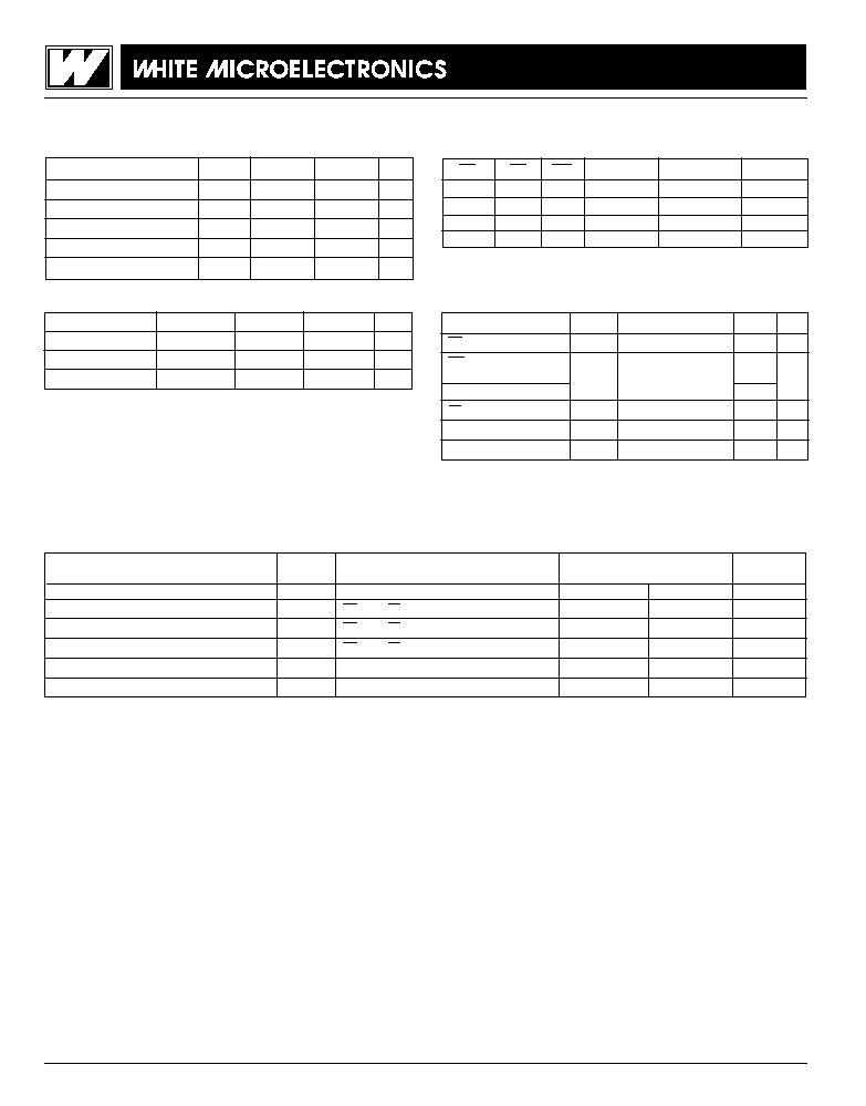
PACKAGE 402:
66 PIN, PGA TYPE, CERAMIC HEX-IN-LINE PACKAGE, HIP (H2)
35.2 (1.385)
±
0.38 (0.015) SQ
25.4 (1.0) TYP
15.24 (0.600) TYP
0.76 (0.030)
±
0.1 (0.005)
5.7 (0.223)
MAX
3.81 (0.150)
±
0.1 (0.005)
2.54 (0.100)
TYP
25.4 (1.0) TYP
1.27 (0.050)
±
0.1 (0.005)
1.27 (0.050) TYP DIA
0.46 (0.018)
±
0.05 (0.002) DIA
PIN 1 IDENTIFIER
SQUARE PAD
ON BOTTOM
ALL LINEAR DIMENSIONS ARE MILLIMETERS AND PARENTHETICALLY IN INCHES
7
White Microelectronics ∑ Phoenix, AZ ∑ (602) 437-1520
4
SRAM MODULES
WS512K32BV-XXXE
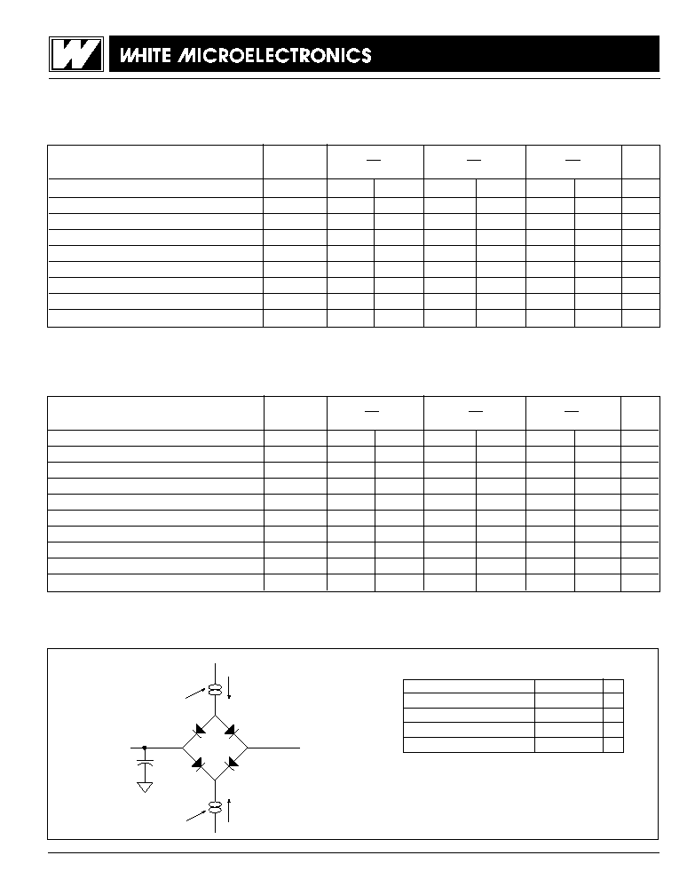
PACKAGE 500:
68 LEAD, CERAMIC QUAD FLAT PACK, CQFP (G2)
0.38 (0.015)
±
0.05 (0.002)
0.25 (0.010)
±
0.1 (0.002)
25.1 (0.990)
±
0.25 (0.010) SQ
1.27 (0.050) TYP
24.0 (0.946)
±
0.25 (0.010)
22.4 (0.880)
±
0.25 (0.010) SQ
20.3 (0.800) REF
5.1 (0.200) MAX
0.25 (0.010)
±
0.127 (0.005)
23.87
(0.940) REF
1.0 (0.040)
±
0.127 (0.005)
0.25 (0.010) REF
1
∞
/ 7
∞
R 0.25
(0.010)
DETAIL A
SEE DETAIL "A"
Pin 1
ALL LINEAR DIMENSIONS ARE MILLIMETERS AND PARENTHETICALLY IN INCHES
The White 68 lead G2 CQFP fills
the same fit and function as the
JEDEC 68 lead CQFJ or 68 PLCC.
But the G2 has the TCE and lead
inspection advantage of the
CQFP form.
0.940"
TYP

8
White Microelectronics ∑ Phoenix, AZ ∑ (602) 437-1520
4
SRAM MODULES
WS512K32BV-XXXE
ORDERING INFORMATION
LEAD FINISH:
Blank = Gold plated leads
A = Solder dip leads
E = Epitaxial Layer
DEVICE GRADE:
M = Military Screened
-55
∞
C to +125
∞
C
I = Industrial
-40
∞
C to +85
∞
C
C = Commercial
0
∞
C to +70
∞
C
PACKAGE TYPE:
H2 = Ceramic Hex-In-line Package, HIP (Package 402)
G2 = 22 mm Ceramic Quad Flat Pack, CQFP (Package 500)
ACCESS TIME (ns)
Low Voltage Supply 3.3V
±
10%
BiCMOS
IMPROVEMENT MARK:
N = No Connect at pin 21 and 39 in HIP for Upgrades
ORGANIZATION, 512Kx32
User configurable as 1Mx16 or 2Mx8
SRAM
WHITE MICROELECTRONICS
W S 512K 32 X B V - XXX X X E X