YOUDA INTEGRATED CIRCUIT
YD324
FOUR OPERATIONAL AMPLIFIER-YD324
DESCRIPTION AND FEATURES
These devices consist of four independent high-gain, phase ≠compensated operational amplifiers. A suitable
recorder and Audio System for tone control. Can also used for telecom and instrument.
*Built-in phase-compensated circuit
*Operating supply voltage range : V
CC
=3.030.0V or V
CC
=±1.5±15V
*Input voltage can low to 0V
*Output voltage range :0VV
CC
-1.5V
*Supply current : I
CC
=0.6mA (R
L
=)
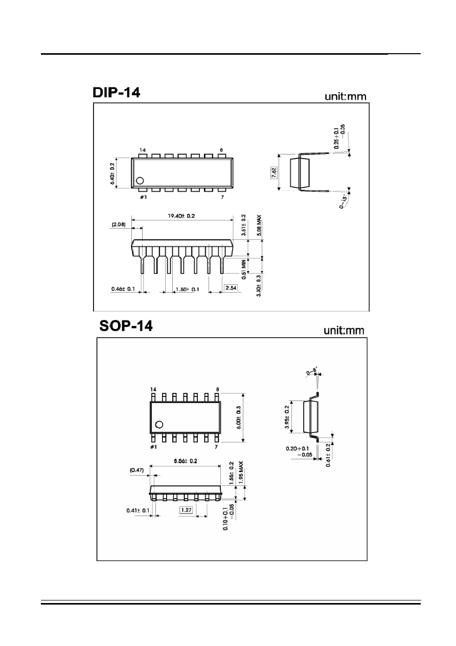
*DIP14 and SOP14
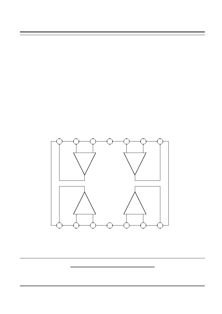
BLOCK DIAGRAM
1
2
3
4
5
6
7
8
9
10
11
12
13
14
-
+
Amp4
+
-
Amp3
-
+
Amp1
+
-
Amp2
GND
Vcc
WuXi YouDa Electronics Co., Ltd
Add: No.5 Xijin Road, National Hi-Tech Industrial Development Zone, Wuxi Jiangsu China
Tel: 86-510-5205117 86-510-5205106 Fax: 86-510-5205110 Website: www.e-youda.com
SHENZHEN OFFICE Tel 86-755-83740369 Fax 86-755-83741418
Ver 5.0 1 of 4 2006-08-08
YOUDA INTEGRATED CIRCUIT
YD324
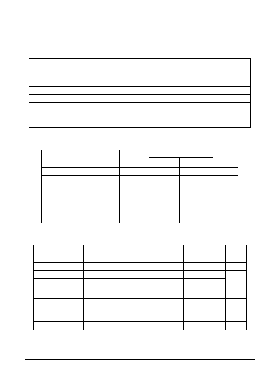
PIN DESCRIPTION
PIN
NO.
CONTENT SYMBOL
PIN
NO.
CONTENT SYMBOL
1
Output of CH1
OUT
1
8
Output of CH3
OUT
3
2
Inverting Input of CH1
1N-(1)
9
Inverting Input of CH3
1N-(3)
3
Non-inverting Input of CH1
1N+(1)
10
Non-inverting Input of CH3
1N+(3)
4
Supply Voltage
V
CC
11
Ground GND
5
Non-inverting Input of CH2
1N+(2)
12
Non-inverting Input of CH4
1N+(4)
6
Inverting Input of CH2
1N-(2)
13
Inverting Input of CH4
1N-(4)
7
Output of CH2
OUT
2
14
Output of CH4
OUT
4
ABSOLUTE MAXIMUM RATINGS
VALUE
PARAMETER
SYMBOL
MIN MAX
UNIT
Supply Voltage
V
CC
32 V
Differential Input Voltage
V
ID
32 V
Input Voltage
V
I
-0.3 32 V
Total Dissipation(DIP14)
P
D1
720
mW
Total Dissipation(SOP14)
P
D2
300
mW
Operating Temperature Range
Topr
-30
85
Storage Temperature Range
Tstg
-55
125
ELECTRICAL CHARACTERISTICS
(Tamb=25, V
CC
=9V, Unless otherwise specified)
PARAMETER SYMBOL
TEST
CONDITION
MIN TYP
MAX
UNIT
Input Offset Voltage
V
IO
±
2
±
7
mv
Input Offset Current
I
IO
±
5
±
50
Input Bias Current
I
IB
45
250
nA
Common-mode Input
Voltage Range
V
ICM
0
V
CC
-1.5 V
Common-mode
Rejection Ratio
K
CmR
65
80
Open Loop Voltage
Gain
A
VO
V
CC
=15V, R
L
2k
88 100
dB
Output Voltage Range
V
O
0
V
CC
-1.5 V
WuXi YouDa Electronics Co., Ltd 2 of 4 Website: www.e-youda.com
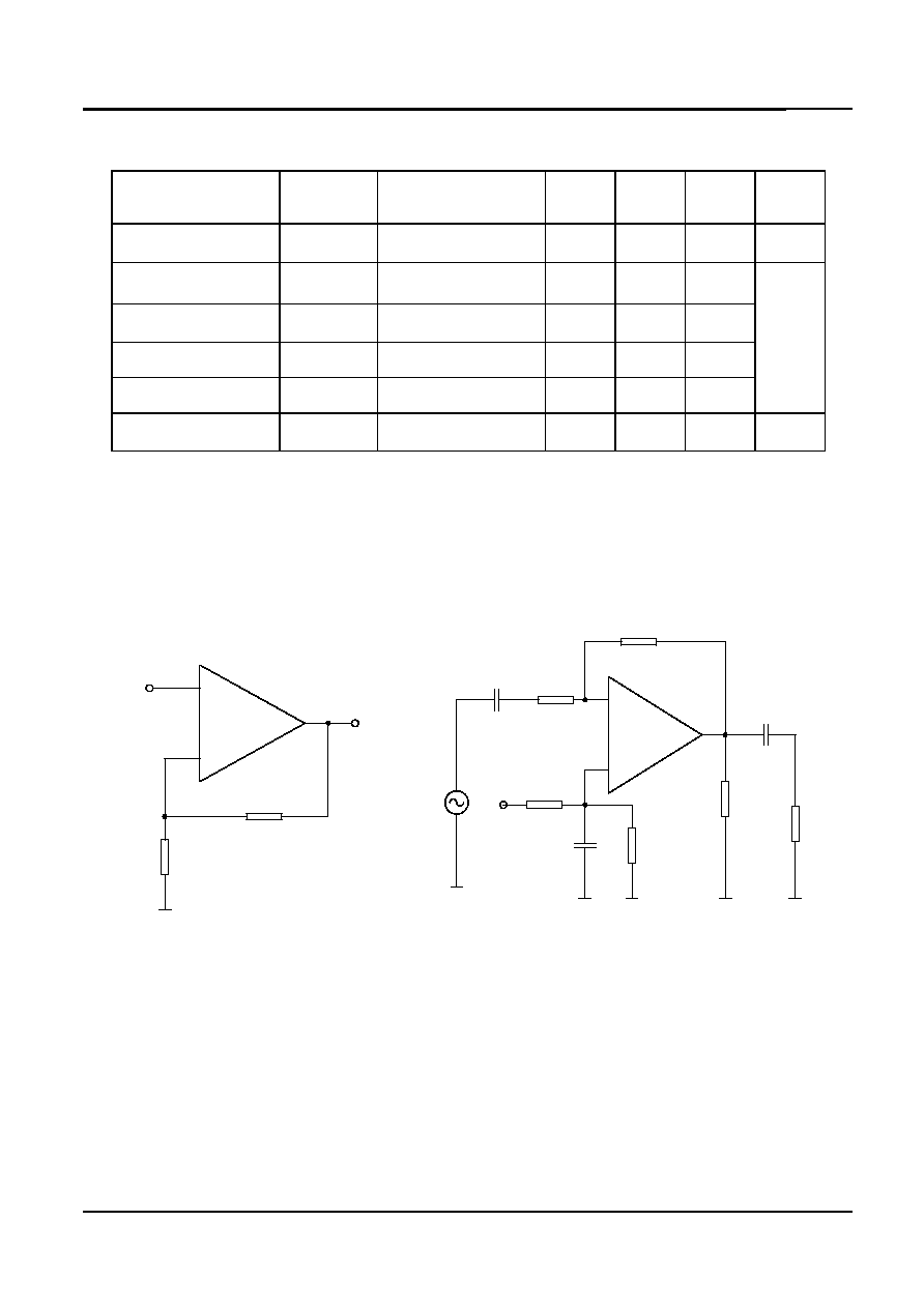
YOUDA INTEGRATED CIRCUIT
YD324
PARAMETER SYMBOL
TEST
CONDITION
MIN TYP
MAX
UNIT
Supply Voltage
Rejection Ratio
K
SVR
65
100
dB
Output Current
I
OS
20
40
Output Current Of
Sink
Iosink 10
20
Supply Current
I
CCQ
0.6
2
Supply Current
I
CCQ
V
CC
=30V
1.5
3
mA
Channel Separation
C
S
f=1k20kHz
120 dB
APPLICATION CIRCUIT
DC AMPLIFICATION AC AMPLIFICATION
R2
1M
R1
10k
+
-
+Vin
AMP.
+Vo
-
+
R1
10k
R4
100k
R5
6.2k
C1
10F
R2
100k
R3
100k
Co
R6
10k
Cin
Vin
+
Av=1+R2/R1
Av=R4/R1
Vcc
AMP.
WuXi YouDa Electronics Co., Ltd 3 of 4 Website: www.e-youda.com