
Mar. 2002
1
ZC0301
VGA & CIF USB PC Camera Controller
ZC0301
VGA USB PC Camera Controller
Vimicro Corporation
Preliminary
Data Sheet
Vimicro Corporation reserves the right to make changes without further notice to any product herein to improve reliability,
function or design. Vimicro does not assume any liability arising out of the application or use of any project, circuit described
herein; neither does it convey any license under its patent nor the right of others.
This document contains information of a proprietary nature. None of this information shall be divulged to persons other than
Vimicro Microelectronics Corporation employee authorized by the nature of their duties to receive such information, or
individuals or organizations authorized by Vimicro Corporation.

Mar. 2002
2
ZC0301
VGA & CIF USB PC Camera Controller
Contents
1.
Features.................................................................................................. 4
2.
Architecture ........................................................................................... 5
2.1.
System Controller.................................................................................................................. 5
2.2.
Image Signal Processor......................................................................................................... 5
2.3.
Sub-Sample & Raster ........................................................................................................... 5
2.4.
JPEG Encoder ....................................................................................................................... 6
2.5.
USB Device Controller.......................................................................................................... 6
3.
Pin Definition......................................................................................... 7
3.1.
Pin Assignment...................................................................................................................... 7
3.2.
Pin Description ...................................................................................................................... 7
4.
Electrical Characteristics...................................................................... 9
4.1.
Absolute Maximum Ratings................................................................................................. 9
4.2.
DC Characteristics ................................................................................................................ 9
4.3.
USB Transceiver AC Characteristics .................................................................................. 9
4.4.
RESET Timing AC Characteristics................................................................................... 10
4.5.
Clock AC Characteristics ................................................................................................... 10
4.6.
Input Signal AC Characteristics........................................................................................ 11
5.
Register Table (Vendor Commands)...................................................11
6.
Mechanical Information ..................................................................... 12
Appendix I Sensor Interface Description ................................................ 13

Mar. 2002
3
ZC0301
VGA & CIF USB PC Camera Controller
Illustrations
F
IGURE
1 USB PC C
AMERA
S
YSTEM
B
LOCK
D
IAGRAM
.......................................................4
F
IGURE
2 ZC0301 F
UNCTIONAL
B
LOCK
D
IAGRAM
..............................................................5
F
IGURE
3 28-P
IN
PLCC P
ACKAGE
........................................................................................7
F
IGURE
4 RESET T
IMING
AC C
HARACTERISTICS
D
IAGRAM
............................................ 10
F
IGURE
5 C
LOCK
T
IMING
AC C
HARACTERISTICS
D
IAGRAM
............................................. 10
F
IGURE
6 I
NPUT
S
IGNAL
T
IMING
AC C
HARACTERISTICS
D
IAGRAMS
................................ 11
F
IGURE
7 28-P
IN
PLCC P
ACKAGE
D
IAGRAM
.................................................................... 12
Tables
T
ABLE
1 S
ENSOR
I
NTERFACE
(15 P
INS
) ................................................................................7
T
ABLE
2 USB H
OST
I
NTERFACE
(2 P
INS
).............................................................................8
T
ABLE
3 C
LOCK
, R
ESET
,
AND
M
ISCELLANEOUS
(5 P
INS
).....................................................8
T
ABLE
4 P
OWER AND
G
ROUND
(6 P
INS
)...............................................................................8
T
ABLE
5 M
AXIMUM
R
ATINGS
...............................................................................................9
T
ABLE
6 DC C
HARACTERISTICS
..........................................................................................9
T
ABLE
7 F
ULL
-S
PEED
D
RIVER
E
LECTRICAL
C
HARACTERISTICS
...........................................9
T
ABLE
8 L
OW
-S
PEED
D
RIVER
E
LECTRICAL
C
HARACTERISTICS
............................................9
T
ABLE
9
R
ESET
S
IGNAL
AC C
HARACTERISTICS
................................................................ 10
T
ABLE
10 C
LOCK
S
IGNAL
AC C
HARACTERISTICS
............................................................. 10
T
ABLE
11 I
NPUT
S
IGNAL
AC C
HARACTERISTICS
............................................................... 11
T
ABLE
12 S
YSTEM
C
ONTROL
R
EGISTER
............................................................................ 11
T
ABLE
13 ZC0301 P
ACKAGE
D
IMENSION
......................................................................... 12

Mar. 2002
4
ZC0301
VGA & CIF USB PC Camera Controller
1. Features
PC
ZC0301
DATA[7:0]
Serial Interface
VSYNC
HSYNC
PCLK
ENB
CRYSTAL
OSCILLATOR
HYUNDAI
CMOS IMAGE
SENSORS
USB CABLE
MCLK
(48MHZ)
Figure 1 USB PC Camera System Block Diagram
With a miniature 28-Pin PLCC package and without external DRAM, ZC0301 provides a cost effective
single chip solution for PC camera application. All major image processing functions, image data
compression, and data transfer units are built in the chip. The ZC0301 chip communicates with PC host via
Universal Serial Bus (USB) port.
� Provide most cost effective PC camera solution with 28-pin package
� Support VGA CMOS sensors from Hyundai
� Support up to 15 fps VGA video display without DRAM
� USB Device Controller compliant with USB Protocol 1.1
� Support pan function based on 8x8 pixels unit
� Support 8-bit RGB Bayer pattern raw data input from CMOS image sensors
� Support 2-wire control interface to CMOS image sensor
� Support programmable color correction and gamma correction
� Support AE/AWB and programmable AE/AWB windows
� Support automatic CMOS sensor Reset Level Control
� Support automatic Gain Control
� Support auto/manual Histogram Equalization
� Support 2x2 Sub-Sampling
� Support ISO/IEC 10918-1 (JPEG) standard image compression
� Support JPEG File Interchange Format (JFIF) compressed image data output
� Support 2 AC and 2 DC Huffman code table
� Support 4 quantization tables for programmable image quality
� Adjustable compression ratio
� Support Custom-ID option

Mar. 2002
5
ZC0301
VGA & CIF USB PC Camera Controller
2. Architecture
ZC0301
CMOS
image
sensor
ISP
JPEG
Encoder
USB
Device
Controller
PC
host
System Controller
Sub-
sample &
Raster
Figure 2 ZC0301 Functional Block Diagram
The ZC0301 consists of five major function blocks, System Controller, Image Signal Processor, Sub-Sample & Raster,
JPEG Encoder, and USB Device Controller, as illustrated in Figure 1. These blocks provide the following functions.
2.1. System Controller
� Providing the control to ISP, JPEG, and USB blocks
� Configuring the control registers
� Chip clock generation
� Error control for the data block through USB interface
2.2. Image Signal Processor
� Dedicated sensor control and signal processing module.
� Serial-Bus interface for CMOS Image Sensor
� 8 bit Bayer format image input
� 3x3 Interpolation
� Color Correction
� Gamma Correction
� Automatic Exposure Control
� Automatic White Balance Control
� Programmable AE windows
� Automatic Reset Level Control
� RGB to YCrCb Color Space Convert
� Histogram Equalization Logic
2.3. Sub-Sample & Raster
� The input data format is 4:4:4 for Y component, Cb component and Cr component. The three components for a
pixel are input simultaneously.

Mar. 2002
6
ZC0301
VGA & CIF USB PC Camera Controller
� The output data format is in 4:2:2 for the three components. The output sequence is Y,Y,Cb,Cr for the three
components.
� When scale option is deserted, the output pixel number is the same as the input pixel number; when scale
option is asserted, the output pixel number is 1/4 of the pixel number of input image.
� Change input image data format to 8x8 block data format required by DCT module.
2.4. JPEG Encoder
� Providing register control for image size, compression rate and the image quantity.
� Compliant with ISO/IEC 10918-1 standard.
2.5. USB Device Controller
� Compliant with USB protocol 1.1
� Support full speed USB device
� Clock and data recovery from USB
� Bit stripping/stuffing and NRZI decoder/encoder
� Check all possible error conditions, including CRC error, bit stuffing error, PID error, as well as
synchronization error
� Support all standard request and vendor/class request
� Configuration can be changed easily to support different applications
� Support suspend mode

Mar. 2002
7
ZC0301
VGA & CIF USB PC Camera Controller
3. Pin Definition
3.1. Pin Assignment
18 SNAPB
17 DVDD
16 VDD_USB
15 D
-
14 D+
13 VSS_USB
12 DVSS
26
CLKXIN
27
CLKXOUT
28
OVSS
1
CS_CLK
2
OVDD
3
CS_D[3]
4
CS_D[4]
25
SC
K
24
SD
A
23
CS
_
D
[
2
]
22
CS
_
D
[
1
]
21
CS
_
D
[
0
]
20
TE
S
T
19
PWU
P
_
R
S
T
#
HS
YNC
10
VS
YNC
11
C
S
_
R
ESET
#
8
CS
_
E
NB
9
CS
_
D
[
7
]
7
C
D
_D
[
5
]
5
CS
_
D
[
6
]
6
ZC0301
Figure 3 28-Pin PLCC Package
3.2. Pin Description
Table 1 Sensor Interface (15 Pins)
Signal Function
Type
28 PLCC
Pin #
CS_D[5]
Sensor data
I/O, PD
5
CS_D[6] Sensor
data
I,
PD
6
CS_D[7] Sensor
data
I,
PD
7
CS_RESET# Sensor
reset
O
8
CS_ENB Sensor
power
enable I/O
9
HSYNC Horizontal
sync
I,
PD
10
VSYNC Vertical
sync
I,
PD
11
CS_D[0] Sensor
data
I,
PD
21
CS_D[1] Sensor
data
I,
PD
22
CS_D[2] Sensor
data
I,
PD
23
SDA/ESDA IIC/EEPROM
data
I/O,
Schmitt
24

Mar. 2002
8
ZC0301
VGA & CIF USB PC Camera Controller
SCK/ESCK IIC/EEPROM
clock
O 25
CS_CLK Sensor
clock
O 1
CS_D[3]
Sensor data
I/O, PD
3
CS_D[4]
Sensor data
I/O, PD
4
Table 2 USB Host Interface (2 Pins)
Signal Function
Type
28 PLCC
Pin #
D+
USB data
I/O
14
D-
USB data
I/O
15
Table 3 Clock, Reset, and Miscellaneous (5 Pins)
Signal Function
Type
28 PLCC
Pin #
SNAPB
Snap, scan in
I, PU
18
PWUP_RST# Power-on
reset
I,
Schmitt 19
TEST
Manufacturing test enable,
Tied to GND on board
I, PD
20
CLKXIN Crystal
input
I 26
CLKXOUT Crystal
output
O 27
Table 4 Power and Ground (6 Pins)
Signal Function
Type
28 PLCC
Pin #
DVSS Core
ground
P
12
VSS_USB USB
transceiver
ground P 13
VDD_USB USB
transceiver
power
P 16
DVDD
Core power (2.5V)
P
17
OVSS I/O
ground
P
28
OVDD I/O
power
(3.3V)
P
2

Mar. 2002
9
ZC0301
VGA & CIF USB PC Camera Controller
4. Electrical
Characteristics
4.1. Absolute Maximum Ratings
Table 5 Maximum Ratings
Ambient temperature
0
o
C to 70
o
C
Storage temperature
-40
o
C to 125
o
C
DC supply voltage
-0.3V to 3.6V
I/O pin voltage with respect to VSS
-0.3V to VDD + 0.3V
4.2. DC
Characteristics
Table 6 DC Characteristics
Symbol Parameter
Conditions
Min
Max
Unit
VDD3V
3.3V Power Supply
3.0
3.6
V
VDD2V
2.5V Power Supply
2.25
2.75
V
Vil
Input Low voltage
-0.5
1.0
V
Vih
Input High voltage
2.3
5.5
V
Vol
Output Low Voltage
-
0.4
V
Voh Output
High
Voltage
2.4
-
V
Ipd Powerdown
current
(suspend current)
-
500
uA
Ido Active
current
-
60
mA
4.3. USB Transceiver AC Characteristics
Table 7 Full-Speed Driver Electrical Characteristics
Symbol
Parameter
Conditions
Min Typ Max
Unit
T
FR
Rise
time
C
L
=50p
4 20
ns
T
FF
Fall
time
C
L
=50p
4 20
ns
T
FRFF
Rise and fall time
matching
T
LRLF
=T
LR
/T
LF
90 111.11
%
Table 8 Low-Speed Driver Electrical Characteristics
Symbol
Parameter
Conditions
Min Typ Max
Unit
T
LR
Rise
time
C
L
=50p
C
L
=600p
75
300
ns
T
LF
Fall
time
C
L
=50p
C
L
=600p
75
300
ns
T
LRLF
Rise and fall time
matching
T
LRLF
=T
LR
/T
LF
80 125
%
Mar. 2002
10
ZC0301
VGA & CIF USB PC Camera Controller
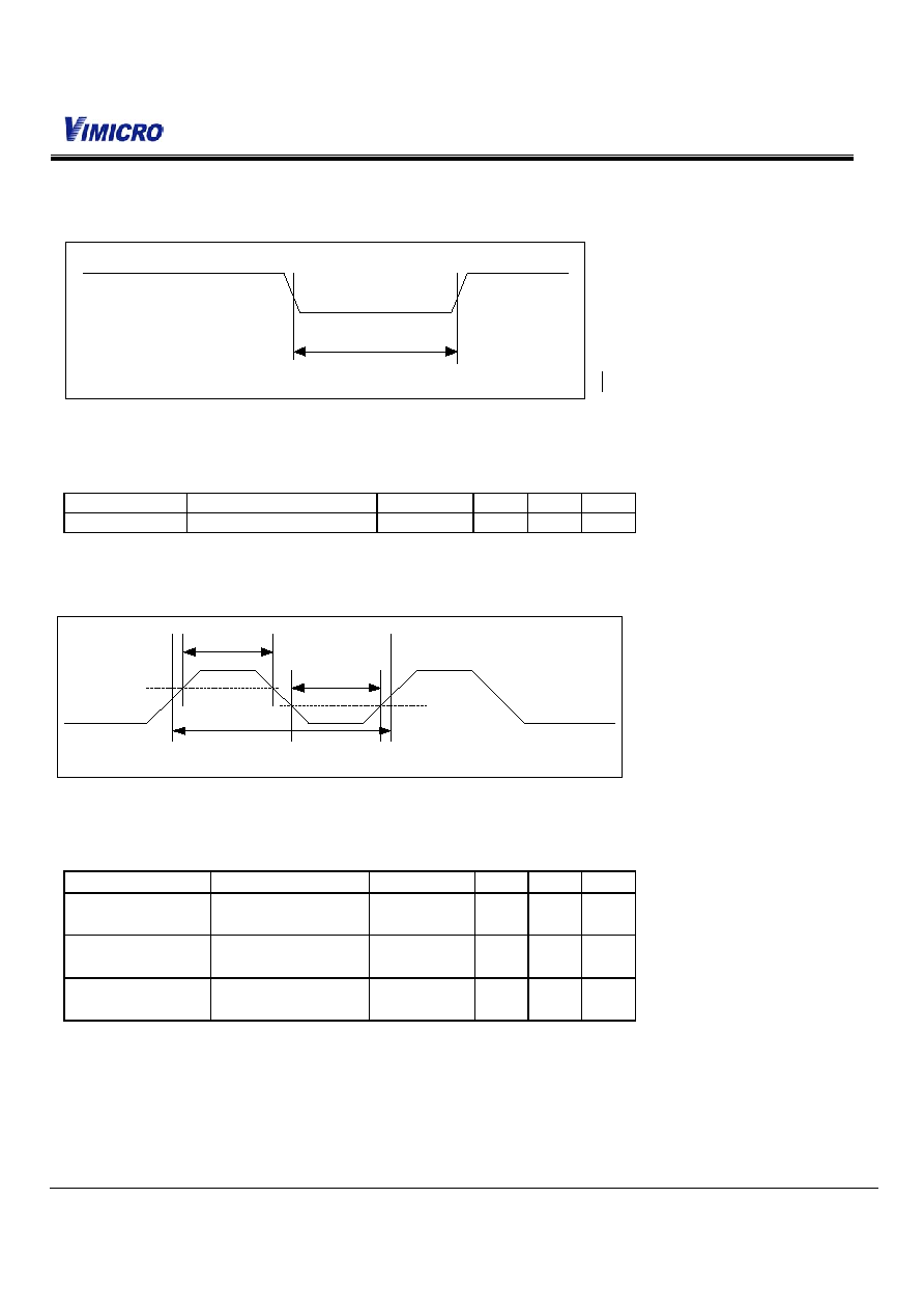
4.4. RESET Timing AC Characteristics
Reset
Trst
Figure 4 RESET Timing AC Characteristics Diagram
Table 9 Reset Signal AC Characteristics
Symbol
Parameter
Conditions Min Max Unit
Trst Reset
Pulse
Width
100
-
ms
4.5. Clock
AC
Characteristics
T
high
T
low
Tcyc
clock
Figure 5 Clock Timing AC Characteristics Diagram
Table 10 Clock Signal AC Characteristics
Symbol Parameter Conditions
Min
Max
Unit
1/Tcyc Oscillator
Frequency
48@10PPM - - Mhz
T
high
Oscillator
Clock
High Time
8.3
-
Ns
T
low
Oscillator
Clock
Low Time
8.3
-
Ns

Mar. 2002
11
ZC0301
VGA & CIF USB PC Camera Controller
4.6. Input Signal AC Characteristics
valid data
T
su
T
h
clock
data input
Figure 6 Input Signal Timing AC Characteristics Diagrams
Table 11 Input Signal AC Characteristics
Symbol Parameter
Conditions
Min Max Unit
T
su
Input setup time
18
-
ns
T
h
Input hold time
0
-
ns
5. Register Table (Vendor Commands)
Table 12 System Control Register
Address Symbol
Register
Name
Default
Access
0180H SysCon
System
control
register
00H R/W
0181H
SysOp
System enable register
00H
R/W
0183H
ImWidthH
Image width high byte
02H
R/W
0184H
ImWidthL
Image width low byte
80H
R/W
0185H
ImHeightH
Image height high byte
01H
R/W
0186H
ImHeightL
Image height low byte
E0H
R/W
0187H TbrcReg
JPEG
BRC
register
00H R/W
0188H QuanReg
JPEG
Quantization
register
00H R/W
0189H
LEVEL1_ADDR
Target image size for state 1
40H
R/W
018AH
LEVEL2_ADDR
Target image size for state 2
60H
R/W
018BH
LEVEL3_ADDR
Target image size for state 3
80H
R/W
018DH CustomID
Custom
ID
RO
018EH FrameConEn
Frame
Control
Enable
01H
R/W
018FH
Frame State
Frame Control State
RO
0190H
LEVEL1Data_add
Hblank value for state 1
0AH
R/W
0191H
LEVEL2Data_add
Hblank value for state 2
1BH
R/W
0192H
LEVEL3Data_add
Hblank value for state 3
3CH
R/W

Mar. 2002
12
ZC0301
VGA & CIF USB PC Camera Controller
6. Mechanical Information
Figure 7 28-Pin PLCC Package Diagram
Table 13 ZC
0301
Package Dimension
Lead Count
28
D1 453
Body Size
E1 453
Stand-Off A1
20
Body Thickness
A2
150
Lead Width
b
17
Lead Thickness
c
10
Lead Pitch
e
50
Unit: mil (1mil = 1/1000 inch)

Mar. 2002
13
ZC0301
VGA & CIF USB PC Camera Controller
Appendix I Sensor Interface Description
ZC0301 supports Hyundai VGA format sensors (HV7131B).
1.
INPUT / OUTPUT AC CHARACTERISTICS
All output timing delays are measured with output load 60pF
Output delay includes the internal clock path delay [6ns] and output driving delay that changes in respect to
the output load, the operating environments, and a board design.
Due to the variable valid time delay of the output, output signals may be latched in the negative edge of
MCLK for the stable data transfer between the image sensor and a host for less than 15MHz operation.
2.
MCLK TO HSYNC / VSYNC Timing
F
IGURE
8.1-1 M
CLK TO
H
SYNC
/V
SYNC
T
IMING
D
IAGRAM
T1: MCLK RISING TO HSYNC/VSYNC valid maximum Time: 18ns [output load: 60pF]
T2: HSYNC/VSYNC valid Time: minimum 1 clock (subject to T1, T2 timing rule )
3.
MCLK to DATA Timing
F
IGURE
8.1-2 M
CLK TO
D
ATA
T
IMING
D
IAGRAM
T3: MCLK rising to DATA Valid maximum Time: 18ns [output load:60pF]
Note: HSYNC signal is high when valid data is on the DATA bus.
4. ENB
Timing
F
IGURE
8.1-3 E
NB
T
IMING
D
IAGRAM

Mar. 2002
14
ZC0301
VGA & CIF USB PC Camera Controller
T4: ENB Setup Time: 5[ns]
T5: ENB Hold Time: 5[ns]
T6: ENB Valid Time: minimum 2 Clock
5. RESET
Timing
Must in Valid (active low) state at least 8 MCLK periods
6. I
2
C Bus (Programming Serial Bus) Timing
F
IGURE
8.1-4 I
2
C B
US
T
IMING
D
IAGRAM
7. I
2
C Bus Interface Timing
Parameter Symbol
Min
Max.
Unit
SCK clock frequency
f
sck
0
400
KHz
Time that I
2
C bus must be free before a
new transmission can start
t
buf
1.2
-
Us
Hold time for a START
t
hd
;S
ta
1.0 - Us
LOW period of SCK
t
low
1.2
- Us
HIGH period of SCK
t
high
1.0
- Us
Setup time for START
t
su
;S
ta
1.2
- Us
Data hold time
t
hd
;d
at
1.3 - Us

Mar. 2002
15
ZC0301
VGA & CIF USB PC Camera Controller
Data setup time
t
su
;d
at
250
- Ns
Rise time of both SDA and SCK
t
r
-
250
Ns
Fall time of both SDA and SCK
t
f
-
300
Ns
Setup time for STOP
t
su
;S
tp
1.2 - Us
Capacitive load of each bus lines (SDA,
SCK)
C
b
-
-
Pf
Table 8.1 I
2
C Bus Interface Timing
8.
Connection for HV7131B
MCLK
CS_CLK
VSYNC
VSYNC
HSYNC
HSYNC
DATA[7:0]
CS_D[7:0]
SCK
SDA
SCK
SDA
3.3V
4.7K
HV7131B
ZC0301
F
IGURE
8.1-5 P
ERIPHERAL
C
ONNECTION
D
IAGRAM
Note:
1. For Hyundai sensor, RESETB is active LOW.