 | –≠–ª–µ–∫—Ç—Ä–æ–Ω–Ω—ã–π –∫–æ–º–ø–æ–Ω–µ–Ω—Ç: ZH431N802 | –°–∫–∞—á–∞—Ç—å:  PDF PDF  ZIP ZIP |
ADJUSTABLE PRECISION
ZENER SHUNT REGULATOR
Issue 2 - February 1998
ZH431
DEVICE DESCRIPTION
The ZH431 is a three terminal adjustable
s h u n t r e g u l a t o r o f f e r i n g e x c e l l e n t
temperature stability and output current
handling capability up to 30mA. The output
voltage may be set to any chosen voltage
between 2.5 and 36 volts by selection of two
external divider resistors.
The devices can be used as a replacement
for zener diodes in many applications
r e q u i r i n g a n i m p r o v e me n t i n z e n e r
performance.They are also ideal for use in
the feedback circuits of off line SMPUs as
well as many general purpose regulator and
reference applications where initial accuracy
and low temperature coefficient are key
requirements.
Note:
ZH431 is not recommended for new designs.
Refer to ZR431
FEATURES
∑
Surface mount SO8, SOT223,SOT23
and SOT89 packages
∑
TO92 package
∑
2% and 1% tolerance
∑
Maximum temperature coefficient 55
ppm/∞C
∑
Temperature compensated for
operation over the full temperature
range
∑
Programmable output voltage
∑
50
µ
A to 30mA current sink capability
∑
Low output noise
APPLICATIONS
∑
Shunt regulator
∑
Series regulator
∑
Voltage monitor
∑
Over voltage/ under voltage protection
∑
Switch mode power supplies
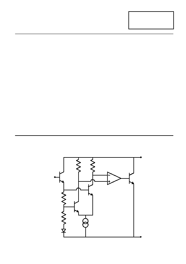
V
Z
G
nd
V
ref
SCHEMATIC DIAGRAM
4-15
ZH431
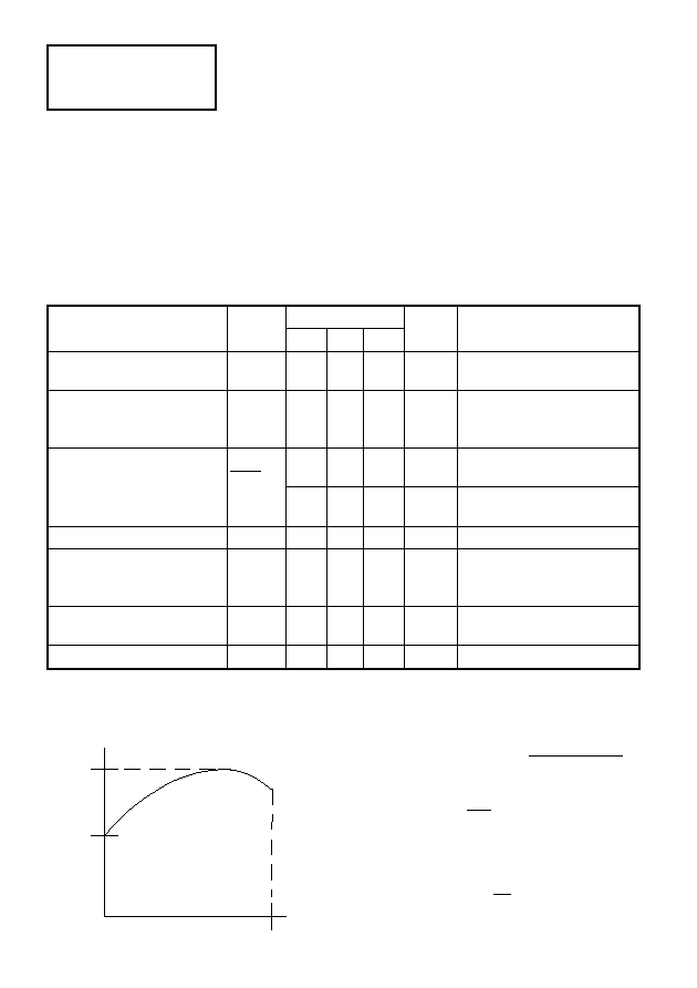
ABSOLUTE MAXIMUM RATING
Cathode Voltage (V
Z
)
40V
Cathode Current
50mA
Operating Temperature
-40 to 85∞C
Storage Temperature
-55 to 125∞C
Recommended Operating Conditions
Min
Max
Cathode Voltage
Vref
36V
Cathode Current
50
µ
A
30mA
Power Dissipation (T
amb
=25∞C, T
jmax
=150∞C)
SOT23
330mW
TO92
780mW
SOT223
2W
SO8
780mW
SOT89
1.5W
ELECTRICAL CHARACTERISTICS TEST CONDITIONS (Unless otherwise
stated):T
amb
=25∞C
PARAMETER
SYMBOL
VALUE
UNITS CONDITIONS
MIN
TYP MAX
Reference Voltage 2%
1%
V
ref
2.45
2.475
2.50
2.50
2.55
2.525
V
I
L
=10mA (Fig1), V
Z
=V
ref
Deviation of Reference
Input Voltage over
Temperature
V
dev
8.0
17
mV
I
L
=10mA, V
Z
=V
ref
T
a
=full range (Fig1)
Ratio of the change in
Reference Voltage to the
Change in Cathode
Voltage
V
ref
V
Z
-0.7
-2.7
mV/V
V
Z
from V
ref
to 10V
I
Z
=10mA (Fig2)
-0.6
-2.0
mV/V
V
Z
from 10V to 36V
I
Z
=10mA (Fig2)
Reference Input Current
I
ref
0.15 1.0
µ
A
R1=10k, R2=O/C, l
L
=10mA (Fig2)
Deviation of Reference
Input Current over
Temperature
I
ref
0.06 0.2
µ
A
R1=10k, R2=O/C, I
L
=10mA
T
a
=full range (Fig2)
Minimum Cathode
Current for Regulation
I
Zmin
21
50
µ
A
V
Z
=V
ref
(Fig1)
Dynamic Output Impedance R
Z
0.75
V
Z
=V
ref
(Fig1), f=0Hz
Deviation of reference input voltage, V
dev,
is defined as the maximum variation of the reference
input voltage over the full temperature range.
The average temperature coefficient of the reference input voltage, V
ref
is defined as:
V
ref
(
ppm
/
∞
C
)=
V
dev
x 1000000
V
ref
(
T1
-
T2
)
The dynamic output impedance, Rz, is defined as:
R
Z
=
V
Z
I
Z
When the device is programmed with two external
resistors, R1 and R2, (fig 2) , the dynamic output
impedance of the overall circuit, R', is defined as:
R
'
=
R
z
(
1
+
R1
R2
)
Vmax
Vmin
T1
T2
Vdev = Vmax - Vmin
Temperature
4-16
ZH431
Dynamic Impedance v Frequency
Frequency (Hz)
10k
100k
1M
0.01
Dyna
mic I
m
p
e
d
a
n
c
e
(
Ohms
)
0.1
100
10
1
100
1k
Power Dissipation Derating
Ambient Temperature (∞C)
100
Po
we
r
D
i
s
s
i
pation
(W)
1.0
0
25
75
2.0
50
SOT223
S08/T092
SOT23
Cathode Current v Temperature
Temperature (∞C)
0
20
60
40
12
M
i
nimum Cathod
e Curre
n
t
(uA)
14
22
20
18
16
-40
-20
80
24
26
Vref= Vz
Reference Current v Temperature
Temperature (∞C)
0
20
60
40
100
Refe
rence Cu
rr
ent
(
n
A
)
120
200
180
160
140
-40
-20
80
Change in Vref v Cathode Voltage
Cathode Voltage (V)
10
15
25
20
-25
C
h
a
n
g
e
i
n
Refe
rence V
o
l
tage
(
m
V
)
-20
0
-5
-10
-15
0
5
30
35
5
40
Vref= Vz
Iz= 10mA
1mA
10mA
Vref=Vz
TYPICAL CHARACTERISTICS
SOT89
Reference Voltage v Temperature
Temperature (∞C)
0
20
60
40
2.47
R
e
f
e
ren
ce V
o
l
tag
e (V
)
2.48
2.52
2.51
2.50
2.49
-40
-20
80
Iz= 10mA
4-17
ZH431
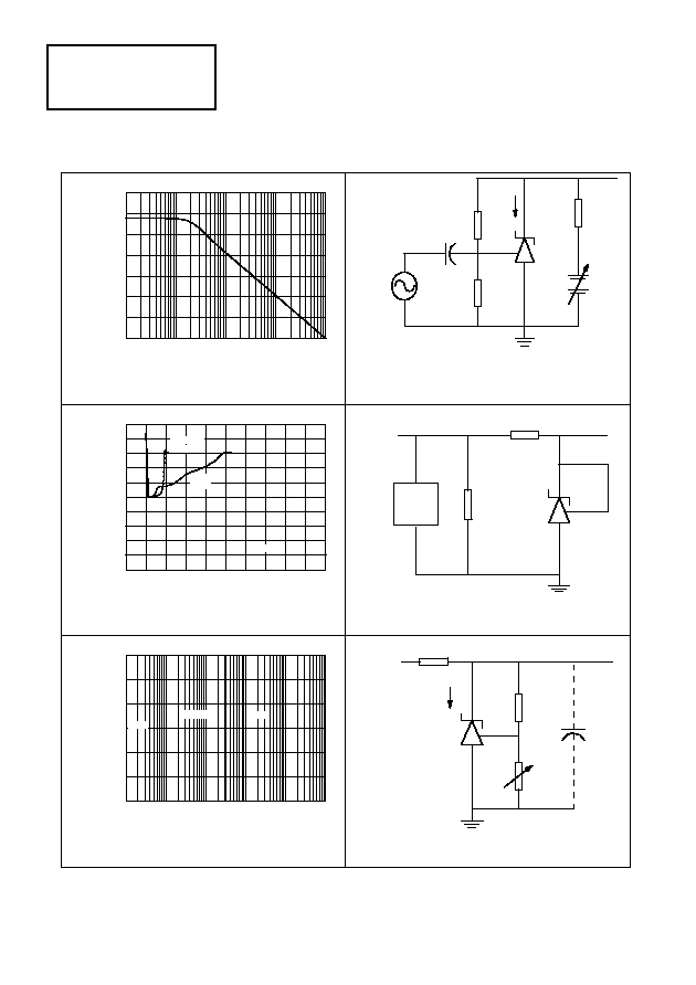
Gain v Frequency
Frequency (Hz)
100
10k
O
p
e
n
Loop
G
ain (d
B
)
0
50
100k
1M
1k
40
30
20
10
70
60
Pulse Response
Time (µs)
0.1
0.15
0.25
0.2
0
V
olta
g
e
S
wing
(V
)
5
3.0
2.0
1.0
0
0
0.05
INPUT
REPETITIVE
PULSE
SINGLE
PULSE
Stability Boundary Conditions
Load Capacitance (F)
1000p
0.01µ
0.1µ
0
C
athode C
u
r
r
ent (mA
)
5
20
15
10
10p
100p
1µ
Unstable
Stable
25
30
TYPICAL CHARACTERISTICS
Stable
I
Z
15k
V
Z
Test Circuit for Open Loop Voltage Gain
8k25
9
µ
F
230
+
-
I
Z
= 10mA,
T
A
= 25∞C
Test Circuit for Pulse Response
Input Monitor
V
Z
220
50
Pulse
Generator
T
A
= 25∞C
Test Circuit for Stability Boundary Conditions
Input
150
10k
V
ref
< V
Z
< 40, I
Z
= 10mA, T
A
= 25∞C
V
Z
I
Z
4-18
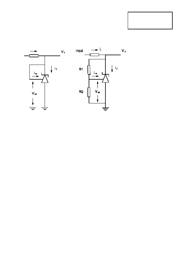
I
L
Input
Fig 1 ≠ Test Circuit for V
z
=V
ref
DC TEST CIRCUITS
Fig 2 ≠ Test Circuit for V
z
>V
ref
ZH431
4-19

APPLICATION CIRCUITS
R2
Vout = 1 +
R1
R2
Vref
SERIES REGULATOR
V+
Vout
R1
30
0.01µF
Vref
Vout = 1 +
R1
R2
Vref
Vout = Vref + Vreg
MIN
OUTPUT CONTROL OF A
THREE TERMINAL FIXED REGULATOR
R2
R1
V+
Vout
Vref
ZSR***
In
Out
Common
R2
R1
V+
Vout
Vout =
Vref
1 +
R1
R2
Vref
HIGHER CURRENT SHUNT REGULATOR
V+
OUTPUT
INPUT
V
= 2.5V
TH
V
2V
on
V
= V+
off
SINGLE SUPPLY COMPARATOR
WITH TEMPERATURE
COMPENSATED THRESHOLD
R2A
R1A
V+
Vref
R2B
R1B
Vref
1 +
R1B
R2B
Vref
OVER VOLTAGE / UNDER VOLTAGE
PROTECTION CIRCUIT
Low limit =
High limit =
1 +
R1A
R2A
Vref
R2
R1
Vout =
Vref
1 +
R1
R2
Vref
SHUNT REGULATOR
V+
Vout
OUTPUT
ZH431
4-20

ZH431
TO92 Package
Suffix ≠ C
Bottom
View
CONNECTION DIAGRAMS
SO8 Package
Suffix ≠ N8
Top
View
SOT223 Package Suffix ≠ G
Top View ≠
Pin 4 floating or connected to pin 2
SOT23 Package
Suffix ≠ F
Top
View
SOT89 Package Suffix ≠ Z
Top
View ≠
Pin 4 floating or connected to pin 2
Part Number
Package
Tol.
%
Part Mark
ZH431C01
TO92
1.0
ZH43101
ZH431C02
TO92
2.0
ZH43102
ZH431G01
SOT223
1.0
ZH43101
ZH431G02
SOT223
2.0
ZH43102
ZH431F01
SOT23
1.0
43H
ZH431F02
SOT23
2.0
43G
ZH431Z01
SOT89
1.0
43H
ZH431Z02
SOT89
2.0
43G
ZH431N801
SO8
1.0
ZH43101
ZH431N802
SO8
2.0
ZH43102
ORDERING INFORMATION
4-21