 | –≠–ª–µ–∫—Ç—Ä–æ–Ω–Ω—ã–π –∫–æ–º–ø–æ–Ω–µ–Ω—Ç: ZN428D | –°–∫–∞—á–∞—Ç—å:  PDF PDF  ZIP ZIP |

THIS DOCUMENT IS FOR MAINTENANCE
PURPOSES ONLY AND IS NOT
RECOMMENDED FOR NEW DESIGNS

AUGUST 1994
DS3007-2.1
ZN428E8/ZN428J8/ZN428D
8-BIT LATCHED INPUT D-A CONVERTER
DC16
1
2
3
4
5
6
7
BIT 3
BIT 1 (MSB)
9
10
BIT 8
NC
ANALOG OUTPUT
V
REF
IN
BIT 2
V
REF
OUT
ANALOG GROUND
11
12
13
14
BIT 7
BIT 5
BIT 4
BIT 6
+V
CC
(+5V)
1
2
3
4
5
6
7
8
9
10
11
12
13
14
15
16
ZN428J8
ZN428D
MP16 WIDE BODY
8
15
16
ENABLE
DIGITAL GROUND
ZN428E8
DP16
BIT 8
NC
ANALOG OUTPUT
V
REF
IN
V
REF
OUT
ANALOG GROUND
BIT 7
ENABLE
BIT 3
BIT 1 (MSB)
BIT 2
BIT 5
BIT 4
BIT 6
+V
CC
(+5V)
DIGITAL GROUND
Fig.1 Pin connections (not to scale) - top view
The ZN428 is a monolithic 8-bit D-A converter with input
latches to facilitate updating from a data bus. The latch is
transparent when enable is LOW and the data is held when
enable is taken HIGH. The ZN428 also contains a 2.5V
reference the use of which is pin optional to retain flexibility.
An external fixed or varying reference may therefore be
substituted.
FEATURES
s
Contains DAC with Data Latch and On-Chip
Reference
s
Guaranteed Monotonic over the Full Operating
Temperature Range
s
Single +5V Supply
s
Microprocessor Compatible
s
TTL and 5V CMOS Compatible
s
800ns Settling Time
s
Complementary to ZN427 A to D Series
s
Commercial or Military Temperature Range
ORDERING INFORMATION
Device Type
Operating temperature
Package
ZN428D
0
∞
C to +70
∞
C
MP16W
ZN428E8
0
∞
C to +70
∞
C
DP16
ZN428J8
-55
∞
C to +125
∞
C
DC16

ZN428
ABSOLUTE MAXIMUM RATINGS
Supply voltage V
CC
+7.0V
Max.voltage, logic and V
REF
inputs
+V
CC
Operating temperature range
0
∞
C to +70
∞
C (ZN428E8, ZN428D)
-55
∞
C to +125
∞
C (ZN428J8)
Storage temperature range
-55
∞
C to +125
∞
C
Analog ground to digital ground
±
200mV
Parameter
Min.
Typ.
Max.
Units
Conditions
Internal Voltage Reference
Output voltage
2.475
2.550
2.625
V
Slope resistance
-
0.5
2
V
REF OUT
T.C.
-
50
-
ppm/
∞
C
Reference current
4
-
15
mA
Note 1
D-A Converter
Linearity error
-
-
±
0.5
LSB
2.0V
V
REF IN
3.0V
Differential non-linearity
-
±
0.5
-
LSB
Linearity error T.C.
-
±
3
-
ppm/
∞
C
Differential non-linearity T.C.
-
±
6
-
ppm/
∞
C
Offset voltage
-
2
5
mV
All bits off
Offset voltage T.C.
-
±
6
-
µ
V/
∞
C
Full-scale output
2.545
2.550
2.555
Full-scale output T.C.
-
2
-
ppm/
∞
C
Analog output resistance
-
4
-
k
External reference voltage
0
-
3.0
V
Settling time to 0.5 LSB
-
-
800
1.25
-
-
ns
µ
s
1 LSB major transition
(Note 2)
All bits ON to OFF or
OFF to ON (Note 2)
Operating temperature range:
ZN428D and ZN428 E8
ZN428J8
0
-55
-
-
70
125
∞
C
∞
C
Supply voltage (V
CC
)
4.5
5.0
5.5
V
Supply current
-
20
30
mA
Note 3
Power consumption
-
100
-
mW
Note 1: See REFERENCE
Note 2: R
L
= 10M
, C
L
= 10pF
Note 3: All inputs HIGH (V
IH
= 3.5V)
ELECTRICAL CHARACTERISTICS
(V
CC
= +5V, T
amb
= 25
∞
C unless otherwise specified)
123
R
REF
= 390
C
REF
= 1
µ
F
123
External reference
V
REF
IN
= 2.560V,
all bits ON

ZN428
Parameter
Min.
Typ.
Max.
Units
Conditions
Logic
(over specified operating
temperature range)
High level input voltage
2.0
-
-
V
Low level input voltage
-
-
0.8
V
High level input current
-
-
-
-
60
20
µ
A
µ
A
V
IN
= 5.5V, V
CC
= Max.
V
IN
= 2.4V, V
CC
= Max.
Low level input current
-
-
-5
µ
A
V
IN
= 0.4V, V
CC
= Max.
Input clamp diode voltage
-
-1.5
-
V
I
IN
= -8mA
Enable pulse width
100
-
-
ns
Data set-up time
150
-
-
ns
Note 4
Data hold time
10
-
-
ns
Note 5
ELECTRICAL CHARACTERISTICS
(cont.)
Note 4: Set up time before ENABLE goes high
Note 5: Hold time after ENABLE goes high
D-A CONVERTER
The converter is of the voltage switching type and uses
an R-2R ladder network as shown in Fig.3. Each 2R element
is connected to 0V or V
REF IN
by transistor voltage switches
specially designed for low offset voltage (<1mV). A binary
weighted voltage is produced at the output of the R-2R
ladder.
Fig.3 The R-2R ladder network
Analog output =
n
(V
REF IN
- V
OS
) + V
OS
256
where n is the digital input to the D-A from the data latch.
V
OS
is a small offset voltage produced by the D-A switch
currents flowing through the package lead resistance. The
value of V
OS
is typically 1mV. This offset will normally be
removed by the setting up procedure (see Operating Notes)
and because the offset temperature coefficient is low
(
±
6
µ
V/
∞
C)the effect on accuracy is negligible.

ZN428
Fig.4 shows equivalent circuit of the output (ignoring
V
OS
). The output resistance R has a temperature coefficient
of +0.2% per
∞
C.
The gain drift due to this is
0.2R
% per
∞
C.
R+R
L
R
L
should be chosen as large as possible to make the
gain drift small. As an example if R
L
= 400k
then the gain
drift due to the T.C. of R for a 100
∞
C change in ambient
temperature will be less than 0.2%. Alternatively the ZN428
can be buffered by an amplifier (see Operating Notes).
REFERENCE
(a) Internal Reference
The internal reference is an active bandgap circuit which
is equivalent to a 2.5V Zener diode with very low slope
impedance (Fig.5). A resistor (R
REF
), should be connected
between +V
CC
(pin 10) and pin 7. The recommended value
of 390
will supply a nominal reference current of (5.0-
2.5)/0.39 = 6.4mA. A stabilising/decoupling capacitor C
REF
=
1
µ
F is required between pins 7 and 8 for internal reference
option, V
REF OUT
(pin 7) being connected to V
REF IN
(pin 6).
Fig.4 Analog output equivalent circuit
Fig.5 Internal voltage reference

ZN428
Up to five ZN428s may be driven from one internal
reference (there is no need to reduce R
REF
). This useful
feature saves power and gives excellent gain tracking
between the converters.
(b) External Reference
If required an external reference voltage may be connected
to V
REF IN
. The slope resistance of such a reference should be
less than
2.5
, where n is the number of
converters supplied.
n
V
REF IN
can be varied from 0 to +3V for ratiometric
operation. The ZN428 is guaranteed monotonic for V
REF IN
above 2V.
LOGIC
Input coding is binary for unipolar operation and offset
binary for bipolar operation. When the ENABLE input is low
the data inputs drive the D to A directly. When ENABLE goes
high the input data word is held in the data latch.
The equivalent circuit for the data and clock inputs is
shown in Fig.6.
The ZN428 is provided with separate analog and digital
ground connections. The circuit will operate correctly with as
much as
±
200mV between the two grounds.
Fig.6 Equivalent circuit of all inputs
OPERATING NOTES
(1) Unipolar D-A Converter
The nominal output range of the ZN428 is 0 to V
REF IN
through a 4
resistance. Other output ranges can readily be
obtained by using an external amplifier.
The general scheme (Fig.7) is suitable for amplifiers
with input bias currents less than 1.5
µ
A.
The resulting full-scale range is given by:
V
OUT
FS =
(
1 + R1
)
V
REF IN
= G.V
REF IN
R2
The impedance at the inverting input is R1//R2 and for
low drift with temperature this parallel combination should be
equal to the ladder resistance (4k
). The required nominal
values of R1 and R2 are given by R1 = 4Gk
and R
2
=
4G/(G-1)k
.
Using these relationships a table of nominal resistance
values for R
1
and R
2
can be constructed for V
REF IN
= 2.5V.
For gain setting R
1
is adjusted about its nominal value.
Practical circuit realisations (including amplifier stabilising
components) for +5 and +10V output ranges are given in
Fig.8. Settling time for a major transition is 1.5
µ
s typical.
Output Range
G
R
1
R
2
+5V
2
8k
8k
+10V
4
16k
5.33k

ZN428
Fig.7 Unipolar operation - basic circuit
Fig.8 Unipolar operation - component values

ZN428
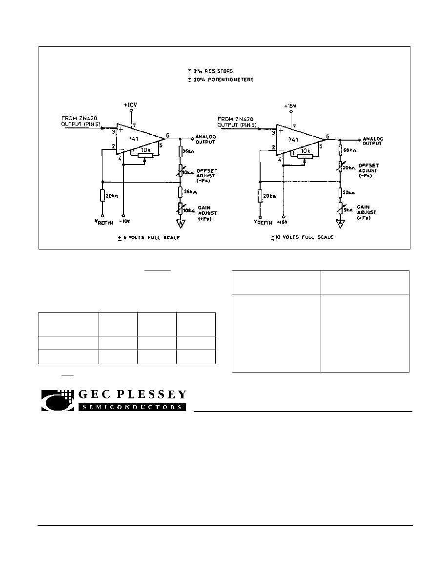
(2) Bipolar D-A Converter
For bipolar operation the output from the ZN428 is offset
by half full-scale by connecting a resistor R3 between V
REF
IN
and the inverting input of the buffer amplifier (Fig.9).
When the digital input to the ZN428 is zero the analog
output is zero and the amplifier output should be -Full-scale.
An input of all ones to the D-A will give a ZN428 output of
V
REF IN
and the amplifier output required is +Full-scale. Also,
to match the ladder resistance the parallel combination of
R
1
, R
2
and R
3
should be 4k
.
The nominal values of R
1
, R
2
and R
3
which meet these
conditions are given by
R
1
= 8Gk
, R
2
= 8G/(G-1)k
and R
3
= 8k
.
where the resultant output range is
±
G V
REF IN
. A bipolar
output range of
±
V
REF IN
(which corresponds to the basic
unipolar range 0 to V
REF IN
) is obtained if R
1
= R
3
= 8k
and
R
2
=
.
Assuming that V
REF IN
= 2.5V the nominal values of
resistors for
±
5 and
±
10V output ranges are given in the
following table:
Minus full scale (0ffset) is set by adjusting R
1
about its
nominal value relative to R
3
. Plus full-scale (gain) is set by
adjusting R
2
relative to R
1
.
Practical circuit realisations are given in Fig.10.
Note that in the
±
5V case R
3
has been chosen as 7.5k
(instead of 8.2k
) to get a more symmetrical range of
adjustment using standard potentiometers. Settling time for a
major transition is 1.5
µ
s typical.
Output Range
G
R
1
R
2
R
3
+5V
2
16k
16k
8k
+10V
4
32k
10.66k
8k
UNIPOLAR ADJUSTMENT PROCEDURE
(i) Set all bits to OFF (low) with ENABLE low and adjust
zero until V
OUT
= 0.0000V.
(ii) Set all bits ON (high) and adjust gain until V
OUT
= FS
- 1LSB.
UNIPOLAR SETTING UP POINTS
1LSB = FS
256
Output Range, +FS
LSB
FS - 1LSB
+5V
19.5 mV
4.9805V
+10V
39.1mV
9.9609V
UNIPOLAR LOGIC CODING
Input Code
(Binary)
Analog Output
(Nominal Value)
11111111
11111110
11000000
10000001
10000000
01111111
01000000
00000001
00000000
FS - 1LSB
FS - 2 LSB
3
/
4
FS
1
/
2
FS + 1LSB
1
/
2
FS
1
/
2
FS - 1LSB
1
/
4
FS
1LSB
0
Fig.9 Bipolar operation - basic circuit
ZN428
BIPOLAR ADJUSTMENT PROCEDURE
(i) Set all bits to OFF (low) with ENABLE low and adjust
offset until the amplifier output reads -full-scale.
(ii) Set all bits ON (high) and adjust gain until the
amplifier output reads +(full-scale - 1LSB).
BIPOLAR SETTING UP POINTS
1LSB = 2FS
256
Input Range,
±
FS
LSB
-FS
+(FS -
1LSB)
±
5V
39.1 mV
-5.0000V
+4.9609V
±
10V
78.1mV
-10.0000V
9.9219V
Fig.10 Bipolar operation - component values
BIPOLAR LOGIC CODING
Input Code
(Offset Binary)
Analog Output
(Nominal Value)
11111111
11111110
11000000
10000001
10000000
01111111
01000000
00000001
00000000
+(FS - 1LSB)
+(FS - 2 LSB)
+
1
/
2
FS
+ 1LSB
0
-1 LSB
-
1
/
2
FS
-(FS - 1LSB)
-FS
HEADQUARTERS OPERATIONS
GEC PLESSEY SEMICONDUCTORS
Cheney Manor, Swindon,
Wiltshire, United Kingdom. SN2 2QW
Tel: (0793) 518000
Fax: (0793) 518411
GEC PLESSEY SEMICONDUCTORS
P.O. Box 660017,
1500 Green Hills Road,
Scotts Valley, California 95067-0017,
United States of America.
Tel (408) 438 2900
Fax: (408) 438 5576
CUSTOMER SERVICE CENTRES
∑ FRANCE & BENELUX Les Ulis Cedex Tel: (1) 64 46 23 45 Fax: (1) 64 46 06 07
∑ GERMANY Munich Tel: (089) 3609 06-0 Fax: (089) 3609 06-55
∑ ITALY Milan Tel: (02) 66040867 Fax: (02)66040993
∑ JAPAN Tokyo Tel: (03) 5276-5501 Fax: (03) 5276-5510
∑ NORTH AMERICA Scotts Valley, USA Tel: (408) 438 2900 Fax: (408) 438 7023
∑ SOUTH EAST ASIA Singapore Tel: (65) 3827708 Fax: (65) 3828872
∑ SWEDEN Stockholm Tel: 46 8 702 97 70 Fax: 46 8 640 47 36
∑ TAIWAN, ROC Taipei Tel: 886 2 5461260 Fax: 886 2 7190260
∑ UK, EIRE, DENMARK, FINLAND & NORWAY
Swindon Tel: (0793) 518510 Fax: (0793) 518582
These are supported by Agents and Distributors in major countries world-wide.
© GEC Plessey Semiconductors 1994 Publication No. DS3007 Issue No. 2.1 August 1994
TECHNICAL DOCUMENTATION - NOT FOR RESALE. PRINTED IN UNITED KINGDOM
This publication is issued to provide information only which (unless agreed by the Company in writing) may not be used, applied or reproduced for any purpose nor form part of any order or contract nor to be
regarded as a representation relating to the products or services concerned. No warranty or guarantee express or implied is made regarding the capability, performance or suitability of any product or service. The