 | ÐлекÑÑоннÑй компоненÑ: ZN429D | СкаÑаÑÑ:  PDF PDF  ZIP ZIP |
Äîêóìåíòàöèÿ è îïèñàíèÿ www.docs.chipfind.ru

THIS DOCUMENT IS FOR MAINTENANCE
PURPOSES ONLY AND IS NOT
RECOMMENDED FOR NEW DESIGNS
MAY 1994
DS3008-2.0
ZN429E8/ZN429D
LOW COST 8-BIT D-A CONVERTER
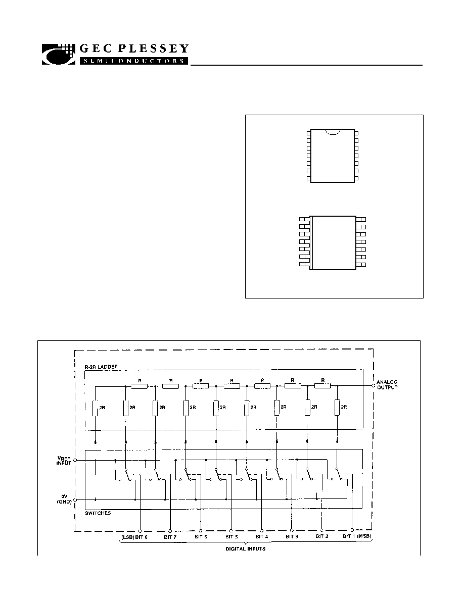
DP14
1
2
3
4
5
6
7
BIT 6
BIT 8 (LSB)
9
10
BIT 2
(MSB) BIT 1
ANALOG OUTPUT
V
REF
IN
BIT 7
NC
0V
11
12
13
14
BIT 3
BIT 4
BIT 5
+V
CC
(+5V)
NC
1
2
3
4
5
6
7
8
BIT 6
BIT 8
9
10
BIT 3
BIT 2
BIT 1
ANALOG OUTPUT
BIT 7
V
REF
IN
+V
CC
11
12
13
14
GROUND
NC
BIT 4
BIT 5
GROUND
8
ZN429E8
ZN429D
MP14
Fig.1 Pin connections (not to scale) - top view
The ZN429 is a monolithic 8-bit D-A converter
containing an R-2R ladder network of diffused resistors with
precision bipolar switches.
FEATURES
s
Linearity Error
±
1
/
2
LSB
s
Single +5V Supply
s
Low Power Consumption 25mW Typical
s
Settling Time 1 Microsecond Typical
s
TTL and 5V CMOS Compatible
s
Designed for Low Cost Applications
ABSOLUTE MAXIMUM RATINGS
ORDERING INFORMATION
Supply voltage, V
CC
+7.0V
Max. voltage, logic and V
REF
inputs
+5.5V
Storage temperature range
-55
°
C to +125
°
C
Ambient operating temperature
-40
°
C to +85
°
C
Package, ZN429D
MP14
Package, ZN429E8
DP14

ZN429
NOTE 1: Monotonic over full temperature range.
Parameter
Symbol
Min.
Typ.
Max.
Units
Conditions
Converter
Resolution
8
-
-
bits
Accuracy
8
-
-
bits
Non-linearity
-
-
±
0.5
LSB
Differential non-linearity
-
±
0.5
-
LSB
Note 1
Settling time to 0.5LSB
-
1.0
-
µ
s
1 LSB step
Settling time to 0.5LSB
-
2.0
-
µ
s
All bits ON to OFF
or OFF to ON
Offset voltage ZN429E8, ZN429D
V
OS
-
3.0
5.0
mV
All bits OFF
V
OS
temperature coefficient
-
5
-
µ
V/
°
C
Full-scale output
2.545
2.550
2.555
V
All bits ON
Ext. V
REF
= 2.56V
Full-scale temp. coefficient
-
3
-
ppm/
°
C
Ext. V
REF
= 2.560V
Non-linearity temp. coefficient
-
7.5
-
ppm/
°
C
Relative to F.S.R.
Analog output resistance
R
O
-
10
-
k
External reference voltage
0
-
3.0
V
Supply voltage
V
CC
4.5
-
5.5
V
Supply current
I
S
-
5
9
mA
High level input voltage
V
IH
2.0
-
-
V
Low level input voltage
V
IL
-
-
0.7
V
High level input current
I
IH
-
-
10
µ
A
V
CC
= max.
V
I
= 2.4V
-
-
100
µ
A
V
CC
= max.
V
I
= 5.5V
Low level input current
I
IL
-
-
-0.18
mA
V
CC
= max.
V
I
= 0.3V
ELECTRICAL CHARACTERISTICS
(at T
amb
= 25
°
C and V
CC
= +5V unless otherwise specified)
INTRODUCTION
The ZN429 is an 8-bit D-A converter. It contains an
advanced design of R-2R ladder network and an array of
precision bipolar switches on a single monolithic chip.
The special design of the ladder network results in full
8-bit accuracy using normal diffused resistors.
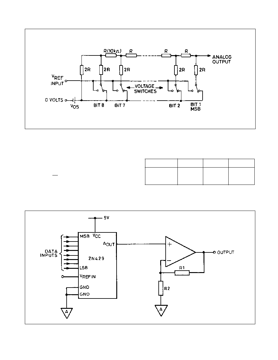
The converter is of the voltage switching type and uses
an R-2R resistor ladder network as shown in Fig.3.
Each 2R element is connected either to 0V or V
REF
by
transistor switches specially designed for low offset voltage
(typically 1mV).
Binary weighted voltages are produced at the output of
the R-2R ladder, the value depending on the digital number
applied to the bit inputs.
An external fixed or varying reference is required which
should have a slope resistance less than 2
.
Suggested external reference sources are the ZN404 or
one of the ZN458 range. Each ZN404 is capable of supplying
up to five ZN429 circuits and this is increased to ten for the
ZN458 range.
ZN429
Fig.3 The R-2R ladder network
APPLICATIONS
(1) Unipolar D-A Converter
The nominal output range of the ZN429 is 0 to V
REF IN
through a 10
resistance. Other output ranges can readily
be obtained by using an external amplifier.
The resulting full-scale range is given by
V
OUT
FS
=
(
1 + R1
)
V
REF IN
= G.V
REF IN
R2
The impedance at the inverting input is R1//R2 and for
low drift with temperature this parallel combination should be
equal to the ladder resistance (10k
). The required nominal
values of R1 and R2 are given by
R1 = 10Gk
and R
2
= 10G/(G-1)k
.
Using these relationships a table of nominal resistance
values for R
1
and R
2
can be constructed for V
REF IN
= 2.5V.
For gain setting R
1
is adjusted about its nominal value.
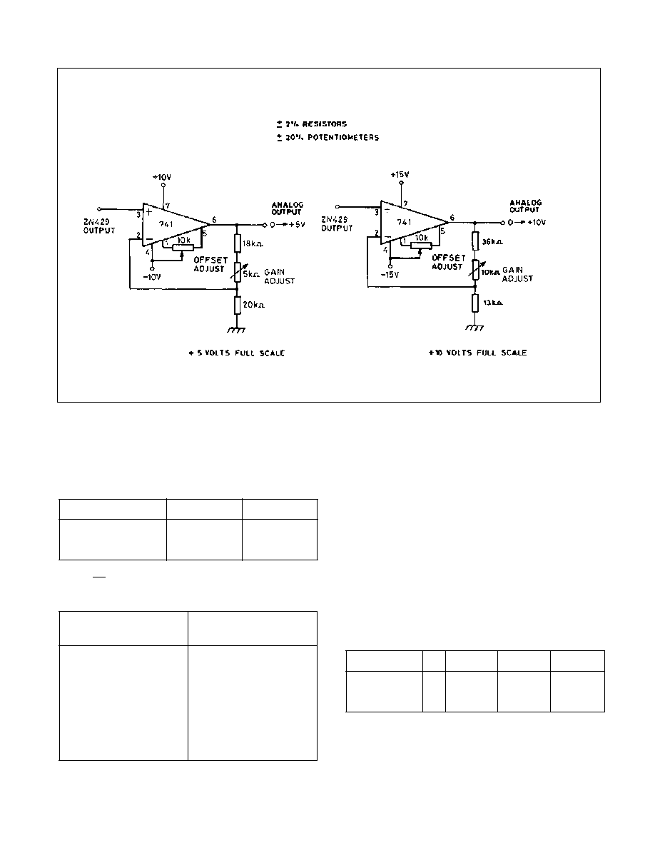
Practical circuit realisations (including amplifier stabilising
components) for +5 and +10V output ranges are given in
Fig.5. Settling time for a major transition is 2.5
µ
s typical.
Output Range
G
R
1
R
2
+5V
2
20k
20k
+10V
4
40k
13.33k
Fig.4 Unipolar operation - basic circuit
ZN429
UNIPOLAR ADJUSTMENT PROCEDURE
(i) Set all bits to OFF (LOW) and adjust zero until V
OUT
=
0.0000V.
(ii) Set all bits ON (HIGH) and adjust gain until V
OUT
=
FS - 1LSB.
UNIPOLAR SETTING UP POINTS
1LSB = FS
256
UNIPOLAR LOGIC CODING
Output Range, +FS
LSB
FS - 1LSB
+5V
19.5 mV
4.9805V
+10V
39.1mV
9.9609V
Input Code
(Binary)
Analog Output
(Nominal Value)
11111111
11111110
11000000
10000001
10000000
01111111
01000000
00000001
00000000
FS - 1LSB
FS - 2 LSB
3
/
4
FS
1
/
2
FS + 1LSB
1
/
2
FS
1
/
2
FS - 1LSB
1
/
4
FS
1LSB
0
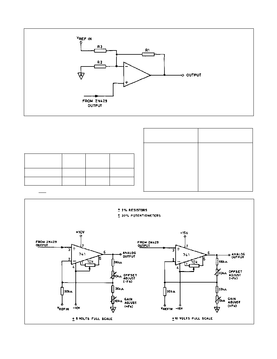
(2) Bipolar D-A Converter
For bipolar operation the output from the ZN429 is offset
by half full-scale by connecting a resistor R3 between V
REF
IN
and the inverting input of the buffer amplifier (Fig.6).
When the digital input of the ZN429 is zero the analog
output is zero and the amplifier output should be -full-scale.
An input of all ones to the D-A will give a ZN429 output of
d
V
REF IN
and the amplifier output required is +full-scale. Also,
to match the ladder resistance the parallel combination of
R
1
, R
2
and R
3
should be 10k
.
The nominal values of R
1
, R
2
and R
3
which meet these
conditions are given by
R1 = 20Gk
, R2 = 20G/(G-1)k
and R3 = 20k
.
where the resultant output range is
±
G.V
REF IN
.
Assuming that V
REF IN
= 2.5V the nominal values of
resistors for
±
5 and
±
10V output ranges are given in the
following table:
Minus full scale (0FFSET) is set by adjusting R1 about
its nominal value relative to R3. Plus full-scale (GAIN) is set
by adjusting R2 relative to R1.
Settling time for a major transistion is 2.5
µ
s typical.
Output Range
G
R
1
R
2
R
3
±
5V
2
40k
40k
20k
±
10V
4
80k
26.67k
20k
Fig.5 Unipolar operation - component values
ZN429
BIPOLAR LOGIC CODING
Input Code
(Offset Binary)
Analog Output
(Nominal Value)
11111111
11111110
11000000
10000001
10000000
01111111
01000000
00000001
00000000
+(FS - 1LSB)
+(FS - 2 LSB)
+
1
/
2
FS
+ 1LSB
0
-1 LSB
-
1
/
2
FS
-(FS - 1LSB)
-FS
Fig.6 Bipolar operation - basic circuit
BIPOLAR ADJUSTMENT PROCEDURE
(i) Set all bits to OFF (LOW) and adjust OFFSETuntil the
amplifier output reads -FULL-SCALE.
(ii) Set all bits ON (HIGH) and adjust gain until the
amplifier reads +(FULL-SCALE - 1LSB).
BIPOLAR SETTING UP POINTS
1LSB = 2FS
256
Input Range,
±
FS
LSB
-FS
+(FS -
1LSB)
±
5V
39.1 mV
-5.0000V
+4.9609V
±
10V
78.1mV
-10.0000V
9.9219V
Fig.7 Bipolar operation - component values

ZN429
HEADQUARTERS OPERATIONS
GEC PLESSEY SEMICONDUCTORS
Cheney Manor, Swindon,
Wiltshire, United Kingdom. SN2 2QW
Tel: (01793) 518000
Fax: (01793) 518411
GEC PLESSEY SEMICONDUCTORS
P.O. Box 660017,
1500 Green Hills Road,
Scotts Valley, California 95067-0017,
United States of America.
Tel (408) 438 2900
Fax: (408) 438 5576
CUSTOMER SERVICE CENTRES
· FRANCE & BENELUX Les Ulis Cedex Tel: (1) 64 46 23 45 Fax: (1) 64 46 06 07
· GERMANY Munich Tel: (089) 3609 06-0 Fax: (089) 3609 06-55
· ITALY Milan Tel: (02) 66040867 Fax: (02)66040993
· JAPAN Tokyo Tel: (03) 5276-5501 Fax: (03) 5276-5510
· NORTH AMERICA Scotts Valley, USA Tel: (408) 438 2900 Fax: (408) 438 7023
· SOUTH EAST ASIA Singapore Tel: (65) 3827708 Fax: (65) 3828872
· SWEDEN Stockholm Tel: 46 8 702 97 70 Fax: 46 8 640 47 36
· TAIWAN, ROC Taipei Tel: 886 2 5461260 Fax: 886 2 7190260
· UK, EIRE, DENMARK, FINLAND & NORWAY
Swindon Tel: (01793) 518510 Fax: (01793) 518582
These are supported by Agents and Distributors in major countries world-wide.
© GEC Plessey Semiconductors 1994 Publication No. DS3008 Issue No. 2.0 May
1994
TECHNICAL DOCUMENTATION - NOT FOR RESALE. PRINTED IN UNITED KINGDOM
This publication is issued to provide information only which (unless agreed by the Company in writing) may not be used, applied or reproduced for any purpose nor form part of any order or contract nor to be
regarded as a representation relating to the products or services concerned. No warranty or guarantee express or implied is made regarding the capability, performance or suitability of any product or service. The