WR (START CONVERSION)
BUSY (END OF CONVERSION)
DB
0
(LSB)
RD (OUTPUT ENABLE)
DB
1
CLOCK
DB
2
DB
3
R
EXT
DB
4
V
IN
DB
5
V
REF
IN
DB
6
V
REF
OUT
DB
7
(MSB)
GROUND
+V
CC
(+5V)
18
1
17
2
16
3
15
4
14
5
13
6
12
7
11
8
10
9
WR (START CONVERSION)
BUSY (END OF CONVERSION)
DB
0
(LSB)
RD (OUTPUT ENABLE)
DB
1
CLOCK
DB
2
DB
3
R
EXT
DB
4
V
IN
DB
5
V
REF
IN
DB
6
V
REF
OUT
DB
7
(MSB)
GROUND
+V
CC
(+5V)
18
1
17
2
16
3
15
4
14
5
13
6
12
7
11
8
10
9
0
�
C to +70
�
C
0
�
C to +70
�
C
0
�
C to +70
�
C
0.5
1
1
ZN448/ZN449
8-BIT MICROPROCESSOR COMPATIBLE A-D CONVERTER
DS3013 - 2.2
The ZN448 and ZN449 are 8-bit successive
approximation A-D converters designed to be easily
interfaced to microprocessors. All active circuitry is contained
on-chip including a clock generator and stable 2.5V bandgap
reference, control logic and double buffered latches with
reference.
Only a reference resistor and capacitor, clock resistor and
capacitor and input resistors are required for operation with
either unipolar or bipolar input voltage.
FEATURES
s
Easy Interfacing to Microprocessor, or operates as a
'Stand-Alone' Converter
s
Fast: 9 microseconds Conversion time Guaranteed
s
Choice of Linearity: 0.5 LSB - ZN448, 1 LSB - ZN449
s
On-Chip Clock
s
Choice of On-Chip or External Reference Voltage
s
Unipolar or Bipolar Input Ranges
s
Commercial Temperature Range
ORDERING INFORMATION
Device type
ZN448E
ZN449D
ZN449E
Package
DP18
MP18
DP18
Operating
temperature
Linearity
error (LSB)
ZN448/9E (DP18)
ZN449D (MP18)
Fig.1 Pin connection - top view
Fig.2 System diagram
SUCCESSIVE
APPROXIMATION REGISTER
3-STATE BUFFERS
8-BIT DAC
2.5V
REFERENCE
CLOCK
GENERATOR
INTERFACE
AND
CONTROL
LOGIC
+
-
CK RC OR
EXT CLOCK
3
REXT
5
WR
4
BUSY
1
RD
2
18
17
16
15
14
13
12
DB0
11
DB7
VCC (+5V)
10
GROUND
9
VREF OUT
8
VREF IN
7
ANALOGUE
INPUT
6
COMPARATOR

ZN448/9
2
DP package
V
REF
= 2.560V
MP package
DP package
V
REF
= 2.560V
V
IN
= +3V, R
EXT
= 82k
V - = -5V
R
REF
= 390
C
REF
= 4
�
7
ABSOLUTE MAXIMUM RATINGS
Supply voltage V
CC
+7
Max. voltage, logic and V
REF
input
+V
CC
Operating temperature range
0
�
C to +70
�
C (MP and DP package)
Storage temperature range
-55
�
C to +125
�
C
-
-
12
2.545
-
-
7
10
2.542
8
-
-
-
-
1
4.5
-
-
-
-
25
-3
-0.5
2.520
2.520
-
-
4
-
-
15
2.550
-
-
12
15
2.550
-
�
3
�
6
�
2.5
�
8
-
5
25
125
1
100
65
-5
-
2.550
2.550
0.5
50
-
�
0.5
�
0.75
18
2.555
�
1
�
1
17
20
2.558
-
-
-
-
-
3
5.5
40
200
-
-
150
-30
+3.5
2.580
2.600
2
-
15
Min.
Typ.
Max.
LSB
LSB
mV
V
LSB
LSB
mV
mV
V
bits
ppm/
�
C
ppm/
�
C
ppm/
�
C
�
V/
�
C
V
V
mA
mW
�
A
k
�
A
V
V
V
ppm/
�
C
mA
Parameter
Units
Conditions
ELECTRICAL CHARACTERISTICS
(at V
CC
= 5V, T
amb
= 25
�
C and f
CLK
= 1.6MHz unless otherwise specified).
ZN448
Linearity error
Differential linearity error
Zero transition
(00000000
00000001)
Full-scale
transition
(11111110 11111111)
ZN449
Linearity error
Differential linearity error
Zero transition
(00000000
00000001)
Full-scale
transition
(11111110 11111111)
All Types
Resolution
Linearity temperature coefficient
Differential linearity temperature coefficient
Full-scale temperature coefficient
Zero temperature coefficient
Reference input range
Supply voltage
Supply current
Power consumption
Comparator
Input current
Input resistance
Tail current
Negative supply
Input voltage
On-chip reference
Output voltage
ZN448
ZN449
Slope resistance
V
REF
temperature coefficient
Reference current

ZN448/9
3
ELECTRICAL CHARACTERISTICS
(Cont.)
V
IN
= +4V, V
CC
= MAX
V
IN
= +0.8V, V
CC
= MAX
V
IN
= +2.4V, V
CC
= MAX
V
IN
= +0.4V, V
CC
= MAX
V
IN
= +2.4V, V
CC
= MAX
V
IN
= +0.4V, V
CC
= MAX
I
OH
= +2.4V, V
CC
= MAX
I
OL
= +0.4V, V
CC
= MAX
V
OUT
= +2V
-
-
-
0.9
500
4
-
-
-
2
-
-
-
2
-
-
-
2.4
-
-
-
-
-
-
180
60
80
60
200
-
-
+0.5
-
-
-
-
-
-
-
-
-
300
�
10
-
-
+150
-300
-
-
-
-
-
-
180
210
80
110
80
-
-
1
-
2
1
-
-
0.8
800
-500
-
0.8
-
-
-
0.8
-
-
-
0.4
-100
1.6
2
-1.5
250
260
100
140
100
-
250
Min.
Typ.
Max.
MHz
%/
�
C
k
MHz
ns
V
V
�
A
�
A
V
V
�
A
�
A
V
V
�
A
�
A
V
V
�
A
mA
�
A
V
ns
ns
ns
ns
ns
ns
ns
Parameter
Units
Conditions
Clock
On-chip clock frequency
Clock frequency temperature coefficient
Clock resistor
Maximum external clock frequency
Clock pulse width
High level input voltage V
IH
Low level input voltage V
IL
High level input current I
IH
Low level input current I
IL
Logic (over operating temperature range)
Convert input
High level input voltage V
IH
Low level input voltage V
IL
High level input current I
IH
Low level input current I
IL
RD
input
High level input voltage V
IH
Low level input voltage V
IL
High level input current I
IH
Low level input current I
IL
High level output voltage V
OH
Low level output voltage V
OL
High level output current I
OH
Low level output current I
OL
Three-state disable output leakage
Input clamp diode voltage
RD
input to data output
Enable/disable delay times T
E1
T
E0
T
D1
T
D0
Convert pulse width t
WR
WR
input to
BUSY
output
GENERAL CIRCUIT OPERATION
The ZN448/9 utilises the successive approximation
technique. Upon receipt of a negative-going pulse at the
WR
input the
BUSY
output goes low, the MSB is set to 1 and all
other bits are set to 0, which produces an output voltage of
V
REF/2
from the DAC. This is compared to the input voltage V
IN
;
a decision is made on the next negative clock edge to reset the
MSB to 0 if < V
IN
or leave it set to 1 if < V
IN
.
Bit 2 is set to 1 on the same clock edge, producing an output
from the DAC of or + depending on the state
of the MSB. This voltage is compared to V
IN
and on the next
clock edge a decision is made regarding bit 2, whilst bit 3 is set
to 1. This procedure is repeated for all eight bits. On the eighth
negative clock edge
BUSY
goes high indicating that the
conversion is complete.
V
REF
2
V
REF
2
V
REF
4
V
REF
2
V
REF
4
During a conversion the RD input will normally be held high to
keep the three-state buffers in their high impedance state.
Data can be read out by taking
RD
low, thus enabling the
three-state output. Readout is non-destructive.
CONVERSION TIMING
The ZN448/9 will accept a low-going CONVERT pulse, which
can be completely asynchronous with respect to the clock,
and will produce valid data between 7.5 and 8.5 clock pulses
later depending on the relative timing of the clock and
CONVERT signals. Timing diagrams for the conversion are
shown in Fig.3.
The converter is cleared by a low-going CONVERT pulse,
which sets the most significant bit and results all the other bits
and the
BUSY
flag. Whilst the CONVERT input is low the MSB
output of the DAC is continuously compared with the analogue
input, but otherwise the converter is inhibited.

ZN448/9
4
After the CONVERT input goes high again the MSB decision
is made and the successive approximation routine runs to
completion.
The CONVERT pulse can be as short as 200ns; however the
MSB must be allowed to settle for at least 550ns before the
MSB decision is made. To ensure that this criterion is met
even with short CONVERT pulses the converter waits, after
the CONVERT input goes high, for a rising clock edge followed
by a falling clock edge, the MSB decision being taken on the
falling clock edge. This ensures that the MSB is allowed to
settle for at least half a clock period, or 550ns at maximum
clock frequency. The CONVERT input is not locked out during
a conversion and if it is oulsed low at any time the converter
will restart.
The
BUSY
output goes high simultaneously with the LSB
decision, at the end of a conversion indicating data valid. Note
that if the three-state data outputs are enabled during a
conversion the valid data will be available at the outputs after
the rising edge of the
BUSY
signal. If, however the outputs are
not enabled until after
BUSY
goes high then the data will be
subject to the propagation delay of the three-state buffers.
(See under DATA OUTPUTS).
Fig.3 ZN448/9 timing diagram

ZN448/9
5
If a free-running conversion is required, then the converter can
be made to cycle by inverting the
BUSY
output and feeding it
to
WR
. To ensure that the converter starts reliably after power-
up an initial start pulse is required. This can be ensured by
using a NOR gate instead of an inverter and feeding it with a
positive-going pulse which can be derived from a simple RC
network that gives a single pulse when power is applied, as
shown in Fig.4a.
The ADC will complete a conversion on every eighth clock
pulse, with the
BUSY
output going high for a period
determined by the propagation delay of the NOR gate, during
which time the data can be stored in a latch. The time available
for storing data can be increased by inserting delays into the
inverter path.
A timing diagram for the continuous conversion mode is
shown in Fig.3b.
As the
BUSY
output uses a passive pull-up the rise time of this
output depends on the RC time constant of the pull-up resistor
and load capacitance. In the continuous conversion mode the
use of a 4k7 external pull-up resistor is recommended to
reduce the risetime and ensure that a logic 1 level is reached.
Fig.4b Timing for continuous conversion
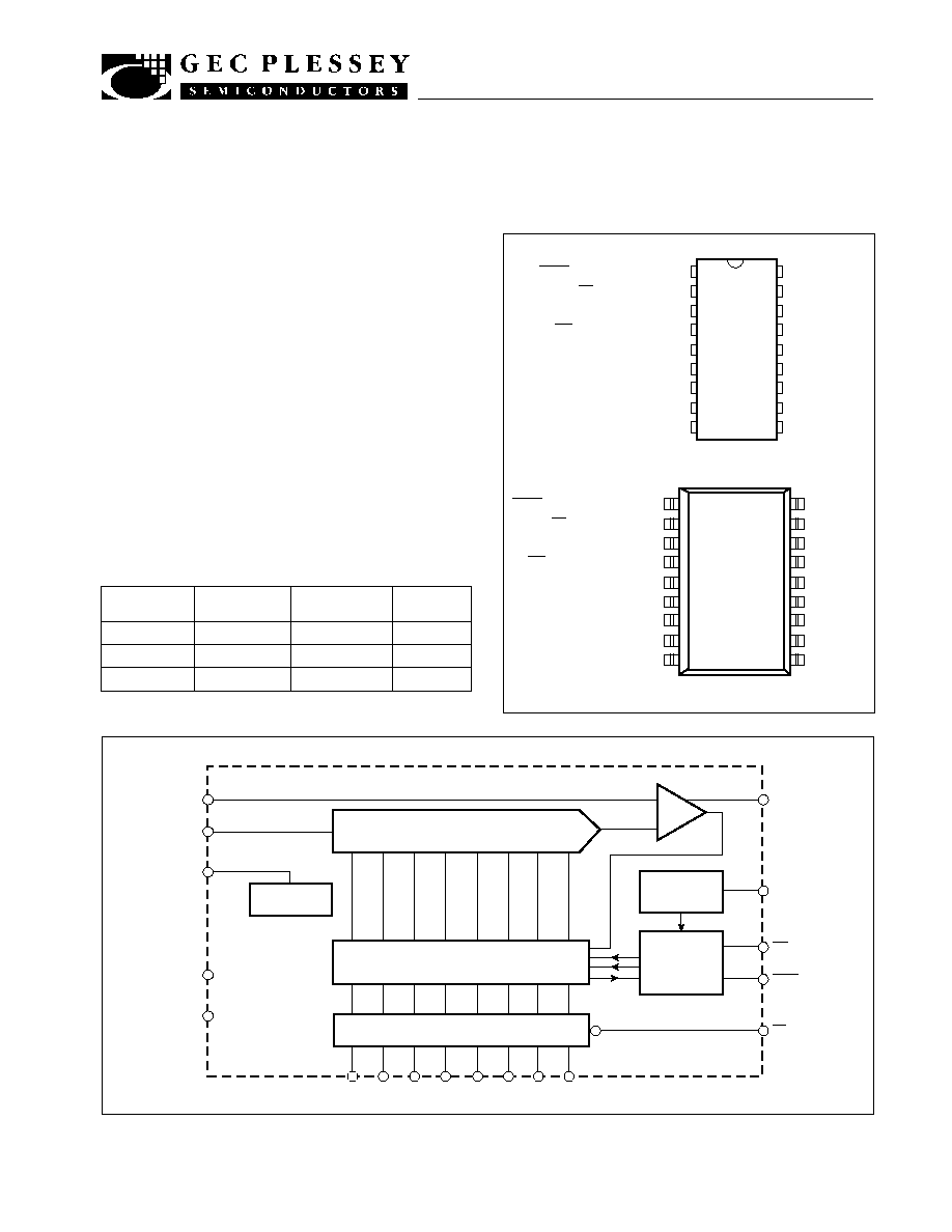
DATA OUTPUTS
The data outputs are provided with three-state buffers to allow
connection to a common data bus. An equivalent circuit is
shown in Fig.5. Whilst the
RD
input is high both output
transistors are turned off and the ZN448/9 presents only a high
impedance load to the bus.
When
RD
is low the data outputs will assume the logic states
present at the outputs of the successive register.
A test circuit and timing diagram for the output enable/disable
delays are given in Fig.6.
Fig.4a Circuit for continuous conversion
ZN448/9
6
Fig.5 Data output
20k
10k
GROUND
BITS 1-8
(PINS 11-18)
RD
(PIN 2)
VCC
500
Fig.6 Output enable/disable delays

ZN448/9
7
Fig.8 Clock circuit external components
BUSY
OUTPUT
The
BUSY
output, shown in Fig.7, utilises a passive pull-up for
CMOS/TTL compatibility. This allows up to four
BUSY
outputs
to be wire-ANDed together to form a common interrupt line.
Fig.7
BUSY
output
ON-CHIP CLOCK
The on-chip clock operates with only a single external
capacitor connected between pin 3 and ground, as shown in
Fig.8a. A graph of typical oscillator frequency versus
capacitance is given in Fig.9. The oscillator frequency may be
trimmed by means of an external resistor in series with the
capacitor, as shown in Fig.8b. However, due to processing
tolerance, the absolute clock frequency may vary
considerably between devices. For optimum accuracy and
stability of the oscillator frequency, it may be possible to use
a crystal or ceramic resonator with suitable load components,
as shown in Fig.8c. The final option is to overdrive the
oscillator input with an external clock signal from a TTL or
CMOS gate, as shown in Fig.8d.
9
3
OSC
GND
9
3
3
2k
MAX
1.2k
VCC
9
3
Xtal
1MHz
D
56pF
2200pF
D
4.7k
D
Load circuit to suit
device used
D
a) Fixed/variable capacitor
b) Fixed capacitor + variable resistor
c) Crystal or resonator
d) External TTL or CMOS drive

ZN448/9
8
Fig.10 R-2R ladder network
Fig.9 Typical clock frequency v C
CK
(R
CK
= 0)
1MHz
100kHz
10kHz
1kHz
10p
100p
1n
10n
100n
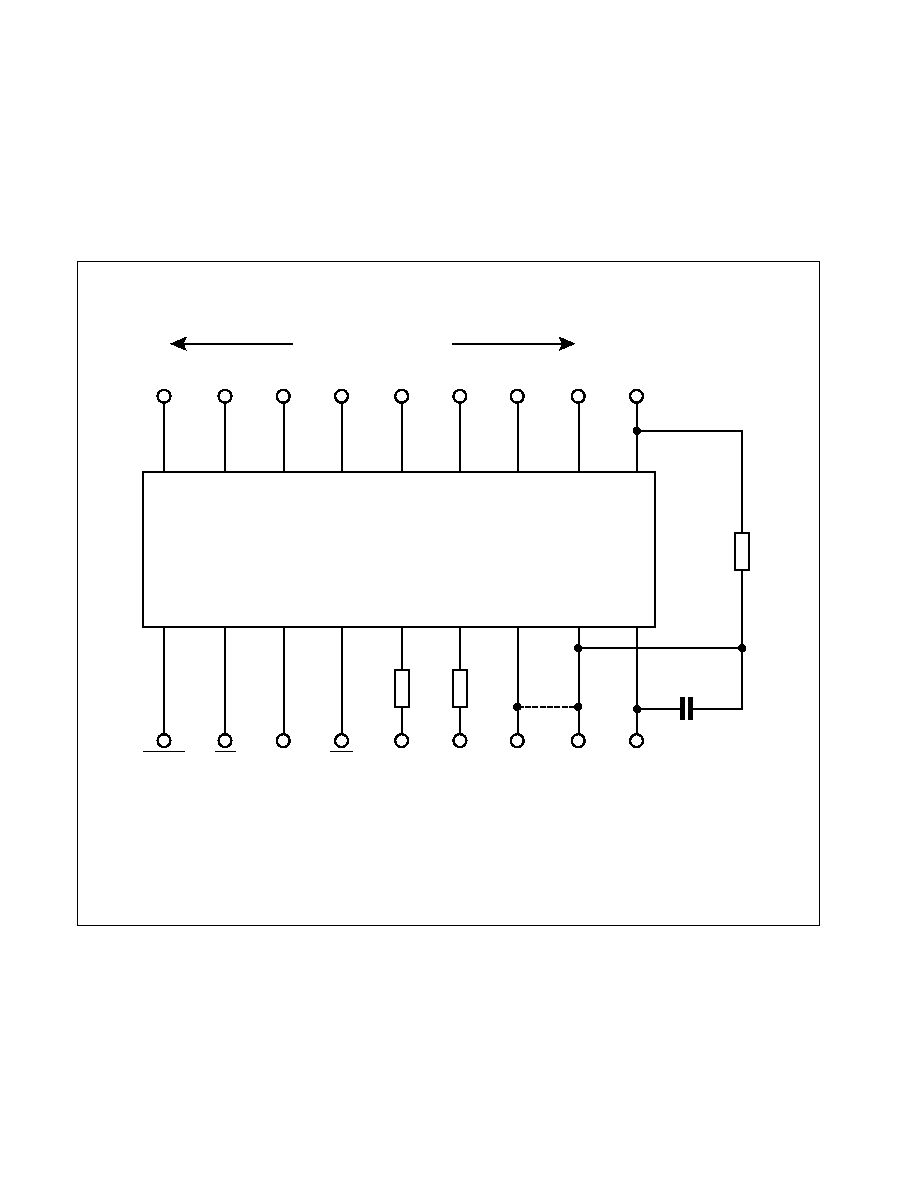
ANALOG CIRCUITS
D-A converter
The converter is of the voltage switching type and uses an R-
2R ladder network as shown in Fig.10. Each element is
connected to either 0V or V
REF IN
by transistor voltage switches
specially designed for low offset voltage (1mV).
A binary weighted voltage is produced at the output of the R-
2R ladder.
D to A output = n (V
REF IN
-V
OS
) + V
OS
256
where n is the digital input to the D-A from the successive
approximation register.
V
OS
is a small offset voltage that is produced by the device
supply current flowing in the package lead resistance. The
offset will normally be removed by the setting up procedure
and since the offset temperature coefficient is low (8
�
V/
�
C)
the effect on accuracy will be neglible.
The D-A output range can be considered to be 0 - V
REF IN
through an output resistance R (4k).
2R
2R
2R
2R
2R
R(4k)
R
R
R
D TO A OUTPUT
DB6
DB0
VOS
DB1
DB7
0 VOLTS
(PIN 9)
VREF IN
(PIN 7)
VOLTAGE
SWITCHES

ZN448/9
9
REFERENCE
(a) Internal reference
The internal reference is an active bandgap circuit which is
equivalent to a 2.5V Zener diode with a very low slope
impedance (Fig.11). A Resistor (R
REF
) should be connected
between pins 8 and 10.
The recommended value of 390
will supply a nominal
reference current of (5 - 2.5)/0.39=6.4mA. A stabilising/
decoupling capacitor, C
REF
(4
�
7), is required between pins 8
and 9. For internal reference operation V
REF OUT
(pin 8) is
connected to V
REF IN
(pin 7).
UP to five ZN448/9's may be driven from one internal
reference, there being no need to reduce R
REF
. This useful
feature saves power and gives excellent gain tracking
between the converters.
Alternatively the internal reference can be used as the
reference voltage for other external circuits and can source or
sink up to 3mA.
(b) External reference
If required an external reference in the range +1.5 to +3.0V
may be connected to V
REF IN
. The slope resistance of such a
reference source should be less than 2.5
, where n is the
n
number of converters supplied.
GROUND
(PIN 9)
CREF
(0.47�)
RREF
(390)
VREFOUT
(PIN 8)
VCC +5V
(PIN 10)
Fig.11 Internal voltage reference
RATIOMETRIC OPERATION
If the output from a transducer varies with its supply then an
external reference for the ZN4448/9 should be derived from
the same supply. The external reference can vary from +1.5
to +3.0V. The ZN448/9 will operate if V
REF IN
is less than +1.5V
but reduced overdrive to the comparator will increase its delay
and so the conversion time will need to be increased.
COMPARATOR
The ZN448/9 contains a fast comparator, the equivalent input
circuit of which is shown in Fig.12. A negative supply voltage
is required to supply the tail current of the comparator.
However as this is only 25 to 150
�
A and need not be well
stabilised it can be supplied by a simple diode pump circuit
driven from the
BUSY
output.

ZN448/9
10
Fig.12 Comparator equivalent circuit
4k
4k
PIN 5
V -
6k
6k
TO LOGIC
HIGH = 'RETAIN BIT'
D TO A OUTPUT
(O - VREFIN)
AIN
RIN
VIN
PIN 6
+5V PIN 10
REXT
IEXT
+
-
Fig.13 Diode pump circuits to supply comparator tail current

ZN448/9
11
Several suitable circuits are shown in Fig.13. The principle of
operation is the same in each case. Whilst the
BUSY
output
is high, capacitor C1 is charged to about 4-4.5V. During a
conversion the
BUSY
output goes low and the upper end of C1
is thus also pulled low. The lower end of C1 therefore applies
about -4V to R2, thus providing the tail current for the
comparator. The time constant R2. C1 is chosen according
to the clock frequency so that droop of the capacitor voltage is
not significant during a conversion.
The constraint on using this type of circuit is that C1 must be
recharged whilst the
BUSY
output is high. If the
BUSY
output
is high for greater than one converter clock period then the
circuit of Fig.13a will suffice. If this is not the case, for example,
in the continuous conversion mode, then the circuits of Figs.
13b and 13c are recommended, since these can pump more
current into the capacitor.
Where several ZN448/9's are used in a system the self-
oscillating diode pump circuit Fig.14 is recommeded.
Alternatively, if a negative supply is available in the system
then this may be utilised. A list of suitable resistor values for
different supply voltages is given in Table 1.
Fig.14 Diode pump circuit to supply comparator tail current for up to five ZN448/9's
22n
330
5V
470
100n
100n
IN914
IN914
-3.5V
V � (volts)
3
5
10
12
15
20
25
30
R
EXT
(k
)
47
82
150
180
220
330
390
470
Table 1
ZN448/9
12
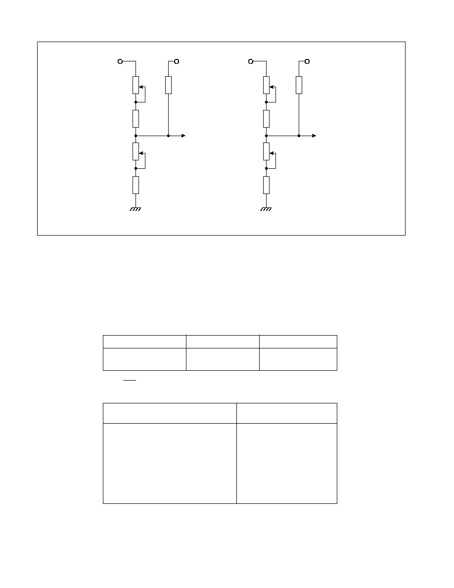
ANALOG INPUT RANGES
The basic connection of the ZN448/9 shown in Fig.15 has an
analogue input range 0 to V
REF IN
which, in some applications,
may be made available from previous signal conditioning/
scaling circuits. Input voltage ranges greater than this are
accommodated by providing an attenuator on the comparator
input, whilst for smaller input ranges the signal must be
amplified to a suitable level.
Bipolar input ranges are accommodated by off-setting the
analogue input input range so that the comparator always
sees a positive input voltage.
Fig.15 External components for basic operation
LSB
DB0
MSB
DB7
VCC
(+5V)
BUSY
1
18
1
RD
2
17
2
CK
3
16
3
WR
4
15
4
V-
(-5V)
5
14
5
AIN
6
13
6
VREFIN
7
12
VREFOUT
8
11
GND
(0V)
9
10
RREF
(390
)
REXT
(82k)
RIN
(4k)
VIN
CREF
(4�7)
DIGITAL OUTPUTS
NOMINAL AIN RANGE = 0 TO VREFIN

ZN448/9
13
UNIPOLAR OPERATION
The general connection for unipolar operation is shown in
Fig.16.
The values of R
1
and R
2
are chosen so that V
IN
= V
REF IN
when
the analog input (A
IN
) is at full-scale.
The resulting full-scale range is given by:
A
IN
FS = 1 + , V
REF IN
= G.V
REF IN
.
To match the ladder resistance R
1
/R
2
(R
IN
) = 4k.
The required nominal values of R
1
and R
2
are given by R
1
=
4Gk, R
2
= 4G k
G-1
Fig.16 General unipolar input connections
R1
R2
680k
1M
ZERO
ADJUST
GROUND
7
9
6
ZN448/9
VIN
AIN
VREF IN
Using these relationships a table of nominal values of R
1
and
R
2
can be constructed for V
REF IN
= 2.5V.
Gain adjustment
Due to tolerance in R
1
and R
2
, tolerance in V
REF
and the gain
(full-scale) error of the DAC, some adjustment should be
incorporated into R
1
to calibrate the full-scale of the converter.
When used with the internal reference and 2% resistors a
preset capable of adjusting R
1
by at least
�
5% of its nominal
value is suggested.
R
2
8k
5.33k
R
1
8k
16k
G
2
4
Input range
+5V
+10V
Zero adjustment
Due to offsets in the DAC and comparator the zero (0 to 1)
code transition would occur with typically 15mV applied to the
comparator input, which correpsonds to 1.5LSB with a 2.56V
reference.
Zero adjustment must therefore be provided to set the zero
transition to its correct value of +0.5LSB or 5mV with a 2.56V
reference. This is achieved by applying an adjustable positive
offset to the comparator input via P2 and R3. The values
shown are suitable for all input ranges greater than 1.5 times
V
REF IN
.
Practical circuit values for +5 and +10V input ranges are given
in Fig.17, which incorporates both zero and gain adjustments.
R
1
R
2

ZN448/9
14
Fig.17 Unipolar operation component values
AIN
VREF IN
TO PIN 6
R1 11k
R2 5k6
680k
R3
P2
P1 10k
GAIN
ADJUST
1M
ZERO
ADJUST
� 2% RESISTORS
�20% POTENTIOMETERS
AIN
VREF IN
TO PIN 6
R1 5k6
R2 8k2
680k
R3
P2
P1 5k
GAIN
ADJUST
1M
ZERO
ADJUST
+5V FULL-SCALE
+10V FULL-SCALE
Unipolar adjustment prodedure
(i) Apply continuous convert pulses at intervals long enough
to allow a complete conversion and monitor the digital
outputs.
(ii) Apply full-scale minus 1.5LSB to A
IN
and adjust off-set until
the bit 8 (LSB) output just flickers between 0 and 1 with all
other bits at 0.
(iii) Apply 0.5LSB to A
IN
and adjust zero until 8 bit just flickers
between 0 and 1 with all other bits at 1.
Unipolar setting up points
FS - 1.5LSB
4.9707V
9.9414V
1LSB = FS
256
Input range, +FS
+5V
+10V
0.5LSB
9.8mV
19.5mV
Bipolar logic coding
Analogue input (A
IN
)
(Nominal code centre value)
FS - 1LSB
FS - 2LSB
0.75FS
0.5FS + 1LSB
0.5FS
0.5FS - 1LSB
0.25FS
1LSB
0
Output code
(offset binary)
11111111
11111110
11000000
10000001
10000000
01111111
01000000
00000001
00000000

ZN448/9
15
BIPOLAR OPERATION
For bipolar operation the input to the ZN448/9 is offset by half
full-scale by connecting a resistor R
3
between V
REF IN
and V
IN
(Fig.18).
Fig.18 Basic bipolar input connection
R1
R3
R2
GROUND
7
9
6
ZN448/9
VIN
AIN
VREF IN
When A
IN
= -FS, V
IN
needs to be equal to zero.
When A
IN
= +FS, V
IN
needs to be equal to V
REF IN
.
If the full-scale range is
�
G. V
REF IN
then R
1
= (G - 1). R
2
and
R
1
= G. R
3
fulfil the required conditions.
To match the ladder resistance, R
1
/R
2
/R
3
(=R
IN
) = 4k.
Thus the nominal values of R
1
, R
2
, R
3
are given by R
1
= 8 Gk,
R
2
= 8G/(G - 1)k, R
3
= 8k.
A bipolar range of
�
V
REF IN
(which corresponds to the basic
unipolar range 0 to +V
REF IN
) results if R
1
= R
3
= 8k and R
2
=
.
Assuming the V
REF IN
= 2.5V the nominal values of resistors for
�
5 and
�
10V input ranges are given in the following table.
R
2
16k
10.66k
R
1
16k
32k
G
2
4
Input range
+5V
+10V
Minus full-scale (offset) is set by adjusting R
1
about its nominal
value relative to R
3
. Plus full-scale (gain) is set by adjusting R
2
relative to R
1
.
Practical circuit realisations are given in Fig.19.
R
3
8k
8k
Note that in the
�
5V case R
3
has been chosen as 7.5k (instead
of 8.2k) to obtain a more symmetrical range of adjustment
using standard potentiometers.
ZN448/9
16
Fig.19 Bipolar operation component values
AIN
VREF
TO PIN 6
13k
7k5
5k
OFFSET
ADJUST
13k
5k
GAIN
ADJUST
� 2% RESISTORS
�20% POTENTIOMETERS
�5VOLTS FULL SCALE
AIN
VREF
TO PIN 6
27k
8k2
10k
OFFSET
ADJUST
8k2
5k
GAIN
ADJUST
�10VOLTS FULL SCALE
Bipolar adjustment prodedure
(i) Apply continuous SC pulses at intervals long enough to
allow a complete conversion and monitor the digital
outputs.
(ii) Apply -(FS -0.5LSB) to A
IN
and adjust off-set until the bit 8
(LSB) output just flickers between 0 and 1 with all other bits
at 0.
(iii) Apply +(FS -1.5LSB) to A
IN
and adjust gain until the 8 bit
just flickers between 0 and 1 with all other bits at 1.
(iv) Repeat step (ii).
Bipolar setting up points
+(FS -1.5LSB)
+4.9414V
+9.8828V
1LSB =2FS
256
Input range,
�
FS
+5V
+10V
-(FS -0.5LSB)
-4.9805V
-9.9609V
Bipolar logic coding
Analogue input (A
IN
)
(Nominal code centre value)
+(FS - 1LSB)
+(FS - 2LSB)
+0.5FS
+1LSB
0
-1LSB
-0.5FS
-(FS - 1LSB)
-FS
Output code
(offset binary)
11111111
11111110
11000000
10000001
10000000
01111111
01000000
00000001
00000000

ZN448/9
17

www.zarlink.com
Information relating to products and services furnished herein by Zarlink Semiconductor Inc. trading as Zarlink Semiconductor or its subsidiaries (collectively
"
Zarlink
"
)
is believed to be reliable. However, Zarlink assumes no liability for errors that may appear in this publication, or for liability otherwise arising from the application or
use of any such information, product or service or for any infringement of patents or other intellectual property rights owned by third parties which may result from
such application or use. Neither the supply of such information or purchase of product or service conveys any license, either express or implied, under patents or
other intellectual property rights owned by Zarlink or licensed from third parties by Zarlink, whatsoever. Purchasers of products are also hereby notified that the use
of product in certain ways or in combination with Zarlink, or non-Zarlink furnished goods or services may infringe patents or other intellectual property rights owned
by Zarlink.
This publication is issued to provide information only and (unless agreed by Zarlink in writing) may not be used, applied or reproduced for any purpose nor form part
of any order or contract nor to be regarded as a representation relating to the products or services concerned. The products, their specifications, services and other
information appearing in this publication are subject to change by Zarlink without notice. No warranty or guarantee express or implied is made regarding the capability,
performance or suitability of any product or service. Information concerning possible methods of use is provided as a guide only and does not constitute any guarantee
that such methods of use will be satisfactory in a specific piece of equipment. It is the user
'
s responsibility to fully determine the performance and suitability of any
equipment using such information and to ensure that any publication or data used is up to date and has not been superseded. Manufacturing does not necessarily
include testing of all functions or parameters. These products are not suitable for use in any medical products whose failure to perform may result in significant injury
or death to the user. All products and materials are sold and services provided subject to Zarlink
'
s conditions of sale which are available on request.
Purchase of Zarlink s I
2
C components conveys a licence under the Philips I
2
C Patent rights to use these components in and I
2
C System, provided
that the system conforms to the I
2
C Standard Specification as defined by Philips.
Zarlink and the Zarlink Semiconductor logo are trademarks of Zarlink Semiconductor Inc.
Copyright 2001, Zarlink Semiconductor Inc. All Rights Reserved.
TECHNICAL DOCUMENTATION - NOT FOR RESALE
For more information about all Zarlink products
visit our Web Site at