 | –≠–ª–µ–∫—Ç—Ä–æ–Ω–Ω—ã–π –∫–æ–º–ø–æ–Ω–µ–Ω—Ç: ZN459 | –°–∫–∞—á–∞—Ç—å:  PDF PDF  ZIP ZIP |

ZN459, ZN459CP
ULTRA LOW NOISE WIDEBAND PREAMPLIFIER
Fig.1 ZN459 Outline circuit
A versatile high grade a.c. pre-amplifier designed for
applications requiring ultra low noise such as infra-red
imaging and low noise wide band amplifiers e.g. microphone,
acoustic emission, transducer bridge amplifier. The matching
of open loop gain coupled with small physical size make the
ZN459 series ideal for multichannel amplification.
FEATURES
s
High Controlled Gain
:
60dB
±
1dB typical
s
Low Noise
:
40
Equivalent Noise
Resistance, or 800pV/
H
z
s
Wide bandwidth
:
15MHz typical
s
Low Supply Current
:
<3mA from 5V
ABSOLUTE MAXIMUM RATINGS
Supply voltage
6 Volts
Operating Temperature Range:
for ZN459
-55 to +125
∞
C
for ZN459CP
0 to +70
∞
C
Storage Temperature Range
-55 to +125
∞
C
CM6
ZN459
DP8
ZN459CP
DS3623 - 2.0
ADVANCE INFORMATION

ZN459
Parameter
Min.
Typ.
Max.
Units
Conditions
Supply Current
2.0
2.5
3.0
mA
Voltage Gain
59
60
61
dB
10KHz
TC of Voltage Gain
-0.2
%/
∞
C
V
CC
Coefficient of Voltage Gain
25
%/V
Cut-off Frequency
15
MHz
3dB down
Input Resistance
3.5
7
k
10KHz
Input Capacitance
80
pF
Note 1
Noise Resistance
40
R
S
= 0
White Noise Voltage
800
1100 pV/
H
Z
R
S
= 0
L.F. Spot Noise
3
nV/
H
Z
R
S
= 0, f = 25Hz
White Noise Current
1
pA/
H
Z
Output Level
1.5
2.0
2.5
V
Supply Voltage Coefficient
of Output Level
0.34
V/V
Output Current Limit
0.6
0.8
1.1
mA
Sink current
Total Harmonic Distortion
0.15
%
1 Vpp at 10KHz
Output Resistance
75
10KHz
Supply Rejection Ratio
42.5
dB
Delay Time
20
ns
Small signal
Delay Time
40
ns
100mV rms input
Positive Input Overdrive
10
mA
Negative Input Overdrive
-5
V
ELECTRICAL CHARACTERISTICS
Test condltions (unless otherwise stated):
(V
CC
= 5V, T
amb
= 25
∞
C)
Note 1:
In P.C.B. The input capacitance may be reduced to 25pF by screening between output and input.
Fig.2 Pinning configuration - ZN459
Fig.3 Pinning configuration - ZN459CP

ZN459
Fig.4 Gain Test Circuit (ZN459)
The input impedance may be increased at the expense of
noise by including R
1
to vary the gain (R
1
= 0, gain = 10
3
; R
1
=
470
, gain = 10
2
).
C
d
is required to decouple the internal feedback loop and in
order to obtain a flat frequency response make C
d
> C
c
.
The earth lead of the supply decoupling capacitor should be as
close as possible to that of R
1
.
For optimum Common Mode Rejection connect a twisted pair
between source and pins 4 and 5 of the device and complete
the earth return from source ground.
Fig.5 ZN459 Input and output circuit
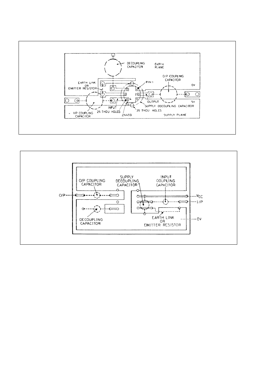
ZN459
Fig.6 PCB layout (ZN459)
Fig.7 PCB layout (ZN459CP)

ZN459
TYPICAL CHARACTERISTICS
Fig.8 Gain V
S
Frequency
Fig.9 Gain and noise resistance V
S
emitter resistance

ZN459
Fig.10 Gain and Input Impedance
Fig.11 Common Mode Rejection Vs Frequency
(Measured between input earth and output earth)

ZN459
Fig.12 Supply Current and Output Sink Current
Fig.13 Noise Voltage

ZN459
Fig.14 Quiescent Output Level