 | –≠–ª–µ–∫—Ç—Ä–æ–Ω–Ω—ã–π –∫–æ–º–ø–æ–Ω–µ–Ω—Ç: ZR2431G02 | –°–∫–∞—á–∞—Ç—å:  PDF PDF  ZIP ZIP |

SCHEMATIC DIAGRAM
DEVICE DESCRIPTION
The ZR2431 is a three terminal adjustable
s h u n t r e g u l a t o r o f f e r i n g e x c e l l e n t
temperature stability and output current
handling capability up to 25mA. The output
voltage may be set to any chosen voltage
between 1.24 and 15 volts by selection of
two external divider resistors.
The devices can be used as a replacement
for zener diodes in many applications
r e q u i r i n g a n i m p r o v e me n t i n z e n e r
performance.
The ZR2431 is particularly used in the
feedback control loop of switch mode power
supplies. In this application the device 1.24
volt reference enables the generation of low
voltage supplies, typically 3.3 volts or 3 volts.
FEATURES
∑
Surface mount SOT23, SOT223, SOT89
and SO8 packages
∑
TO92 package
∑
2.5% and 1% tolerance
∑
Maximum temperature coefficient 52
ppm/∞C
∑
Temperature compensated for
operation over the full temperature
range
∑
Programmable output voltage
∑
100
µ
A to 25mA current sink capability
∑
Low output noise
APPLICATIONS
∑
Shunt regulator
∑
Series regulator
∑
Voltage monitor
∑
Over voltage/ under voltage protection
∑
Switch mode power supplies
ADJUSTABLE PRECISION
ZENER SHUNT REGULATOR
ISSUE 3 DECEMBER 1997
ZR2431
V
Z
G
nd
V
ref
4-154

ZR2431
ABSOLUTE MAXIMUM RATING
Cathode Voltage (V
Z
)
15V
Cathode Current
50mA
Operating Temperature
-40 to 85∞C
Storage Temperature
-55 to 125∞C
Recommended Operating Conditions
Min
Max
Cathode Voltage
V
REF
15V
Cathode Current
100
µ
A 25mA
Power Dissipation (T
amb
=25∞C,
T
jmax
=150∞C)
SOT23
330mW
SOT223
2W
SO8
780mW
TO92
780mW
SOT89
1.5W
ELECTRICAL CHARACTERISTICS
TEST CONDITIONS (Unless otherwise stated):T
amb
=25∞C
PARAMETER
SYMBOL
VALUE
UNITS CONDITIONS
MIN
TYP MAX
Reference Voltage 2.5%
1.0%
V
ref
1.209
1.228
1.24
1.24
1.271
1.252
V
I
L
=10mA (Fig1), V
Z
=V
ref
Deviation of Reference Input
Voltage over Temperature
V
dev
4.0
8.0
mV
I
L
=10mA, V
Z
=V
ref
T
a
=full range (Fig1)
Ratio of the change in
Reference Voltage to the
Change in Cathode Voltage
V
ref
V
Z
0.5
2.0
mV/V
V
Z
from V
ref
to 10V
I
Z
=10mA (Fig2)
Reference Input Current
I
ref
0.02
0.11 0.4
µ
A
R1=10k, R2=O/C, l
L
=10mA (Fig2)
Deviation of Reference Input
Current over Temperature
I
ref
0.02 0.2
µ
A
R1=10k, R2=O/C, I
L
=10mA
T
a
=full range (Fig2)
Minimum Cathode
Current for Regulation
I
Zmin
30
100
µ
A
Off-state Current
I
Zoff
10
30
µ
A
V
Z
=15V, V
ref
=0V (Fig3)
Dynamic Output Impedance R
Z
0.25 2
V
Z
=V
ref
(Fig1), f=0Hz, I
L
=10mA
Deviation of reference input voltage, V
dev,
is defined as the maximum variation of the
reference input voltage over the full temperature range.
The average temperature coefficient of the
reference input voltage, V
ref
is defined as:
V
ref
(
ppm
/
∞
C
)=
V
dev
x 1000000
V
ref
(
T
1
-
T
2
)
The dynamic output impedance, Rz, is
defined as:
R
Z
=
V
Z
I
Z
When the device is programmed with two
external resistors, R1 and R2, (fig 2) , the
dynamic output impedance of the overall
circuit, R', is defined as:
R
'
=
R
z
(
1
+
R1
R2
)
With a capacitance of greater than 100pF
between cathode and anode, minimum
cathode current must be 0.2mA.
Vmax
Vmin
T1
T2
Vdev = Vmax - Vmin
Temperature
4-155
ZR2431
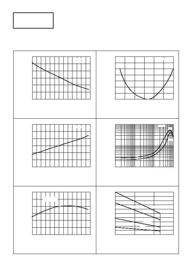
Reference Current v Temperature
Temperature (∞C)
0
20
60
40
80
R
e
f
e
r
e
n
c
e
C
u
r
r
en
t
(nA)
90
140
130
120
110
100
-40
-20
80
Dynamic Impedance v Frequency
Frequency (Hz)
1k
10k
100k
0.1
Dy
na
m
i
c I
m
pe
da
n
c
e
(
)
10
1
100
Change in V
ref
v Cathode Voltage
Cathode Voltage (V)
5
15
10
C
h
a
nge
i
n
R
e
fer
e
n
c
e
Outpu
t
V
o
l
t
a
g
e
(
m
V
)
-5
1
0
-1
-2
-3
0
2
-4
Cathode Current v Temperature
Temperature (∞C)
0
20
60
40
14
M
i
n
i
m
u
m
C
a
thode
C
u
r
r
e
nt(µA)
16
26
24
22
20
18
-40
-20
80
Reference Voltage v Temperature
Temperature (∞C)
0
20
60
40
R
e
f
e
r
e
nc
e
V
o
lta
ge
(V
)
1.240
1.236
-40
-20
80
1.234
1.232
1.238
1.242
1.244
Power Dissipation Derating
Ambient Temprature (∞C)
50
100
75
Pow
e
r
D
i
s
s
i
p
a
t
i
on (W
)
0
1.0
25
2.0
85
Vref = Vz
Iz=10mA
1mA
10mA
Vref = Vz
Iz = 10mA
Vref = Vz
SOT 223
SO8/TO92
SOT23
SOT 89
TYPICAL CHARACTERISTICS
TYPICAL CHARACTERISTICS
Iz=10mA
TYPICAL CHARACTERISTICS
4-156
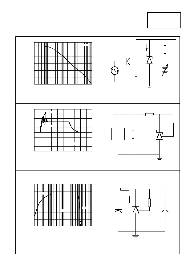
Stablity Boundary Conditions
Load Capacitance(F)
1n
10n
1µ
0
Cathod
e
Cu
r
r
e
nt(
m
A
)
5
30
25
20
15
10
10p
100p
.1µ
10µ
Pulse Response
Time (us)
200
300
500
400
V
o
l
tage S
w
i
n
g (V
)
0
2.0
1.0
0
5.0
2.5
0
100
Gain v Frequency
Frequency (Hz)
10k
100k
1M
0
Open Loop V
o
ltage
G
ain (dB)
10
60
50
40
30
20
100
1k
STABLE
STABLE
UNSTABLE
INPUT
Single
Pulse
Repetitive
Pulse
Vz
Iz = 10mA
TYPICAL CHARACTERISTICS
I
Z
47k
V
Z
Test Circuit for Open Loop Voltage Gain
47k
10
µ
F
240
+
-
I
Z
= 10mA,
T
A
= 25∞C
Test Circuit for Pulse Response
Input Monitor
V
Z
120
50
Pulse
Generator
T
A
= 25∞C
Test Circuit for Stability
Boundary Conditions
Input
150
10k
V
ref
< V
Z
< 20, I
Z
= 10mA, T
A
= 25∞C
V
Z
I
Z
100µF
ZR2431
4-157
ZR2431
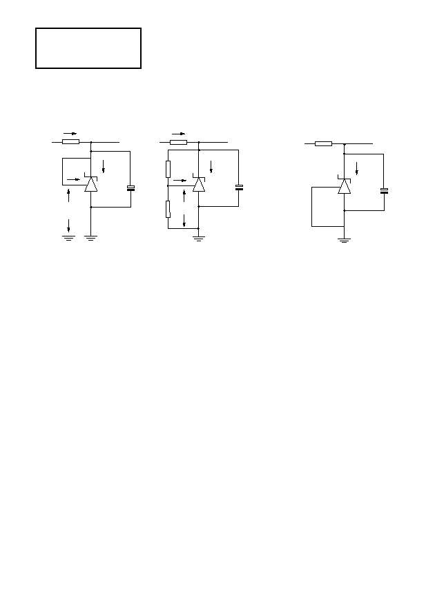
Input
V
V
I
Z
Z
ref
I
L
I
ref
1
µ
F
Fig 1 ≠ Test Circuit for V
z
=V
ref
DC TEST CIRCUITS
Input
V
V
I
Z
Z
ref
I
ref
R1
R2
I
L
1
µ
F
Fig 2 ≠ Test Circuit for V
z
>V
ref
Input
V
I
Z
zoff
1
µ
F
Fig 3 ≠ Test Circuit for Off
State current
4-158
ZR2431
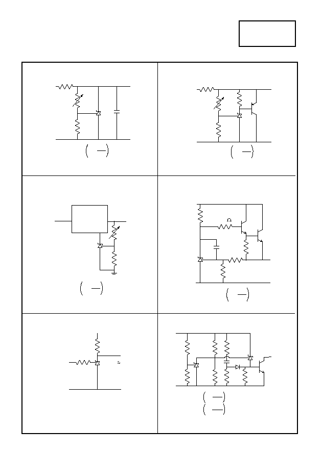
R2
Vout = 1 +
R1
R2
Vref
SERIES REGULATOR
V+
Vout
R1
30
0.01µF
Vref
Vout = 1 +
R1
R2
Vref
Vout = Vref + Vreg
MIN
OUTPUT CONTROL OF A
THREE TERMINAL FIXED REGULATOR
R2
R1
V+
Vout
Vref
ZSR***
In
Out
Common
R2
R1
V+
Vout
Vout =
Vref
1 +
R1
R2
Vref
HIGHER CURRENT SHUNT REGULATOR
V+
OUTPUT
INPUT
V
= 2.5V
TH
V
2V
on
V
= V+
off
SINGLE SUPPLY COMPARATOR
WITH TEMPERATURE
COMPENSATED THRESHOLD
R2A
R1A
V+
Vref
R2B
R1B
Vref
1 +
R1B
R2B
Vref
OVER VOLTAGE / UNDER VOLTAGE
PROTECTION CIRCUIT
Low limit =
High limit =
1 +
R1A
R2A
Vref
R2
R1
Vout =
Vref
1 +
R1
R2
Vref
SHUNT REGULATOR
V+
Vout
OUTPUT
APPLICATION CIRCUITS
4-159
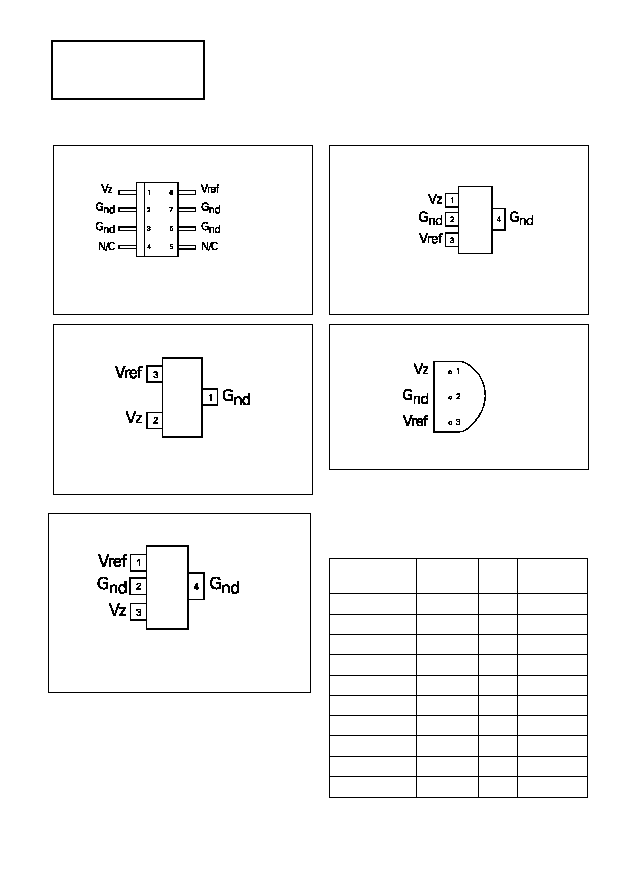
CONNECTION DIAGRAMS
ZR2431
SO8 Package Suffix ≠ N8
Top
View
SOT223 Package
Suffix ≠ G
Top
View ≠
Pin 4 floating or connected to pin 2
SOT23 Package
Suffix ≠ F
Top
View
TO92 Package Suffix ≠ C
Bottom
View
SOT89 Package
Suffix ≠ Z
Top
View
ORDERING INFORMATION
Part Number
Package
Tol
%
Part Mark
ZR2431N802
SO8
2.5
ZR243102
ZR2431N801
SO8
1
ZR243101
ZR2431G02
SOT223
2.5
ZR243102
ZR2431G01
SOT223
1
ZR243101
ZR2431F02
SOT23
2.5
24D
ZR2431F01
SOT23
1
24E
ZR2431Z02
SOT89
2.5
24D
ZR2431Z01
SOT89
1
24E
ZR2431C02
TO92
2.5
ZR243102
ZR2431C01
TO92
1
ZR243101
4-160