
MBD110≠1/5
1
3
2
Dual SCHOTTKY Barrier Diodes
MAXIMUM RATINGS
Rating
Symbol
Value
Unit
Reverse Voltage
MBD110DWT1
V
R
7.0
Vdc
MBD330DWT1
30
MBD770DWT1
70
Forward Power Dissipation
P
F
120
mW
T
A
= 25∞C
Junction Temperature
T
J
≠55 to +125
∞C
Storage Temperature Range
T
stg
≠55 to +150
∞C
DEVICE MARKING
MBD110DWT1 = M4 MBD330DWT1 = T4 MBD770DWT1 = H5
Thermal Clad is a trademark of the Bergquist Company.
6
4
5
SOT≠363
CASE 419B≠01, STYLE 6
MBD110DWT1
MBD330DWT1
MBD770DWT1
Application circuit designs are moving toward the consolidation of
device count and into smaller packages. The new SOT≠363 package is
a solution which simplifies circuit design, reduces device count, and
reduces board space by putting two discrete devices in one small six≠
leaded package. The SOT≠363 is ideal for low≠power surface mount
applications where board space is at a premium, such as portable
products.
1
2
3
Anode
N/C
Cathode
Cathode
N/C
Anode
6
5
4
Surface Mount Comparisons:
SOT≠363
SOT≠23
Area (mm
2
)
4.6
7.6
Max Package P
D
(mW)
120
225
Device Count
2
1
Space Savings:
Package
1 ◊ SOT≠23
2 ◊ SOT≠23
SOT≠363
40%
70%
The MBD110DW, MBD330DW, and MBD770DW devices are spin≠offs of our popular
MMBD101LT1, MMBD301LT1, and MMBD701LT1 SOT≠23 devices. They are designed
for high≠efficiency UHF and VHF detector applications. Readily available to many other
fast switching RF and digital applications.
∑ Extremely Low Minority Carrier Lifetime
∑ Very Low Capacitance
∑ Low Reverse Leakage

MBD110≠2/5
MBD110DWT1 MBD330DWT1 MBD770DWT1
ELECTRICAL CHARACTERISTICS
(T
A
= 25∞C unless otherwise noted)
Characteristic
Symbol
Min
Typ
Max
Unit
Reverse Breakdown Voltage
V
(BR)R
Volts
(I
R
= 10
µ
A)
MBD110DWT1
7.0
10
--
MBD330DWT1
30
--
--
MBD770DWT1
70
--
--
Diode Capacitance
C
T
pF
(V
R
= 0, f = 1.0 MHz, Note 1)
MBD110DWT1
--
0.88
1.0
Total Capacitance
C
T
pF
(V
R
= 15 Volts, f = 1.0 MHz)
MBD330DWT1
--
0.9
1.5
(V
R
= 20 Volts, f = 1.0 MHz)
MBD770DWT1
--
0.5
1.0
Reverse Leakage
I
R
(V
R
= 3.0 V)
MBD110DWT1
--
0.02
0.25
µ
A
(V
R
= 25 V)
MBD330DWT1
--
13
200
nAdc
(V
R
= 35 V)
MBD770DWT1
--
9.0
200
nAdc
Noise Figure
NF
dB
(f = 1.0 GHz, Note 2)
MBD110DWT1
--
6.0
--
Forward Voltage
V
F
Vdc
(I
F
= 10 mA)
MBD110DWT1
--
0.5
0.6
(I
F
= 1.0 mAdc)
MBD330DWT1
--
0.38
0.45
(I
F
= 10 mA)
--
0.52
0.6
(I
F
= 1.0 mAdc)
MBD770DWT1
--
0.42
0.5
(I
F
= 10 mA)
--
0.7
1.0

MBD110≠3/5
TYPICAL CHARACTERISTICS -- MBD110DWT1
MBD110DWT1 MBD330DWT1 MBD770DWT1
30
40
50
60
70
80
90
100
110
120
130
1.0
0.7
0.5
0.2
0.1
0.07
0.05
0.02
0.01
0.3
0.4
0.5
0.6
0.7
0.8
100
10
1.0
0.1
0
1.0
2.0
3.0
4.0
1.0
0.9
0.8
0.7
0.6
0.1
0.2
0.5
1.0
2.0
5.0
10
11
10
9
8
7
6
5
4
3
2
1
NF, NOISE FIGURE (dB)
C, CAP
ACIT
ANCE (pF)
I
R
, REVERSE LEAKAGE (
µ
A)
T
A
, AMBIENT TEMPERATURE (∞C)
Figure 1. Reverse Leakage
V
F
, FORWARD VOLTAGE (VOLTS)
Figure 2. Forward Voltage
I
F
, FOR
W
ARD CURRENT
(mA)
V
R
, REVERSE VOLTAGE (VOLTS)
Figure 3. Capacitance
P
LO
, LOCAL OSCILLATOR POWER (mW)
Figure 4. Noise Figure
Figure 5. Noise Figure Test Circuit
NOTES ON TESTING AND SPECIFICATIONS
Note 1 ≠ C
C
and C
T
are measured using a capaci-
tance bridge (Boonton Electronics Model 75A
or equivalent).
Note 2 ≠ Noise figure measured with diode under
test in tuned diode mount using UHF noise
source and local oscillator (LO) frequency of
1.0 GHz. The LO power is adjusted for 1.0
mW. I
F
amplifier NF = 1.5 dB, f = 30 MHz, see
Figure 5.
Note 3 ≠ L
S
is measured on a package having a
short instead of a die, using an impedance
bridge (Boonton Radio Model 250A RX Meter).
MBD110≠4/5
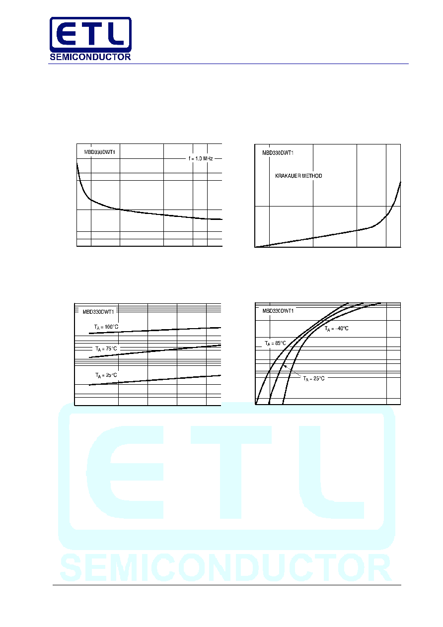
TYPICAL CHARACTERISTICS MBD330DWT1
MBD110DWT1 MBD330DWT1 MBD770DWT1
0
3.0
6.0
9.0
12
15
18
21
24
27
30
2.8
2.4
2.0
1.6
1.2
0.8
0.4
0
0
10
20
30
40
50
60
70
80
90
100
500
400
300
200
100
0
0
6.0
12
18
24
30
10
1.0
0.1
0.01
0.001
0.2
0.4
0.6
0.8
1.0
1.2
100
10
1.0
0.1
V
R
, REVERSE VOLTAGE (VOLTS)
Figure 6. Total Capacitance
I
F
, FORWARD CURRENT (mA)
Figure 7. Minority Carrier Lifetime
I
F
, FORW
ARD CURRENT
(mA)
, MINORITY CARRIER LIFETIME (ps)
C
T
,
T
O
T
A
L
CAP
ACIT
ANCE
(pF)
I
R
, REVERSE LEAKAGE (
µ
A)
V
R
, REVERSE VOLTAGE (VOLTS)
Figure 8. Reverse Leakage
V
F
, FORWARD VOLTAGE (VOLTS)
Figure 9. Forward Voltage
MBD110≠5/5
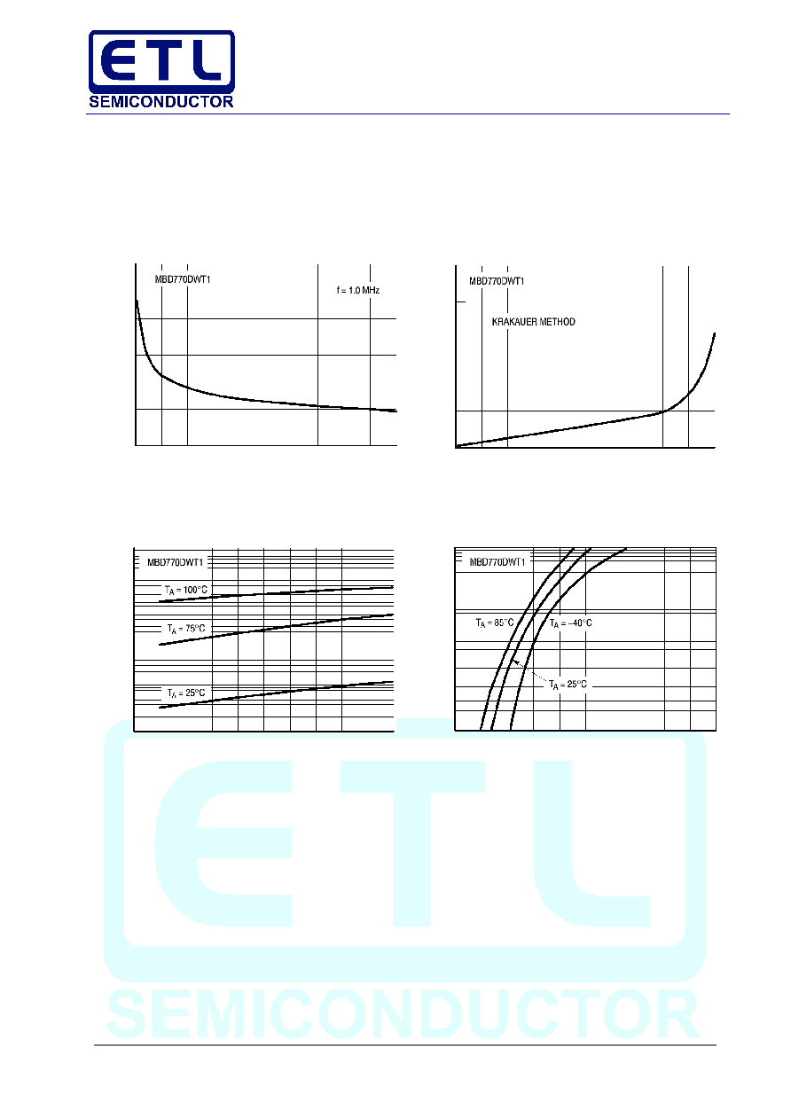
TYPICAL CHARACTERISTICS MBD770DWT1
MBD110DWT1 MBD330DWT1 MBD770DWT1
0
5.0
10
15
20
25
30
35
40
45
50
2.0
1.6
1.2
0.8
0.4
0
0
10
20
30
40
50
60
70
80
90
100
500
400
300
200
100
0
0
10
20
30
40
50
10
1.0
0.1
0.01
0.001
0.2
0.4
0.8
1.2
1.6
2.0
100
10
1.0
0.1
V
R
, REVERSE VOLTAGE (VOLTS)
Figure 10 . Total Capacitance
I
F
, FORWARD CURRENT (mA)
Figure 11. Minority Carrier Lifetime
I
F
, FORW
ARD CURRENT
(mA)
, MINORITY CARRIER LIFETIME (ps)
C
T
,
T
O
T
A
L
CAP
ACIT
ANCE
(pF)
I
R
, REVERSE LEAKAGE (
µ
A)
V
R
, REVERSE VOLTAGE (VOLTS)
Figure 12. Reverse Leakage
V
F
, FORWARD VOLTAGE (VOLTS)
Figure 13. Forward Voltage