VHT0≠1/4
VH
d
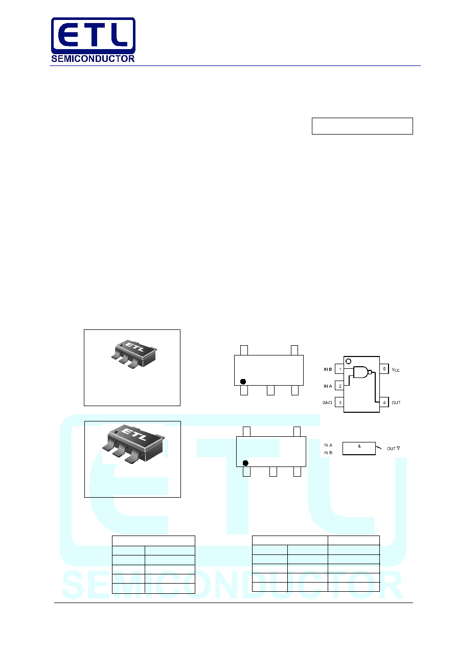
MC74VHC1GT00
VH
d
1
3
2
4
5
SOT≠23/TSOP≠5/SC≠59
DT SUFFIX
CASE 483
The MC74VHC1GT00 is a single gate 2≠input NAND fabricated with silicon gate CMOS technology. It achieves high speed operation
similar to equivalent Bipolar Schottky TTL while maintaining CMOS low power dissipation.
The internal circuit is composed of three stages, including a buffer output which provides high noise immunity and stable output.
The device input is compatible with TTL≠type input thresholds and the output has a full 5 V CMOS level output swing. The input
protection circuitry on this device allows overvoltage tolerance on the input, allowing the device to be used as a logic≠level translator from
3.0 V CMOS logic to 5.0 V CMOS Logic or from 1.8 V CMOS logic to 3.0 V CMOS Logic while operating at the high≠voltage power
supply.
The MC74VHC1GT00 input structure provides protection when voltages up to 7 V are applied, regardless of the supply voltage. This
allows the MC74VHC1GT00 to be used to interface 5 V circuits to 3 V circuits. The output structures also provide protection when
V
CC
= 0 V. These input and output structures help prevent device destruction caused by supply voltage ≠ input/output voltage mismatch,
battery backup, hot insertion, etc.
SC≠70/SC≠88A/SOT≠353
DF SUFFIX
CASE 419A
1
3
2
4
5
MARKING DIAGRAMS
Pin 1
d = Date Code
Pin 1
d = Date Code
Figure 1. Pinout (Top View)
Figure 2. Logic Symbol
PIN ASSIGNMENT
1
IN B
2
IN A
3
GND
4
OUT Y
5
V
CC
FUNCTION TABLE
Inputs
Output
A
B
Y
L
L
H
L
H
H
H
L
H
H
H
L
ORDERING INFORMATION
See detailed ordering and shipping information in the
package dimensions section on page 4 of this data sheet.
2≠Input NAND Gate / CMOS Logic Level Shifter
with LSTTL≠Compatible Inputs
∑
High Speed: t
PD
= 3.1 ns (Typ) at V
CC
= 5 V
∑
Low Power Dissipation: I
CC
=
2
mA (Max) at T
A
= 2
5∞
C
∑
TTL≠Compatible Inputs: V
IL
= 0.8 V; V
IH
= 2.0 V
∑
CMOS≠Compatible Outputs: V
OH
> 0.8 V
CC
; V
OL
< 0.1
V
CC
@Load
∑
Power Down Protection Provided on Inputs and Outputs
∑
Balanced Propagation Delays
∑
Pin and Function Compatible with Other Standard Logic
Families
∑
Chip Complexity: FETs = 64; Equivalent Gates = 14
Y

VHT0≠2/4
MC74VHC1GT00
RECOMMENDED OPERATING CONDITIONS
Symbol
Parameter
Min
Max
Unit
V
CC
DC Supply Voltage
3.0
5.5
V
V
IN
DC Input Voltage
0.0
5.5
V
V
OUT
DC Output Voltage
V
CC
=0
0.0
5.5
V
High or Low State
0.0
V
CC
T
A
Operating Temperature Range
≠ 55
+ 125
∞C
t
r
,t
f
Input Rise and Fall Time
V
CC
= 3.3 ± 0.3 V
0
100
ns/V
V
CC
= 5.0 ± 0.5 V
0
20
DEVICE JUNCTION TEMPERATURE VERSUS
TIME TO 0.1% BOND FAILURES
Junction
Time,
Time,
Temperature ∞C
Hours
Years
80
1,032,200
117.8
90
419,300
47.9
100
178,700
20.4
110
79,600
9.4
120
37,000
4.2
130
17,800
2.0
140
8,900
1.0
NORMALIZED F
AILURE RA
TE
Figure 3. Failure Rate vs. Time Junction Temperature
1
1
10
100
1000
MAXIMUM RATINGS
Symbol
Parameter
Value
Unit
V
CC
DC Supply Voltage
≠ 0.5 to + 7.0
V
V
IN
DC Input Voltage
≠ 0.5 to +7.0
V
V
OUT
DC Output Voltage
V
CC
=0
≠ 0.5 to +7.0
V
High or Low State
≠0.5 to V
cc
+ 0.5
I
IK
Input Diode Current
≠20
mA
I
OK
Output Diode Current
V
OUT
< GND; V
OUT
> V
CC
+20
mA
I
OUT
DC Output Current, per Pin
+ 25
mA
I
CC
DC Supply Current, V
CC
and GND
+50
mA
P
D
Power dissipation in still air
SC≠88A, TSOP≠5
200
mW
JA
Thermal resistance
SC≠88A, TSOP≠5
333
∞C/W
T
L
Lead Temperature, 1 mm from Case for 10 s
260
∞C
T
J
Junction Temperature Under Bias
+ 150
∞C
T
stg
Storage temperature
≠65 to +150
∞C
V
ESD
ESD Withstand Voltage
Human Body Model (Note 2)
>2000
V
Machine Model (Note 3)
> 200
Charged Device Model (Note 4)
N/A
I
LATCH≠UP
Latch≠Up Performance
Above V
CC
and Below GND at 125∞C (Note 5)
± 500
mA
1. Maximum Ratings are those values beyond which damage to the device may occur. Exposure to these conditions or conditions
beyond those indicated may adversely affect device reliability. Functional operation under absolute≠maximum≠rated conditions is
not implied. Functional operation should be restricted to the Recommended Operating Conditions.
2. Tested to EIA/JESD22≠A114≠A
3. Tested to EIA/JESD22≠A115≠A
4. Tested to JESD22≠C101≠A
5. Tested to EIA/JESD78
TIME, YEARS
VHT0≠3/4
DC ELECTRICAL CHARACTERISTICS
V
CC
T
A
= 25∞C
T
A
< 85∞C ≠55∞C to 125∞C
Symbol Parameter
Test Conditions
(V)
Min
Typ
Max
Min
Max
Min
Max
Unit
V
IH
Minimum High≠Level
V
Input Voltage
3.0
1.4
1.4
1.4
4.5
2.0
2.0
2.0
5.5
2.0
2.0
2.0
V
IL
Maximum Low≠Level
V
Input Voltage
3.0
0.53
0.53
0.53
4.5
0.8
0.8
0.8
5.5
0.8
0.8
0.8
V
OH
Minimum High≠Level
V
IN
= V
IH
or V
IL
V
Output Voltage
I
OH
= ≠ 50
µ
A
3.0
2.9
3.0
2.9
2.9
V
IN
= V
IH
or V
IL
4.5
4.4
4.0
4.4
4.4
V
IN
= V
IH
or V
IL
I
OH
= ≠4 mA
3.0
2.58
2.48
2.34
I
OH
= ≠8 mA
4.5
3.94
3.80
3.66
V
OL
Maximum Low≠Level
V
IN
= V
IH
or V
IL
V
Output Voltage
I
OL
= 50
µ
A
3.0
0.0
0.1
0.1
0.1
V
IN
= V
IH
or V
IL
4.5
0.0
0.1
0.1
0.1
V
IN
= V
IH
or V
IL
I
OL
= 4 mA
3.0
0.36
0.44
0.52
I
OL
= 8 mA
4.5
0.36
0.44
0.52
I
IN
Maximum Input
V
IN
= 5.5 V or GND
0 to5.5
±
0.1
±
1.0
±
1.0
µ
A
Leakage Current
I
CC
Maximum Quiescent
V
IN
= V
CC
or GND
5.5
2.0
20
40
µ
A
Supply Current
I
CCT
Quiescent Supply
Input: V
IN
= 3.4 V
5.5
1.35
1.50
1.65
mA
Current
I
OPD
Output Leakage
V
OUT
= 5.5 V
0.0
0.5
5.0
10
µ
A
Current
MC74VHC1GT00
AC ELECTRICAL CHARACTERISTICS C
load
= 50 pF, Input t
r
= t
f
= 3.0 ns
T
A
= 25∞C
T
A
< 85∞C ≠55∞C<T
A
<125∞C
Symbol Parameter
Test Conditions
Min
Typ
Max
Min
Max
Min
Max Unit
t
PLH
,
Maximum
V
CC
= 3.3
±
0.3 V
C
L
= 15 pF
4.1
10.0
11.0
13.0
ns
t
PHL
Propagation Delay,
C
L
= 50 pF
5.5
13.5
15.0
17.5
Input A or B to Y
V
CC
= 5.0
±
0.5 V C
L
= 15 pF
3.1
6.9
8.0
9.5
C
L
= 50 pF
3.6
7.9
9.0
10.5
C
IN
Maximum Input
5.5
10
10
10
pF
Capacitance
Typical @ 25∞C, V
CC
= 5.0 V
C
PD
Power Dissipation Capacitance (Note 6)
11
pF
6. C
PD
is defined as the value of the internal equivalent capacitance which is calculated from the operating current consumption without
load. Average operating current can be obtained by the equation: I
CC(OPR)
= C
PD
∑
V
CC
∑
f
in
+ I
CC
.
C
PD
is used to determine the no≠
load dynamic power consumption; P
D
= C
PD
∑
V
CC
2
∑
f
in
+ I
CC
∑
V
CC
.
VHT0≠4/4
DEVICE ORDERING INFORMATION
MC74VHC1GT00
Device Nomenclature
Device Order
Number
Logic
Circuit
Indicator
Temp
Range
Identifier
Technology
Device
Function
Package
Suffix
Tape and
Reel Suffix
Package Type
(Name/SOT#/
Common Name)
Tape and
Reel Size
MC74VHC1GT00DFT1
MC
74
VHC1G
T00
DF
T1
SC≠70/SC≠88A/
178 mm (7 in)
SOT≠353
3000 Unit
MC74VHC1GY00DFT2
MC
74
VHC1G
T00
DF
T2
SC≠70/SC≠88A/
178 mm (7 in)
SOT≠353
3000 Unit
MC74VHC1GT00DFT4
MC
74
VHC1G
T00
DF
T4
SC≠70/SC≠88A/
330 mm (13 in)
SOT≠353
10,000 Unit
MC74VHC1GT00DTT1
MC
74
VHC1G
T00
DT
T1
SOT≠23/TSOPS/
178 mm (7 in)
SC≠59
3000 Unit
MC74VHC1GT00DTT3
MC
74
VHC1G
T00
DT
T3
SOT≠23/TSOPS/
330 mm (13 in)
SC≠59
10,000 Unit
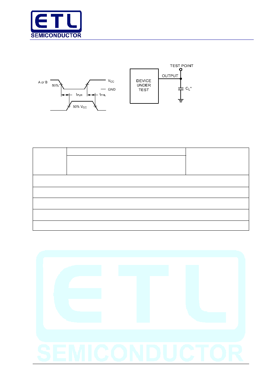
Figure 4. Switching Waveforms
Figure 5. Test Circuit
*Includes all probe and jig capacitance.
A 1≠MHz square input wave is recommended
for propagation delay tests.
Y