VHT66≠1/6
The MC74VHC1GT66 is an advanced high speed CMOS bilateral analog switch fabricated with silicon gate CMOS technology. It
achieves high speed propagation delays and low ON resistances while maintaining low power dissipation. This bilateral switch controls
analog and digital voltages that may vary across the full power≠supply range (from VCC to GND).
The MC74VHC1GT66 is compatible in function to a single gate of the very High Speed CMOS MC74VHCT4066. The device has
been designed so that the ON resistances (RON) are much lower and more linear over input voltage.
The ON/OFF Control input is compatible with TTL≠type input thresholds allowing the device to be used as a logic≠level translator from
3.0 V CMOS logic to 5.0 V CMOS logic or from 1.8 V CMOS logic to 3.0 V CMOS logic while operating at the high≠voltage power supply.
The input protection circuitry on this device allows overvoltage tolerance on the input, which provides protection when voltages of up to 7
V are applied, regardless of the supply voltage. This allows the MC74VHC1GT66 to be used to interface 5 V circuits to 3 V circuits.
∑ High Speed: t
PD
= 20 ns (Typ) at V
CC
= 5 V
∑ Low Power Dissipation: I
CC
= 2
µ
A (Max) at T
A
= 25∞C
∑ Diode Protection Provided on Inputs and Outputs
∑ Improved Linearity and Lower ON Resistance over Input Voltage
∑ On/Off Control Input Has OVT
ANALOG Switch
VE
d
VE
d
1
3
2
4
5
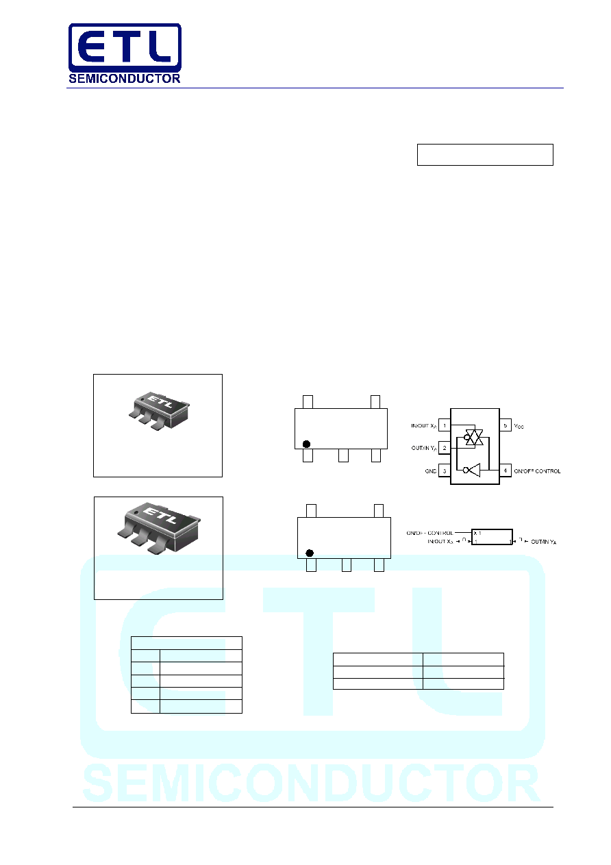
SOT≠23/TSOP≠5/SC≠59
DT SUFFIX
CASE 483
SC≠70/SC≠88A/SOT≠353
DF SUFFIX
CASE 419A
1
3
2
4
5
MARKING DIAGRAMS
Pin 1
d = Date Code
Pin 1
d = Date Code
Figure 1. Pinout (Top View)
Figure 2. Logic Symbol
PIN ASSIGNMENT
1
IN/OUT X
A
2
OUT/IN Y
A
3
GND
4
ON/OFF CONTROL
5
V
CC
FUNCTION TABLE
On / Off Control Input State Analog Switch
L
Off
H
On
ORDERING INFORMATION
See detailed ordering and shipping information in the
package dimensions section on page 6 of this data sheet.
MC74VHC1GT66

VHT66≠2/6
MC74VHC1GT66
MAXIMUM RATINGS
Symbol
Parameter
Value
Unit
V
CC
DC Supply Voltage
≠ 0.5 to + 7.0
V
V
IN
DC Input Voltage
≠ 0.5 to +7.0
V
V
IS
Analog Output Voltage
≠0.5 to +7.0
V
I
IK
Input Diode Current
≠20
mA
I
CC
DC Supply Current, V
CC
and GND
+25
mA
P
D
Power dissipation in still air
SC≠88A (Note 2.)
200
mW
TSOP5 (Note 2.)
450
T
L
Lead Temperature, 1 mm from Case for 10 s
260
∞C
T
stg
Storage temperature
≠65 to +150
∞C
V
ESD
ESD Withstand Voltage
Human Body Model (Note 3)
>2000
V
Machine Model (Note 4)
> 200
Charged Device Model (Note 5)
N/A
I
LATCH≠UP
Latch≠Up Performance
Above V
CC
and Below GND at 125∞C (Note 6)
± 500
mA
1. Maximum Ratings are those values beyond which damage to the device may occur. Exposure to these conditions or conditions
eyond those indicated may adversely affect device reliability. Functional operation under absolute≠maximum≠rated conditions is not
implied. Functional operation should be restricted to the Recommended Operating Conditions.
2. Derating ≠ SC≠88A Package: ≠3 mW/∞C from 65∞C
to 125∞C
≠ TSOP5 Package: ≠6 mW/∞C from 65∞C
to 125∞C
3. Tested to EIA/JESD22≠A114≠A
4. Tested to EIA/JESD22≠A115≠A
5. Tested to JESD22≠C101≠A
6. Tested to EIA/JESD78
DEVICE JUNCTION TEMPERATURE VERSUS
TIME TO 0.1% BOND FAILURES
Junction
Time,
Time,
Temperature ∞C
Hours
Years
80
1,032,200
117.8
90
419,300
47.9
100
178,700
20.4
110
79,600
9.4
120
37,000
4.2
130
17,800
2.0
140
8,900
1.0
NORMALIZED F
AILURE RA
TE
Figure 3. Failure Rate vs. Time Junction Temperature
1
1
10
100
1000
TIME, YEARS
RECOMMENDED OPERATING CONDITIONS
Symbol
Parameter
Min
Max
Unit
V
CC
DC Supply Voltage
2.0
5.5
V
V
IN
DC Input Voltage
GND
5.5
V
V
IS
Analog Input Voltage
GND
V
CC
V
T
A
Operating Temperature Range
≠ 55
+ 125
∞C
t
r
,t
f
Input Rise and Fall Time
V
CC
= 3.3 ± 0.3 V
0
100
ns/V
V
CC
= 5.0 ± 0.5 V
0
20
The
JA
of the package is equal to 1/Derating. Higher junction temperatures may affect the expected lifetime of the device per the
table and figure below.

VHT66≠3/6
MC74VHC1GT66
AC ELECTRICAL CHARACTERISTICS C
load
= 50 pF, Input t
r
/ t
f
= 3.0 ns
V
CC
T
A
= 25∞C
T
A
< 85∞C ≠55∞C<T
A
<125∞C
Symbol Parameter
Test Conditions
(V)
Min
Typ
Max
Min
Max
Min
Max Unit
DC ELECTRICAL CHARACTERISTICS
V
CC
T
A
= 25∞C
T
A
< 85∞C T
A
<125∞C
Symbol Parameter
Test Conditions
(V)
Min
Max
Min
Max
Min
Max
Unit
V
IH
Minimum High≠Level
R
ON
=Per Spec
V
Input Voltage
3.0
1.2
1.2
1.2
On/Off Control Input
4.5
2.0
2.0
2.0
5.5
2.0
2.0
2.0
V
IL
Maximum Low≠Level
R
ON
=Per Spec
V
Input Voltage
3.0
0.53
0.53
0.53
4.5
0.8
0.8
0.8
5.5
0.8
0.8
0.8
I
IN
Maximum Input
V
IN
=x V
cc
or GND 0 to 5.5
±
0.1
±
1.0
±
1.0
µ
A
Leakage Current
On/Off Control Input
I
CC
Maximum Quiescent
V
IN
= V
CC
or GND
5.5
2.0
20
40
µ
A
Supply Current
I
CCT
Quiescent Supply
On/Off Control
5.5
1.35
1.50
1.65
mA
Current
at 3.4 V
R
ON
Maximum "ON"
V
IN
= V
IH
3.0
60
70
100
Resistance
V
IS
= V
CC
or GND
4.5
45
50
60
|I
IS
|
<
10 mA (Figure 4.)
5.5
40
45
55
I
OFF
Maximum Off≠Channel
V
IN
= V
IL
5.5
0.1
0.5
1.0
mA
Leakage Current
V
IS
= V
CC
or GND
Switch Off (Figure 5.)
t
PLH
,
t
PHL
Maximum Propogation
Delay,
Input X to Y
Y
A
= Open
(Figure 14.)
2.0
3.0
4.5
5.5
1
0
0
0
5
2
1
1
6
3
1
1
7
4
2
1
ns
t
PLZ
,
t
PHZ
Maximum Propogation
Delay,
ON/OFF Control to
Analog Output
R
L
= 1000
(Figure 15.)
2.0
3.0
4.5
5.5
32
28
24
20
40
35
30
25
45
40
35
30
50
45
40
35
ns
t
PZL
,
t
PZH
Maximum Propogation
Delay,
ON/OFF Control to
Analog Output
R
L
= 1000
(Figure 15.)
2.0
3.0
4.5
5.5
32
28
24
20
40
35
30
25
45
40
35
30
50
45
40
35
ns
C
IN
Maximum Input
Capacitance
ON/OFF Control Input
0.0
3
10
10
10
pF
Contol Input = GND
Analog I/O
Feedthrough
5.0
4
4
10
10
10
10
10
10
7. C
PD
is defined as the value of the internal equivalent capacitance which is calculated from the operating current consumption without
load. Average operating current can be obtained by the equation: I
CC(OPR)
= C
PD
∑
V
CC
∑
f
in
+ I
CC
.
C
PD
is used to determine the no≠
load dynamic power consumption; P
D
= C
PD
∑ V
CC
2
∑
f
in
+ I
CC
∑
V
CC
.
Typical @ 25∞C, V
CC
= 5.0 V
C
PD
Power Dissipation Capacitance (Note 6)
18
pF

VHT66≠4/6
MC74VHC1GT66
BW
ADDITIONAL APPLICATION CHARACTERISTICS (Voltages Referenced to GND Unless Noted)
Symbol
Parameter
Test Conditions
V
CC
Limit
Unit
25∞C
Maximum On≠Channel Bandwidth
or Minimum Frequency Response
(Figure 10.)
f
in
= 1 MHz Sine Wave
Adjust f
in
voltage to obtain 0 dBm at V
OS
Increase f
in
= frequency until dB meter reads ≠3 dB
R
L
= 50
, C
L
= 10 pF
3.0
4.5
5.5
150
175
180
MHz
ISO
off
Off≠Channel Feedthrough
Isolation
(Figure 11.)
f
in
= Sine Wave
Adjust f
in
voltage to obtain 0 dBm at V
IS
f
in
= 10 kHz, R
L
= 600
, C
L
= 50 pF
3.0
4.5
5.5
≠80
≠80
≠80
dB
NOISE
feed
Feedthrough Noise Control to
Switch
(Figure 12.)
V
in
<1 MHz Square Wave (t
r
= t
f
= 2ns)
Adjust R
L
at setup so that I
s
= 0 A
R
L
= 600
, C
L
= 50 pF
3.0
4.5
5.5
45
60
130
mV
PP
THD
Total Harmonic Distortion
(Figure 13.)
f
in
= 1 kHz, R
L
= 10 k
, C
L
= 50 pF
THD = THD
Measured
≠ THD
Source
V
IS
= 3.0 V
PP
sine wave
V
IS
= 5.0 V
PP
sine wave
3.3
5.5
0.30
0.15
%
Figure 4. On Resistance Test Set≠Up
Figure 6. Maximum On≠Channel Leakage Current
Test Set≠Up
Figure 5. Maximum Off≠Channel Leakage Current
Test Set≠Up
Figure 7. Propagation Delay Test Set≠Up

VHT66≠5/6
MC74VHC1GT66
Switch to Position 1 when testing t
PLZ
and t
PZL
Switch to Position 2 when testing t
PHZ
and t
PZH
Figure 8. Propagation Delay Output Enable/Disable
Test Set≠Up
Figure 10. Maximum On≠Channel Bandwidth
Test Set≠Up
Figure 12. Feedthrough Noise, ON/OFF Control to
Analog Out, Test Set≠Up
Figure 9. Power Dissipation Capacitance
Test Set≠Up
Figure 11. Off≠Channel Feedthrough Isolation
Test Set≠Up
Figure 13. Total Harmonic Distortion Test
Set≠Up