EtronTech
EM562081
Etron Technology, Inc.
No. 6, Technology Rd. V, Science-Based Industrial Park, Hsinchu, Taiwan 30077, R.O.C
TEL: (886)-3-5782345
FAX: (886)-3-5778671
Etron Technology, Inc., reserves the right to make changes to its products and specifications without notice.
256K x 8 Low Power SRAM
Preliminary, Rev 1.0 7/2001
Features
∑
Single power supply voltage of 2.7V to 3.6V
∑
Power down features using CE1# and CE2
∑
Low operating current : 25mA(max. for 70 ns)
∑
Maximum Standby current : 10
µ
A
at 3.6 V
∑
Data retention supply voltage: 1.5V to 3.6V
∑
Direct TTL compatibility for all input and output
∑
Wide operating temperature range: -40
∞
C to 85
∞
C
∑
Package type: 36-ball TFBGA, 6x8mm
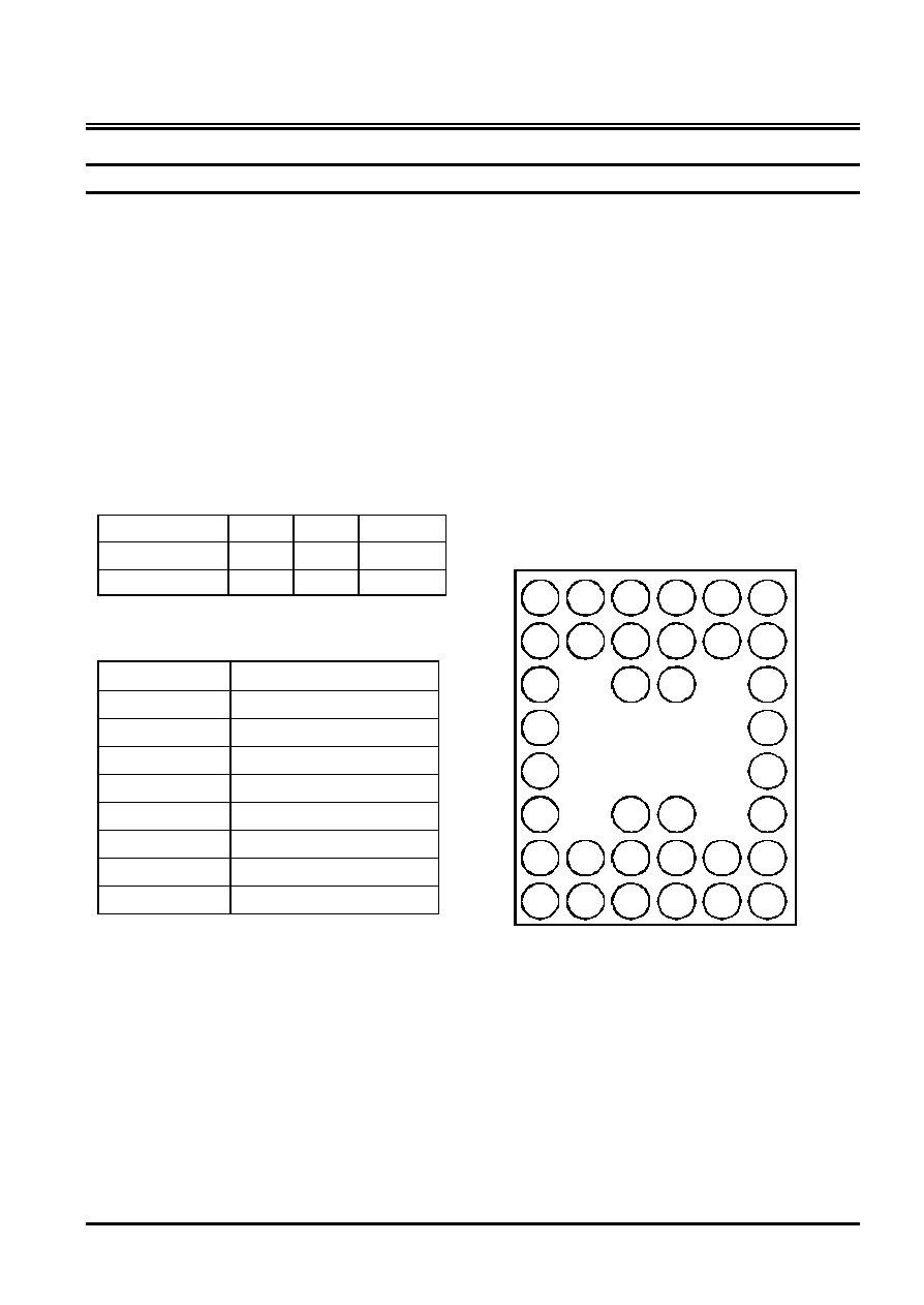
Ordering Information
Part Number
Speed I
DDS2
Package
EM562081BC-70
70 ns
10
µ
A
6x8 BGA
EM562081BC-85
85 ns
10
µ
A
6x8 BGA
Pin Names
Symbol
Function
A0 - A17
Address Inputs
DQ0-DQ7
Data Inputs/Outputs
CE1#,CE2
Chip Enable Inputs
OE#
Output Enable
WE#
Read/Write Control Input
GND
Ground
VDD
Power Supply
NC
No Connection
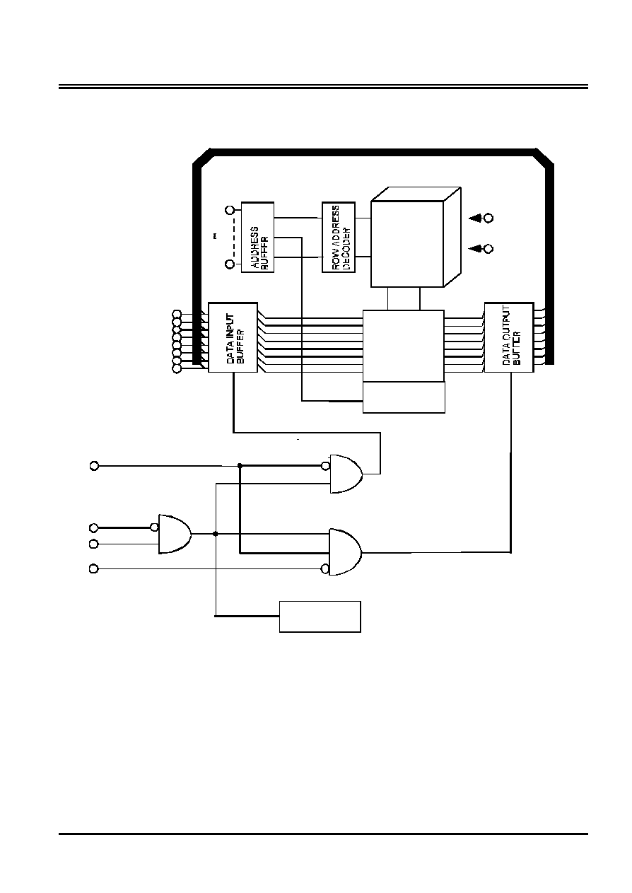
asserted low. There are three control inputs. CE1# and
CE2 are used to select the device and for data retention
control, and output enable (OE#) provides fast memory
access. Data byte control pin (LB#,UB#) provides lower
and upper byte access. This device is well suited to
various microprocessor system applications where high
speed, low power and battery backup are required. And,
with a guaranteed operating range from -40
∞
C to 85
∞
C,
the EM562081 can be used in environments exhibiting
extreme temperature conditions.
Pin Assignment
1. 36-Ball BGA (CSP), Top View
1
2
3
4
5
6
A
B
C
D
E
F
G
H
A0
A 1
C E 2
A 3
A 6
A 8
A9
A1 0
A1 1
A 1 2
A 1 3
A 1 4
D Q 7
O E#
C E 1#
A 1 6
A 1 5
D Q 3
D Q 6
N C
A1 7
D Q 2
V D D
G N D
D Q 4
A 2
W E #
A 4
A 7
D Q 0
D Q 5
N C
A 5
D Q 1
G N D
V D D
Overview
The EM562081 is a 2,097,152-bit SRAM organized as
262,144 words by 8 bits. It is designed with advanced
CMOS technology. This Device operates from a single
2.7V to 3.6V power supply. Advanced circuit
technology provides both high speed and low power. It
is automatically placed in low-power mode when chip
enable (CE1#) is asserted high or (CE2) is
EtronTech
EM562081
Preliminary
3
Rev 1.0
July 2001
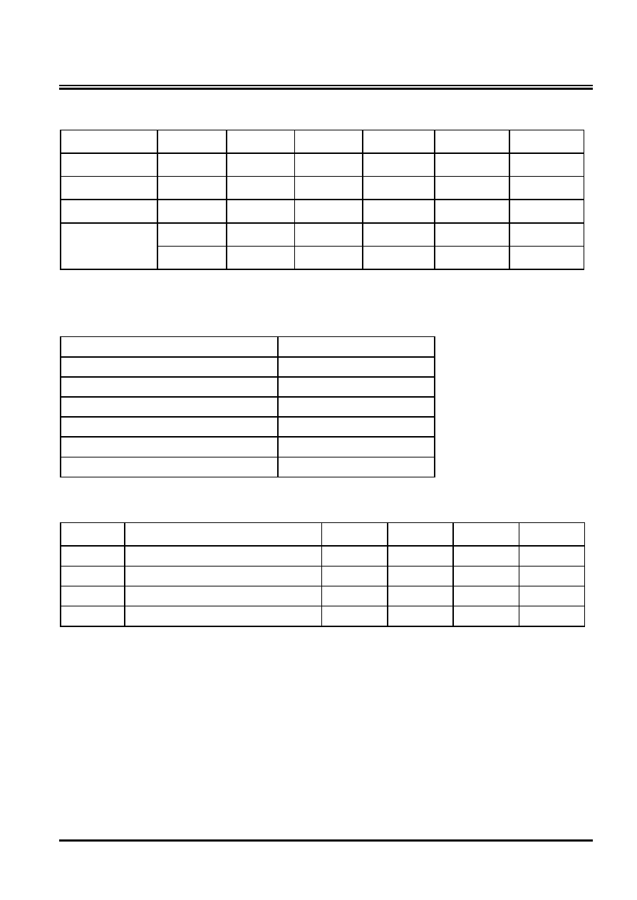
Operating Mode
Mode
CE1#
CE2
OE#
WE#
DQ0~DQ7
Power
Read
L
H
L
H
DOUT
Active
Write
L
H
X
L
DIN
Active
Output Deselect
L
H
H
H
High-Z
Active
H
X
X
X
High-Z
Standby
Standby
X
L
X
X
High-Z
Standby
Note: X = don't care. H = logic high. L = logic low.
Absolute Maximum Ratings
Supply voltage, VDD
-0.3 to +4.6V
Input voltages, VIN
-0.3 to +4.6V
Input and output voltages, VI/O
-0.5 to VDD + 0.5V
Operating temperature, TOPR
-40 to +85
∞
C
Storage temperature, TSTRG
-55 to +150
∞
C
Soldering Temperature (10s), TSOLDER
240
∞
C
Power dissipation, PD
0.6 W
DC Recommended Operating Conditions (Ta=-40
∞
C to 85
∞
C)
Symbol
Parameter
Min
Typ
Max
Unit
VDD
Power Supply Voltage
2.7
-
3.6
V
VIH
Input High Voltage
2.2
-
VDD + 0.3
(1)
V
VIL
Input Low Voltage
-0.3
(2)
-
0.6
V
VDR
Data Retention Supply Voltage
1.5
-
3.6
V
Note:
(1) Overshoot : VDD +2.0V in case of pulse width
20ns
(2) Undershoot : -2.0V in case of pulse width
20ns
EtronTech
EM562081
Preliminary
4
Rev 1.0
July 2001
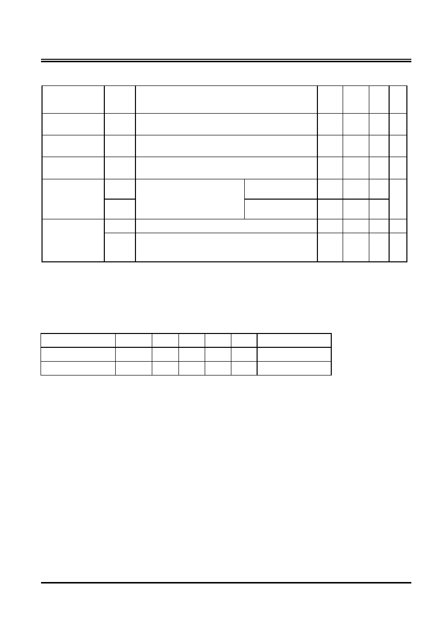
DC Characteristics
(Ta = -40
∞
C to 85
∞
C, VDD = 2.7V to 3.6V)
Parameter
Symbol
Test Conditions
Min
Typ* Max Unit
Input low current
IIL
IIN = 0V to VDD
- 1
-
1
µ
A
Output low voltage VOL
IOL = 2.1 mA
-
-
0.4 V
Output high
voltage
VOH
IOH = -1.0 mA
2.2
-
-
V
IDD1
Cycle time = min
-
10
25
Operating current
IDD2
VDD = 3.6 V , CE1# = VIL and
CE2 = VIH and IOUT = 0mA
Other Input = VIH / VIL
Cycle time = 1
µ
s
-
-
5
mA
IDDS1 CE1# = VIH or CE2 = VIL
-
-
0.5 mA
Standby current
IDDS2
**
(Note)
CE1#
VDD ≠ 0.2V or CE2
0.2V,
-
1
10
µ
A
Notes:
* Typical value are measured at T
a
= 25
∞
C, and not 100% tested.
** In standby mode with CE1#
VDD - 0.2V, these limits are assured for the condition
CE2
V
DD
- 0.2V or CE2
0.2V.
Capacitance (Ta = 25
∞
C; f = 1 MHz)
Parameter
Symbol
Min
Typ
Max
Unit
Test Conditions
Input capacitance
CIN
-
-
10
pF
VIN = GND
Output capacitance
COUT
-
-
10
pF
VOUT = GND
Notes: This parameter is periodically sampled and is not 100% tested.
EtronTech
EM562081
Preliminary
5
Rev 1.0
July 2001
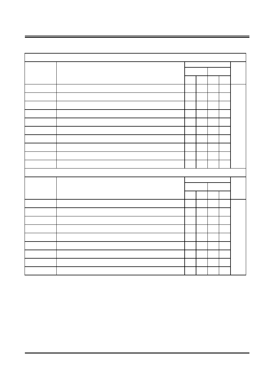
AC Characteristics and Operating Conditions (Ta = -40
∞
C to 85
∞
C, VDD = 2.7V to 3.6V)
Read Cycle
EM562081
-85
-70
Symbol
Parameter
Min Max Min Max
Unit
tRC
Read cycle time
85
-
70
-
tAA
Address access time
-
85
-
70
tCO1
Chip Enable (CE1#) Access Time
-
85
-
70
tCO2
Chip Enable (CE2) Access Time
-
85
-
70
tOE
Output enable access time
-
45
-
35
tLZ
Chip Enable Low to Output in Low-Z
10
-
10
-
tOLZ
Output enable Low to Output in Low-Z
3
-
3
-
tHZ
Chip Enable High to Output in High-Z
-
35
-
25
tOHZ
Output Enable High to Output in High-Z
-
35
-
25
tOH
Output Data Hold Time
10
-
10
-
ns
Write Cycle
EM562081
-85
-70
Symbol
Parameter
Min Max Min Max
Unit
tWC
Write cycle time
85
-
70
-
tWP
Write pulse width
55
-
55
-
tCW
Chip Enable to end of write
70
-
60
-
tAS
Address setup time
0
-
0
-
tWR
Write Recovery time
0
-
0
-
tWHZ
WE# Low to Output in High-Z
-
35
-
30
tOW
WE# High to Output in Low-Z
5
-
5
-
tDS
Data Setup Time
35
-
30
-
tDH
Data Hold Time
0
-
0
-
ns
AC Test Condition
∑
Output load: 50pF + one TTL gate
∑
Input pulse level: 0.4V, 2.4V
∑
Timing measurements: 0.5 x V
DD
∑
tR, tF: 5ns