 | –≠–ª–µ–∫—Ç—Ä–æ–Ω–Ω—ã–π –∫–æ–º–ø–æ–Ω–µ–Ω—Ç: EM637327 | –°–∫–∞—á–∞—Ç—å:  PDF PDF  ZIP ZIP |
EtronTech
EM637327
Etron Technology, Inc.
No. 6, Technology Rd. V, Science-Based Industrial Park, Hsinchu, Taiwan 30077, R.O.C
TEL: (886)-3-5782345 FAX: (886)-3-5778671
Etron Technology, Inc., reserves the right to make changes to its products and specifications without notice.
1Mega x 32 SGRAM
Preliminary (08/99)
Features
∑
Fast access time from clock: 4.5/5.5/5.5/6 ns
∑
Fast clock rate: 200/166/143/125 MHz
∑
Fully synchronous operation
∑
Internal pipelined architecture
∑
Dual internal banks (512K x 32bit x 2bank)
∑
Programmable Mode
- CAS# Latency: 1, 2, or 3
- Burst Length: 1, 2, 4, 8, or full page
- Burst Type: interleaved or linear burst
- Burst-Read-Single-Write
- Load Color or Mask register
∑
Burst stop function
∑
Individual byte controlled by DQM0-3
∑
Block write and write-per-bit capability
∑
Auto Refresh and Self Refresh
∑
2048 refresh cycles/32ms
∑
Single +3.3V
±
0.3V power supply
∑
Interface: LVTTL
∑
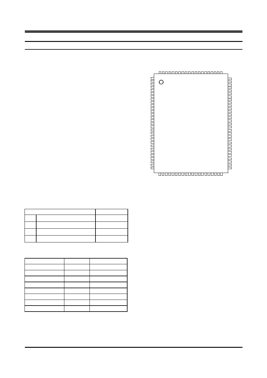
JEDEC 100-pin Plastic package
- QFP (body thickness=2.8mm)
- TQFP1.4 (body thickness=1.4mm)
Key Specifications
EM637327
- 5/6/7/8
t
CK3
Clock Cycle time(min.)
5/6/7/8 ns
t
RAS
Row Active time(max.)
25/30/35/40 ns
t
AC3
Access time from CLK(max.)
4.5/5.5/5.5/6 ns
t
RC
Row Cycle time(min.)
55/60/63/72 ns
Ordering Information
Part Number
Frequency
Package
EM637327Q-5
200 MHz
QFP
EM637327TQ-5
200 MHz
TQFP1.4
EM637327Q-6
166 MHz
QFP
EM637327TQ-6
166 MHz
TQFP1.4
EM637327Q-7
143 MHz
QFP
EM637327TQ-7
143 MHz
TQFP1.4
EM637327Q-8
125 MHz
QFP
EM637327TQ-8
125 MHz
TQFP1.4
Pin Assignment (Top View)
DQ 3
V
DDQ
DQ 4
DQ 5
V
SSQ
DQ 6
DQ 7
V
DDQ
D Q16
D Q17
V
SSQ
D Q18
D Q19
V
DDQ
V
D D
V
SS
D Q20
D Q21
V
SSQ
D Q22
D Q23
V
DDQ
DQ M0
DQ M2
WE#
CA S#
RA S#
CS 0#
B S
A 9
DQ28
V
DDQ
DQ27
DQ26
V
SSQ
DQ25
DQ24
V
DDQ
DQ15
DQ14
V
SSQ
DQ13
DQ12
V
DDQ
V
SS
V
D D
DQ11
DQ10
V
SSQ
DQ 9
DQ 8
V
DDQ
NC
DQ M3
DQ M1
CL K
CKE
DSF
NC
A8 (AP)
D
Q
2
9
V
SSQ
D
Q
3
0
D
Q
3
1
V
SS
N
C
N
C
N
C
N
C
N
C
N
C
N
C
N
C
N
C
N
C
V
D
D
DQ
0
DQ
1
V
SSQ
DQ
2
A
7
A
6
A
5
A
4
V
SS
A
1
0
N
C
N
C
N
C
N
C
N
C
N
C
N
C
N
C
N
C
V
D
D
A
3
A
2
A
1
A
0
8
1
8
2
8
3
8
4
8
5
8
6
8
7
8
8
8
9
9
0
9
1
9
2
9
3
9
4
9
5
9
6
9
7
9
8
9
9
1
0
0
1
2
3
4
5
6
7
8
9
1 0
11
1 2
1 3
1 4
1 5
1 6
1 7
1 8
1 9
2 0
2 1
2 2
2 3
2 4
2 5
2 6
2 7
2 8
2 9
3 0
8 0
7 9
7 8
7 7
7 6
7 5
7 4
7 3
7 2
7 1
7 0
6 9
6 8
6 7
6 6
6 5
6 4
6 3
6 2
6 1
6 0
5 9
5 8
5 7
5 6
5 5
5 4
5 3
5 2
5 1
5
0
4
9
4
8
4
7
4
6
4
5
4
4
4
3
4
2
4
1
4
0
3
9
3
8
3
7
3
6
3
5
3
4
3
3
3
2
3
1
Overview
The EM637327 SGRAM is a high-speed CMOS
synchronous graphics DRAM containing 32 Mbits. It is
internally configured as a dual 512K x 32 DRAM with a
synchronous interface (all signals are registered on the
positive edge of the clock signal, CLK). Each of the
512K x 32 bit banks is organized as 2048 rows by 256
columns by 32 bits. Read and write accesses to the
SGRAM are burst oriented; accesses start at a selected
location and continue for a programmed number of
locations in a programmed sequence. Accesses begin
with the registration of a BankActivate command which
is then followed by a Read or Write command.
The EM637327 provides for programmable Read
or Write burst lengths of 1, 2, 4, 8, or full page, with a
burst termination option. An auto precharge function
may be enabled to provide a self-timed row precharge
that is initiated at the end of the burst sequence. The
refresh functions, either Auto or Self Refresh are easy
to use.
By having a programmable mode register, the
system can choose the most suitable modes to
maximize its performance. These devices are well
suited for applications requiring high memory
bandwidth.
EtronTech
1Mega x 32 SGRAM
EM637327
Preliminary
2
August 1999
Block Diagram
REFRESH
COUNTER
COLUMN
COUNTER
ADDRESS
BUFFER
A0
A7
A9
A10
BS
CONTROL
SIGNAL
GENERATOR
DQ
S
BUFFER
DQM0~3
COLOR
REGISTER
MASK
REGISTER
CLOCK
BUFFER
COMMAND
DECODER
Column Decoder
Sense Amplifier
Row
Decoder
2048 X 256 X 32
CELL ARRAY
(BANK #0)
Sense Amplifier
Column Decoder
Row
Decoder
2048 X 256 X 32
CELL ARRAY
(BANK #1)
MODE
REGISTER
CLK
CKE
CS#
RAS#
CAS#
WE#
A8
DQ0
¢x
DQ31
DSF
SPECIAL
MODE
REGISTER
EtronTech
1Mega x 32 SGRAM
EM637327
Preliminary
3
August 1999
Pin Descriptions
Table 1. Pin Details of EM637327
Symbol Type Description
CLK
Input Clock: CLK is driven by the system clock. All SGRAM input signals are sampled on the
positive edge of CLK. CLK also increments the internal burst counter and controls the
output registers.
CKE
Input Clock Enable: CKE activates(HIGH) and deactivates(LOW) the CLK signal. If CKE goes
low synchronously with clock(set-up and hold time same as other inputs), the internal clock
is suspended from the next clock cycle and the state of output and burst address is frozen
as long as the CKE remains low. When both banks are in the idle state, deactivating the
clock controls the entry to the Power Down and Self Refresh modes. CKE is synchronous
except after the device enters Power Down and Self Refresh modes, where CKE becomes
asynchronous until exiting the same mode. The input buffers, including CLK, are disabled
during Power Down and Self Refresh modes, providing low standby power.
BS
Input Bank Select: BS defines to which bank the BankActivate, Read, Write, or BankPrecharge
command is being applied. BS is also used to program the 11th bit of the Mode and
Special Mode registers.
A0-A10 Input Address Inputs: A0-A10 are sampled during the BankActivate command (row address
A0-A10) and Read/Write command (column address A0-A7 with A8 defining Auto
Precharge) to select one location out of the 512K available in the respective bank. During
a Precharge command, A8 is sampled to determine if both banks are to be precharged (A8
= HIGH). The address inputs also provide the op-code during a Mode Register Set or
Special Mode Register Set command.
CS#
Input Chip Select: CS# enables (sampled LOW) and disables (sampled HIGH) the command
decoder. All commands are masked when CS# is sampled HIGH. CS# provides for
external bank selection on systems with multiple banks. It is considered part of the
command code.
RAS#
Input Row Address Strobe: The RAS# signal defines the operation commands in conjunction
with the CAS# and WE# signals and is latched at the positive edges of CLK. When RAS#
and CS# are asserted "LOW" and CAS# is asserted "HIGH," either the BankActivate
command or the Precharge command is selected by the WE# signal. When the WE# is
asserted "HIGH," the BankActivate command is selected and the bank designated by BS is
turned on to the active state. When the WE# is asserted "LOW," the Precharge command
is selected and the bank designated by BS is switched to the idle state after the precharge
operation.
CAS#
Input Column Address Strobe: The CAS# signal defines the operation commands in
conjunction with the RAS# and WE# signals and is latched at the positive edges of CLK.
When RAS# is held "HIGH" and CS# is asserted "LOW," the column access is started by
asserting CAS# "LOW." Then, the Read or Write command is selected by asserting WE#
"LOW" or "HIGH."
WE#
Input Write Enable: The WE# signal defines the operation commands in conjunction with the
RAS# and CAS# signals and is latched at the positive edges of CLK. The WE# input is
used to select the BankActivate or Precharge command and Read or Write command.
DSF
Input Define Special Function: The DSF signal defines the operation commands in conjunction
with the RAS# and CAS# and WE# signals and is latched at the positive edges of CLK.
The DSF input is used to select the masked write disable/enable command and block write
command, and the Special Mode Register Set cycle.
EtronTech
1Mega x 32 SGRAM
EM637327
Preliminary
4
August 1999
DQM0 -
DQM3
Input Data Input/Output Mask: DQM0-DQM3 are byte specific, nonpersistent I/O buffer
controls. The I/O buffers are placed in a high-z state when DQM is sampled HIGH. Input
data is masked when DQM is sampled HIGH during a write cycle. Output data is masked
(two-clock latency) when DQM is sampled HIGH during a read cycle. DQM3 masks DQ31-
DQ24, DQM2 masks DQ23-DQ16, DQM1 masks DQ15-DQ8, and DQM0 masks DQ7-
DQ0.
DQ0-
DQ31
Input/
Output
Data I/O: The DQ0-31 input and output data are synchronized with the positive edges of
CLK. The I/Os are byte-maskable during Reads and Writes. The DQs also serve as
column/byte mask inputs during Block Writes.
NC
-
No Connect: These pins should be left unconnected.
V
DDQ
Supply DQ Power: Provide isolated power to DQs for improved noise immunity.
V
SSQ
Supply DQ Ground: Provide isolated ground to DQs for improved noise immunity.
V
DD
Supply Power Supply: +3.3V
±
0.3V
V
SS
Supply Ground
EtronTech
1Mega x 32 SGRAM
EM637327
Preliminary
5
August 1999
Operation Mode
Fully synchronous operations are performed to latch the commands at the positive edges of CLK.
Table 2 shows the truth table for the operation commands.
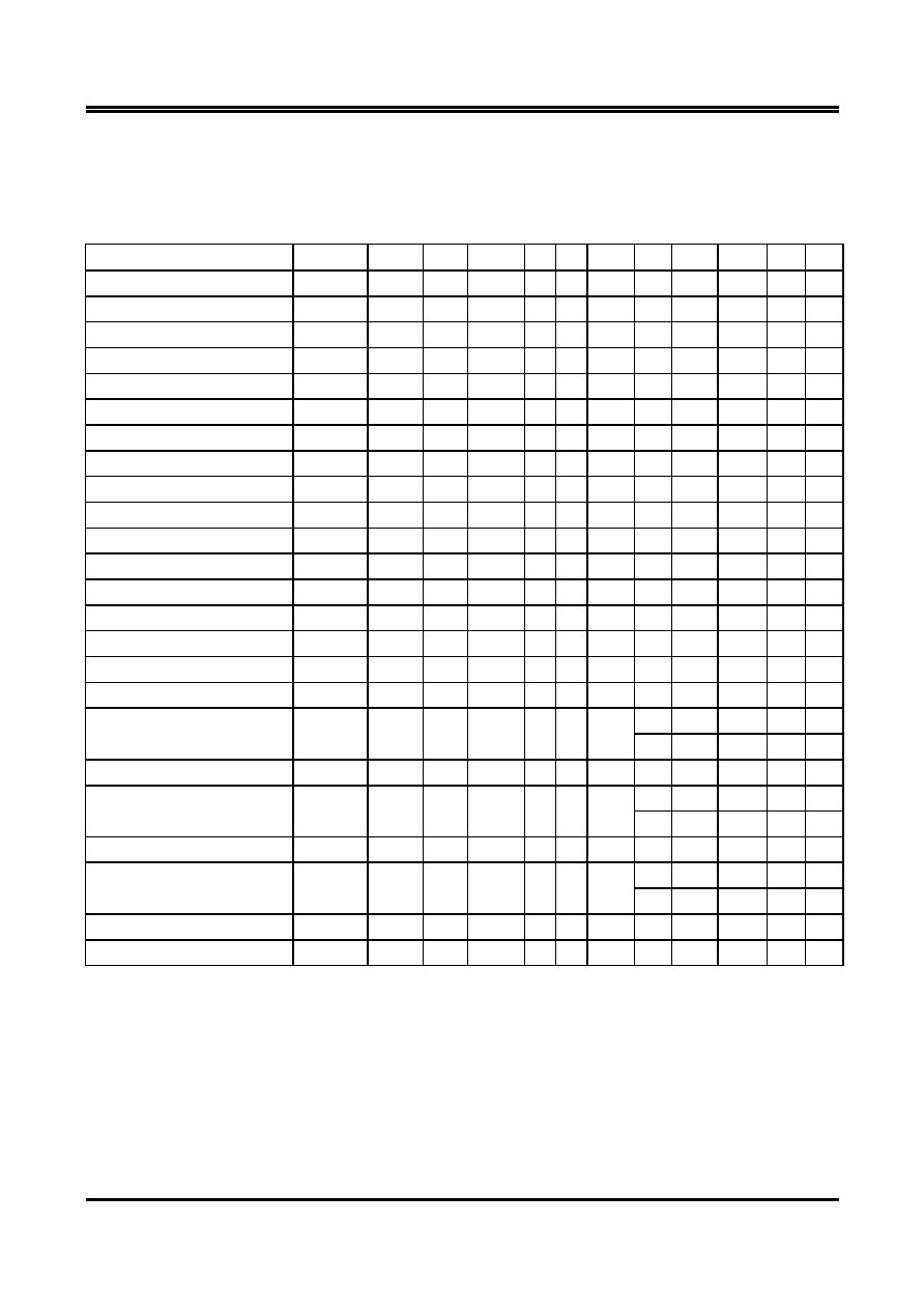
Table 2. Truth Table (Note (1), (2) )
Command
State
CKE
n-1
CKE
n
DQM
(7)
BS A8 A
DDR
CS# RAS# CAS# WE# DSF
BankActivate & Masked Write Disable
Idle
(3)
H
X
X
V
V
V
L
L
H
H
L
BankActivate & Masked Write Enable
Idle
(3)
H
X
X
V
V
V
L
L
H
H
H
BankPrecharge
Any
H
X
X
V
L
X
L
L
H
L
L
PrechargeAll
Any
H
X
X
X
H
X
L
L
H
L
L
Write
Active
(3)
H
X
X
V
L
V
L
H
L
L
L
Block Write Command
Active
(3)
H
X
X
V
L
V
L
H
L
L
H
Write and AutoPrecharge
Active
(3)
H
X
X
V
H
V
L
H
L
L
L
Block Write and AutoPrecharge
Active
(3)
H
X
X
V
H
V
L
H
L
L
H
Read
Active
(3)
H
X
X
V
L
V
L
H
L
H
L
Read and Autoprecharge
Active
(3)
H
X
X
V
H
V
L
H
L
H
L
Mode Register Set
Idle
H
X
X
V
L
V
L
L
L
L
L
Special Mode Register Set
Idle
(5)
H
X
X
X
X
V
L
L
L
L
H
No-Operation
Any
H
X
X
X
X
X
L
H
H
H
X
Burst Stop
Active
(4)
H
X
X
X
X
X
L
H
H
L
L
Device Deselect
Any
H
X
X
X
X
X
H
X
X
X
X
AutoRefresh
Idle
H
H
X
X
X
X
L
L
L
H
L
SelfRefresh Entry
Idle
H
L
X
X
X
X
L
L
L
H
L
SelfRefresh Exit
Idle
L
H
X
X
X
X
H
X
X
X
X
(SelfRefresh)
L
H
H
H
X
Clock Suspend Mode Entry
Active
H
L
X
X
X
X
X
X
X
X
X
Power Down Mode Entry
Any
(6)
H
L
X
X
X
X
H
X
X
X
X
L
H
H
H
L
Clock Suspend Mode Exit
Active
L
H
X
X
X
X
X
X
X
X
X
Power Down Mode Exit
Any
L
H
X
X
X
X
H
X
X
X
X
(PowerDown)
L
H
H
H
L
Data Write/Output Enable
Active
H
X
L
X
X
X
X
X
X
X
X
Data Mask/Output Disable
Active
H
X
H
X
X
X
X
X
X
X
X
Note:
1. V=Valid X=Don't Care L=Low level H=High level
2. CKE
n
signal is input level when commands are provided.
CKE
n-1
signal is input level one clock cycle before the commands are provided.
3. These are states of bank designated by BS signal.
4. Device state is 1, 2, 4, 8, and full page burst operation.
5. The Special Mode Register Set is also available in Row Active State.
6. Power Down Mode can not enter in the burst operation.
When this command is asserted in the burst cycle, device state is clock suspend mode.
7. DQM0-3