EtronTech
EM6A9325
Etron Technology, Inc.
No. 6, Technology Rd. V, Science-Based Industrial Park, Hsinchu, Taiwan 30077, R.O.C
TEL: (886)-3-5782345
FAX: (886)-3-5778671
Etron Technology, Inc., reserves the right to make changes to its products and specifications without notice.
4M x 32 Low Power SDRAM
Advance 07/2002
Features
∑
Fast clock rate : 133/100 MHz
∑
Fully synchronous operation
∑
Internal pipelined architecture
∑
Four internal banks ( 1M x 32bit x 4bank )
∑
Programmable Mode
-CAS# Latency : 1, 2 & 3
-Burst Length : 1,2,4,8, & full page
-Burst Type : Sequential & Interleave
∑
Burst-Read-Single-Write
∑
Burst stop function
∑
Individual byte controlled by DQM0-3
∑
Auto Refresh and Self Refresh
∑
4096 refresh cycles / 64ms
∑
2.5V power supply
∑
Interface : LVTTL
∑
Package : 90 ball-FBGA, 11x13mm
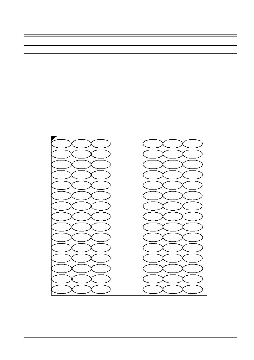
Pin Assignment : Top View
0
/
.
-
+
*
)
(
'
&
%
$
'4
'4
'4
9
"
9VV
"
'4
9VV
"
'4
9
'4
9
"
9
$$"
'4
'4
'4
9
"
9
"
'4
9VV
'40
$
$
$
$
'4
9
$$"
1&
'4
'40
9
$
$
&/.
&.(
'40
1&
9
"
'4
9
$$"
'4
$
$
1&
$
&$6
%$
'40
:(
9
$$"
'4
9
$$"
'4
9
"
9
"
'4
'4
'4
9
"
'4
DQ15
1
3
5
'4
'4
9
"
%$
&6
5$6
'4
'4
9
"
9
9
$$"
'4
9
'4
'4
9
$$
9
$$"
'4
'4
1&
$
$
1&
$
1&
9
$$
'4
'4
9
$$"
9
$$
EtronTech
EM6A9325
Advance
2 July
2002
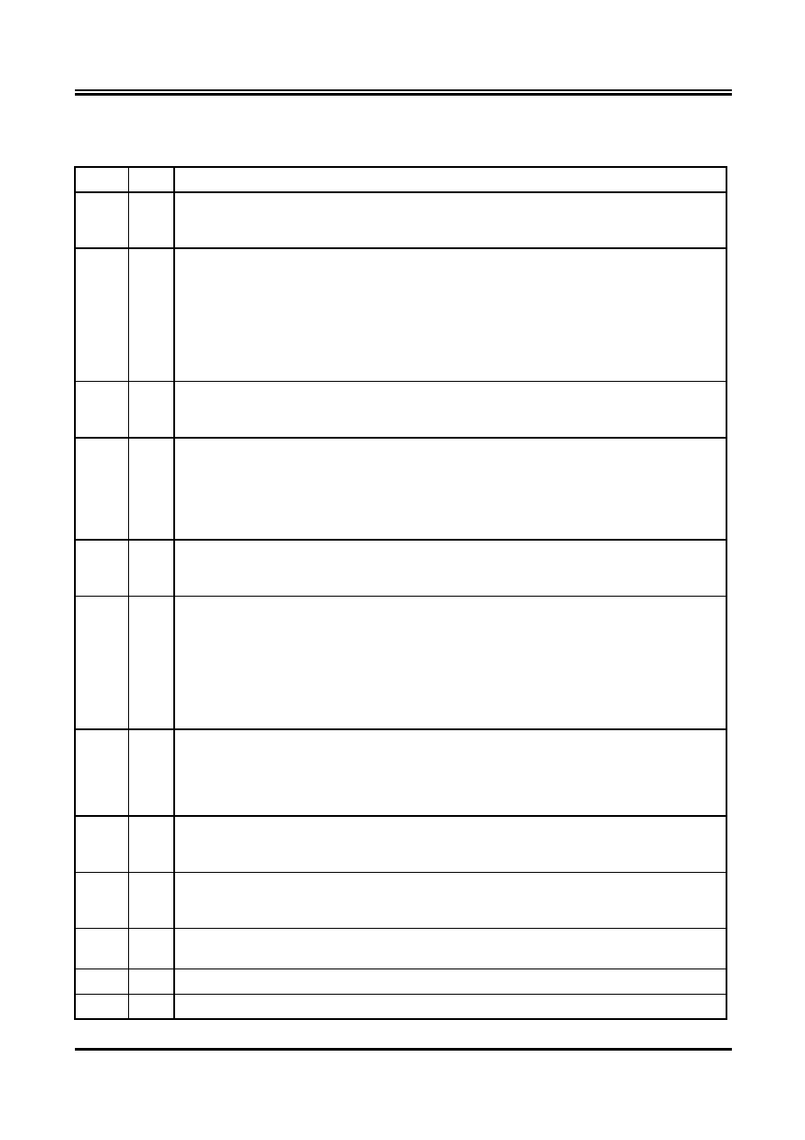
Pin Descriptions
Table 1. Pin Details of 4Mx32 LPSDRAM
Symbol Type Description
CLK Input
Clock: CLK is driven by the system clock. All SDRAM input signals are sampled on the
positive edge of CLK. CLK also increments the internal burst counter and controls the
output registers.
CKE Input
Clock Enable: CKE activates(HIGH) and deactivates(LOW) the CLK signal. If CKE goes
low synchronously with clock(set-up and hold time same as other inputs), the internal clock
is suspended from the next clock cycle and the state of output and burst address is frozen
as long as the CKE remains low. When all banks are in the idle state, deactivating the clock
controls the entry to the Power Down and Self Refresh modes. CKE is synchronous except
after the device enters Power Down and Self Refresh modes, where CKE becomes
asynchronous until exiting the same mode. The input buffers, including CLK, are disabled
during Power Down and Self Refresh modes, providing low standby power.
BA0,
BA1
Input Bank Select: BA0 and BA1 defines to which bank the BankActivate, Read, Write, or
BankPrecharge command is being applied. BS is also used to program the 11th bit of the
Mode and Special Mode registers.
A0-A11 Input Address Inputs: A0-A10 are sampled during the BankActivate command (row address A0-
A10) and Read/Write command (column address A0-A7 with A10 defining Auto Precharge)
to select one location out of the 256K available in the respective bank. During a Precharge
command, A10 is sampled to determine if all banks are to be precharged (A10 = HIGH).
The address inputs also provide the op-code during a Mode Register Set or Special Mode
Register Set command.
CS# Input
Chip Select: CS# enables (sampled LOW) and disables (sampled HIGH) the command
decoder. All commands are masked when CS# is sampled HIGH. CS# provides for external
bank selection on systems with multiple banks. It is considered part of the command code.
RAS# Input
Row Address Strobe: The RAS# signal defines the operation commands in conjunction
with the CAS# and WE# signals and is latched at the positive edges of CLK. When RAS#
and CS# are asserted "LOW" and CAS# is asserted "HIGH," either the BankActivate
command or the Precharge command is selected by the WE# signal. When the WE# is
asserted "HIGH," the BankActivate command is selected and the bank designated by BS is
turned on to the active state. When the WE# is asserted "LOW," the Precharge command is
selected and the bank designated by BS is switched to the idle state after the precharge
operation.
CAS#
Input Column Address Strobe: The CAS# signal defines the operation commands in
conjunction with the RAS# and WE# signals and is latched at the positive edges of CLK.
When RAS# is held "HIGH" and CS# is asserted "LOW," the column access is started by
asserting CAS# "LOW." Then, the Read or Write command is selected by asserting WE#
"LOW" or "HIGH."
WE# Input
Write Enable: The WE# signal defines the operation commands in conjunction with the
RAS# and CAS# signals and is latched at the positive edges of CLK. The WE# input is used
to select the BankActivate or Precharge command and Read or Write command.
DQM0 -
DQM3
Input Data Input/Output Mask: Data Input Mask: DM0-DM3 are byte specific. Input data is
masked when DM is sampled HIGH during a write cycle. DM3 masks DQ31-DQ24, DM2
masks DQ23-DQ16, DM1 masks DQ15-DQ8, and DM0 masks DQ7-DQ0.
DQ0-
DQ31
Input/
Output
Data I/O: The DQ0-31 input and output data are synchronized with the positive edges of
CLK. The I/Os are byte-maskable during Reads and Writes.
NC -
No Connect: These pins should be left unconnected.
V
DDQ
Supply DQ Power: Provide isolated power to DQs for improved noise immunity.

EtronTech
EM6A9325
Advance
3 July
2002
V
SSQ
Supply DQ Ground: Provide isolated ground to DQs for improved noise immunity.
V
DD
Supply Power Supply: +2.5V
±
0.2V
V
SS
Supply Ground
EtronTech
EM6A9325
Advance
4 July
2002
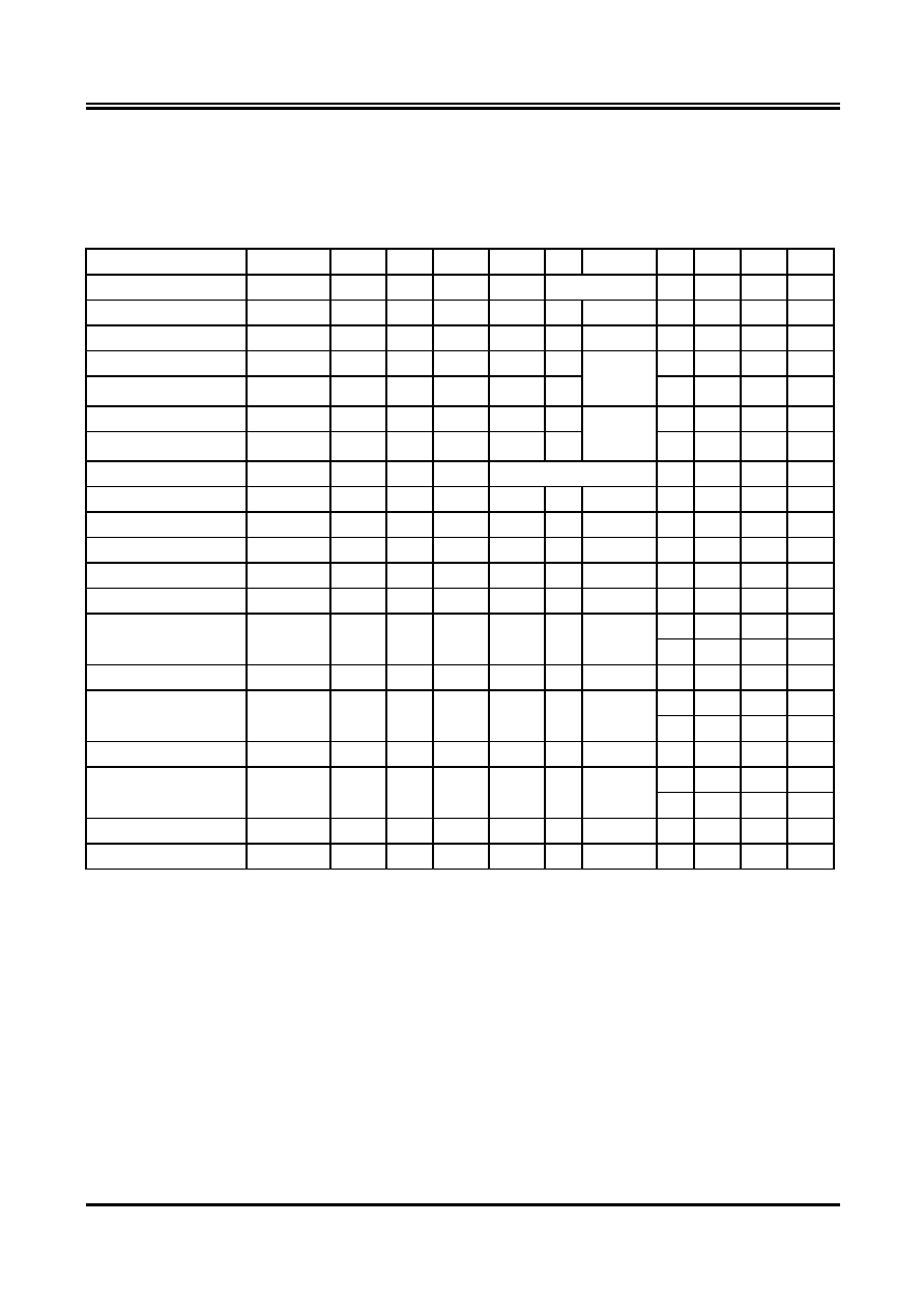
Operation Mode
Fully synchronous operations are performed to latch the commands at the positive edges of CLK.
Table 2 shows the truth table for the operation commands.
Table 2. Truth Table ( Note (1) , (2) )
Command State
CKE
n-1
CKE
n
DQM
(6)
BA
0,1
A
10
A
11
, A
9-0
CS# RAS# CAS# WE#
Bank Activate
Idle
(3)
H X X V Row
address
L L H H
Bank Precharge
Any H X X V
L X L
L
H
L
Precharge All
Any
H X X X H X L L H L
Write
Active
(3)
H X X V L
L
H L L
Write and Auto Precharge
Active
(3)
H X X V H
Column
address
(A0 ~ A7)
L H L L
Read
Active
(3)
H X X V L
L H L H
Read and Auto precharge
Active
(3)
H X X V H
Column
address
(A0 ~ A7)
L H L H
Mode Register Set
Idle H X X
OP
code
L L L L
No-Operation
Any H X X X
X X L
H
H
H
Burst Stop
Active
(4)
H X X X
X X L
H
H
L
Device Deselect
Any
H X X X X X H X X X
Auto Refresh
Idle H H X X
X X L
L
L
H
Self Refresh Entry
Idle H L X X
X X L
L
L
H
Self Refresh Exit
Idle
L H X X X X H X X X
(Self Refresh)
L H H H
Clock Suspend Mode Entry
Active H L X X
X X X
X
X
X
Power Down Mode Entry
Any
(5)
H L X X X X H X X X
L H H H
Clock Suspend Mode Exit
Active L H X X
X X X
X
X
X
Power Down Mode Exit
Any
L H X X X X H X X X
(Power Down)
L H H H
Data Write/Output Enable
Active H X L X X X X X X X
Data Mask/Output Disable
Active H X H X X X X X X X
Note: 1. V = Valid, X = Don't care, L = Logic low, H = Logic high
2. CKE
n
signal is input level when commands are provided.
CKE
n-1
signal is input level one clock cycle before the commands are provided.
3. These are states of bank designated by BA signal.
4. Device state is 1, 2, 4, 8, and full page burst operation.
5. Power Down Mode can not enter in the burst operation.
When this command is asserted in the burst cycle, device state is clock suspend mode.
6. DQM0-3
EtronTech
EM6A9325
Advance
5 July
2002
Mode Register Set (MRS)
The mode register is divided into various fields depending on functionality.
∑
Burst Length Field (A2, A1, A0) :This field specifies the data length of column access and selects the
Burst Length.
∑
Addressing Mode Select Field (A3) : The Addressing Mode can be Interleave Mode or Sequential
Mode. Both Sequential Mode and Interleave Mode support burst length of 1, 2, 4 and 8. Full page
burst length is only for Sequential mode.
∑
CAS# Latency Field (A6, A5, A4) : This field specifies the number of clock cycles from the assertion
of the Read command to the first read data. The minimum whole value of CAS# Latency depends on
the frequency of CK. The minimum whole value satisfying the following formula must be programmed
into this field. t
CAC
(min)
CAS# Latency X t
CK
∑
Test Mode Field (A7, A8) : These two bits must be programmed to "00" in normal operation.
∑
W.B.L : Write Burst Length Field (A9) : This bit is used to select the burst write length.
Mode Resistor Bitmap
BA1
BA0
A11
A10 A9 A8 A7 A6 A5 A4 A3 A2 A1 A0
RFU
RFU
W.B.L
TM
CAS Latency
BT
Burst Length
A9 Length A8
A7 Mode
A3 Type
0 Burst 0 0 Normal 0
Sequential
1 Single
Bit 1 0
Reserved 1
Interleave
0
1
Reserved
A6
A5
A4
CAS Latency
A2
A1
A0
Burst Length
0 0 0
Reserved
0 0 0
1
0 0 1
1
clock
0 0 1
2
0 1 0
2
clocks
0 1 0
4
0 1 1
3
clocks
0 1 1
8
1 0 1
Reserved
1 1 1
Full
Page
(Sequential)
All other Reserved
All other Reserved
Burst Definition, Addressing Sequence of Sequential and Interleave Mode
Start Address
Burst Length
A2 A1 A0
Sequential Interleave
X
X
0
0, 1
0, 1
2
X
X
1
1, 0
1, 0
X
0
0
0, 1, 2, 3
0, 1, 2, 3
X
0
1
1, 2, 3, 0
1, 0, 3, 2
X
1
0
2, 3, 0, 1
2, 3, 0, 1
4
X
1
1
3, 0, 1, 2
3, 2, 1, 0
0
0
0
0, 1, 2, 3, 4, 5, 6, 7
0, 1, 2, 3, 4, 5, 6, 7
0
0
1
1, 2, 3, 4, 5, 6, 7, 0
1, 0, 3, 2, 5, 4, 7, 6
0
1
0
2, 3, 4, 5, 6, 7, 0, 1
2, 3, 0, 1, 6, 7, 4, 5
0
1
1
3, 4, 5, 6, 7, 0, 1, 2
3, 2, 1, 0, 7, 6, 5, 4
1
0
0
4, 5, 6, 7, 0, 1, 2, 3
4, 5, 6, 7, 0, 1, 2, 3
1
0
1
5, 6, 7, 0, 1, 2, 3, 4
5, 4, 7, 6, 1, 0, 3, 2
1
1
0
6, 7, 0, 1, 2, 3, 4, 5
6, 7, 4, 5, 2, 3, 0, 1
8
1
1
1
7, 0, 1, 2, 3, 4, 5, 6
7, 6, 5, 4, 3, 2, 1, 0