Pr
eli
mi
na
ry
FEATURES
High Voltage Operation : V
DS
=50V
High Gain: 15dB(typ.) at P
out
=45dBm(Avg.)
High Efficiency: 32%(typ.) at P
out
=45dBm(Avg.)
Broad Frequency Range : 2100 to 2200MHz
Proven Reliability
DESCRIPTION
The EGN21A180IV is a 180 Watt GaN-HEMT that offers high efficiency,
high gain, ease of matching, greater consistency and broad bandwidth
for high power L-band amplifiers with 50V operation. This device is
targeted for high voltage, low current operation in digitally modulated
base station applications - ideally suited for W-CDMA base station
amplifiers and other HPA designs while offering ease of use.
ABSOLUTE MAXIMUM RATINGS
Item Symbol Condition Rating Unit
Drain-Source Voltage V
DS
120 V
Gate-Source Voltage V
GS
T
c
=25
o
C -5 V
Total Power Dissipation P
t
321 W
Storage Temperature T
stg
-65 to +175
o
C
Channel Temperature T
ch
250
o
C
ELECTRICAL CHARACTERISTICS (Case Temperature Tc=25
o
C)
Item Symbol Condition Limit Unit
Min. Typ. Max.
Pinch-Off Voltage V
p
V
DS
=50V I
DS
=72mA -1.0 -2.0 -3.5 V
Gate-Drain Breakdown Voltage V
GDO
I
GS
=- 36 mA
- -350 - V
3rd Order Inter modulation Distortion IM
3
V
DS
=50V - -32 - dBc
Power Gain G
p
I
DS(DC)
=1.0A 14.0 15.0 - dB
Drain Efficiency
d
P
out
=45dBm(Avg.) - 32 - %
Note 1
Thermal Resistance R
th
Channel to Case - 0.55 0.7
o
C/W
Note 1 : IM3 and Gain test condition as follows:
IM3 & Gain : fo=2.135GHz, f1=2.145GHz W-CDMA(3GPP3.4 12-00) BS-1 64ch
67% clipping modulation(Peak/Avg. = 8.5dB@0.01% Probability(CCDF)) measured
over 3.84MHz at fo-10MHz and fI+10MHz.
Edition 1.0
June 2005
1
RECOMMENDED OPERATING CONDITION(Case Temperature Tc= 25
o
C)
Item Symbol Condition Limit Unit
DC Input Voltage V
DS
50 V
Forward Gate Current I
GF
R
G
=2
<38.8 mA
Reverse Gate Current I
GR
R
G
=2
>-14.4
mA
Channel Temperature T
ch
200
o
C
EGN21A180IV
High Voltage - High Power GaN-HEMT
Preliminary
Eudyna GaN-HEMT 180W
Pr
eli
mi
na
ry
2
EGN21A180IV
High Voltage - High Power GaN-HEMT
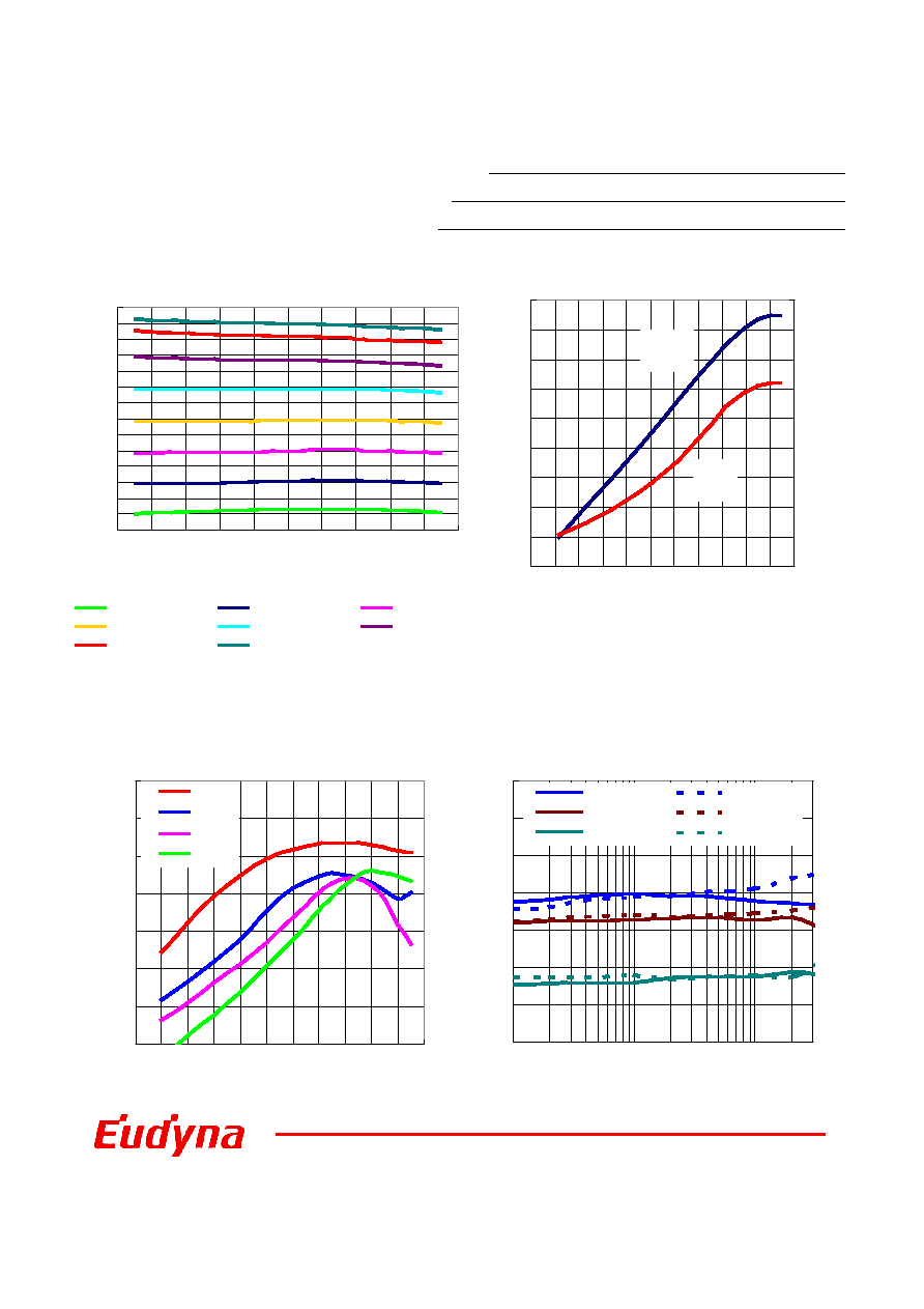
Output Power vs. Frequency
V
DS
=50V, I
DS
=1.0A
2-tone IMD vs. Output Power
V
DS
=50V, f
1
=2.135GHz, f
2
=2.145GHz, 10MHz Spacing
2-tone IMD vs. Tone Spacing, V
DS
=50V, I
DS
=1.0A
P
out
=45dBm(average) Center Frequency=2.14GHz
Output Power and Drain Efficiency vs. Input Power
V
DS
=50V, I
DS
=1.0A, f=2.14GHz
Dr
ain Efficien
cy [%]
-55
-50
-45
-40
-35
-30
-25
-20
2-tone Spacing [MHz]
IMD [dBc]
IM3 lower
IM3 upper
IM5 lower
IM5 upper
IM7 lower
IM7 upper
0.1
1.0
10
-55
-50
-45
-40
-35
-30
-25
-20
26 28 30 32 34 36 38 40 42 44 46 48
Output Power(average) [dBm]
IM3 [dBc]
0.5A
1.0A
1.5A
2.0A
40
42
44
46
48
50
52
54
2.04 2.06 2.08 2.1 2.12 2.14 2.16 2.18 2.2 2.22 2.24
Frequency [GHz]
Output Powe
r [dBm]
Pin=26dBm
Pin=28dBm
Pin=30dBm
Pin=32dBm
Pin=34dBm
Pin=36dBm
Pin=38dBm
Pin=40dBm
36
38
40
42
44
46
48
50
52
54
20 22 24 26 28 30 32 34 36 38 40 42
Input Power [dBm]
Output Powe
r [dBm]
0
10
20
30
40
50
60
70
80
90
Output
Power
Drain
Effi.

Pr
eli
mi
na
ry
3
EGN21A180IV
High Voltage - High Power GaN-HEMT
2-Carrier IMD, Drain Efficiency and Power Gain vs. Output Power
V
DS
=50V, I
DS
=1.0A, f
1
=2.135GHz, f
2
=2.145GHz(10MHz Spacing)
Peak/Avg. = 8.5dB@0.01% Probability(CCDF)
2-Carrier ACLR, Drain Efficiency and Power Gain
vs. Output Power with DPD Operation (note
V
DS
=50V, I
DS
=1.0A
f
1
=2.1375GHz, f
2
=2.1425GHz(5MHz Spacing)
Peak/Avg. = 6.5dB@0.01% Probability(CCDF);
Single Carrier Signal
Note) Digital Predistortion evaluation test system:
PMC-Sierra PALADIN-15 DPD chip-set
Dr
ain Efficien
cy [%], Pow
e
r
G
a
in
[d
B]
Output Power [dBm]
ACLR(5MHz offset) [dBc]
Dr
ain Efficien
cy [%], Pow
e
r
G
a
in
[d
B]
10
dB
/d
iv
2-carrier Spectrum with DPD Operation
DPD-OFF
DPD-ON
Center Frequency=2.14GHz
5MHz/div
Pave=45dBm
-60
-55
-50
-45
-40
-35
-30
-25
-20
-15
28
30
32
34
36
38
40
42
44
46
48
Output Power [dBm]
IMD [dBc]
0
5
10
15
20
25
30
35
40
45
Drain
Effi.
IM3
Power
Gain
IM5
IM7
-60
-55
-50
-45
-40
-35
-30
-25
-20
-15
32
34
36
38
40
42
44
46
48
0
5
10
15
20
25
30
35
40
45
Drain
Effi.
ACLR
DPD-OFF
Power
Gain
ACLR
DPD-ON
