Features
∑ Low voltage of +3.3 V or +5.0V single power
supply
∑ 10 k
high transimpedance
∑ 35 dB high gain
∑ 0 dBm large optical input
∑ Over 32 dB wide dynamic range
∑ Differential output
Applications
∑ Preamplifier of an optical receiver circuit for
OC-12/STM-4 (622 Mb/s)
Functional Description
The F0100209B is a stable GaAs integrated transimpedance amplifier capable of 35 dB
gain at a typical 200 MHz 3 dB-cutoff-frequency, making it ideally suited for a 622 Mb/s
optical receiver circuit, for example, OC-12/STM-4, instrumentation, and measurement ap-
plications. The integrated feedback loop design provides broad bandwidth and stable opera-
tion. The F0100209B typically specifies a high transimpedance of 10 k
(Rs=RL=50
) with
a wide dynamic range of over 32 dB. It also provides a large optical input overload of more
than 0dBm. Furthermore, it can operate with a low supply voltage of single +3.3 V or +5.0V.
It features a typical dissipation current of 36 mA.
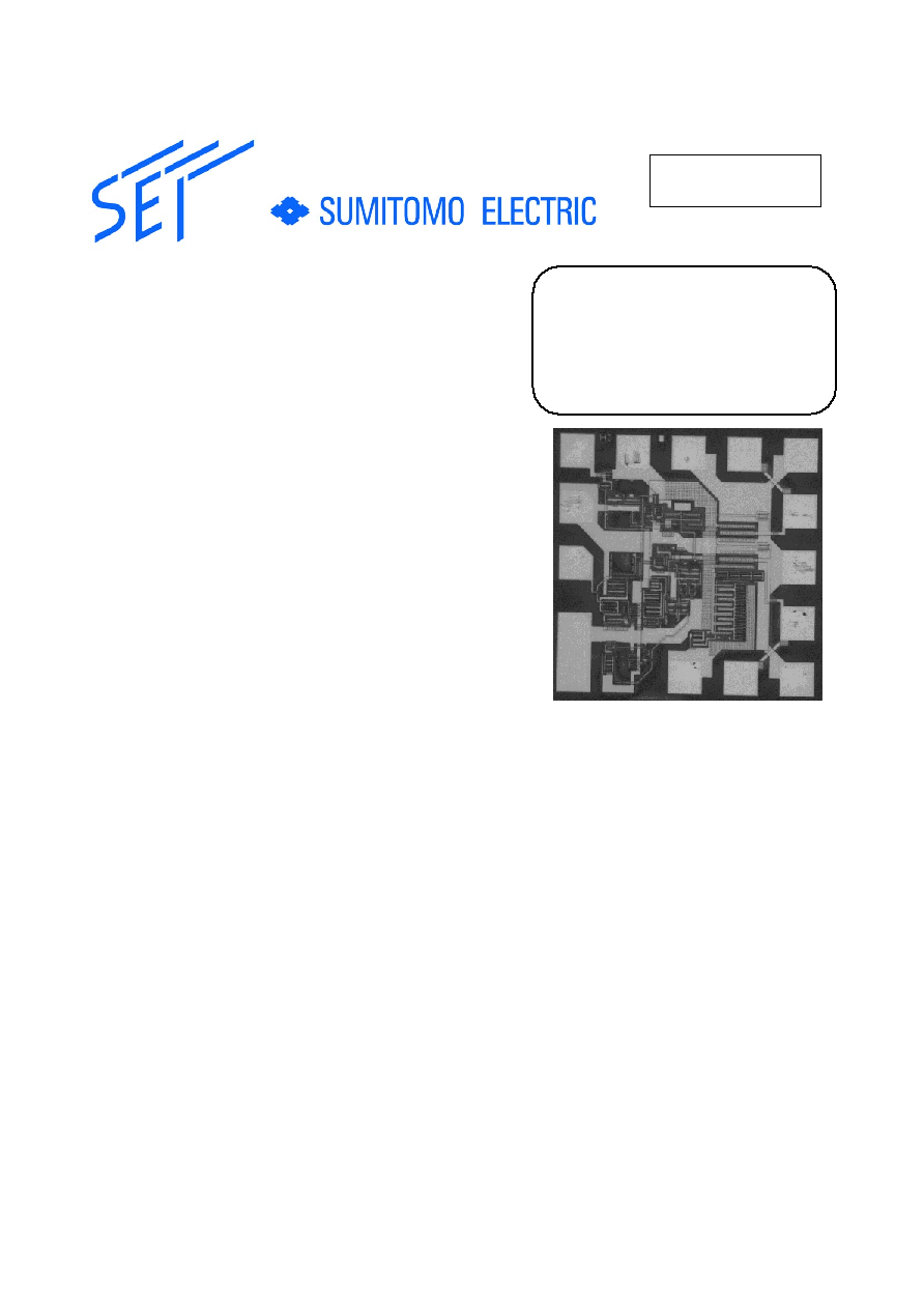
Only chip-shipment is available for all product lineups of GaAs transimpedance amplifi-
ers, because the packaged preamplifier can not operate with the maximum performance
owing to parasitic capacitance of the package.
01.08.28
ADVANCE
Transimpedance Amplifier
F0100209B
3.3 V /5V 622 Mb/s Receiver

3.3 V / 5V 622 Mb/s Transimpedance Amplifier
F0100209B
General Description
A transimpedance amplifier is applied as a pre-amplifier which is an amplifier for a faint
photo-current from a PIN photo diode (PD). The performance in terms of sensitivity, band-
width, and so on, obtained by this transimpedance amplifier strongly depend on the capaci-
tance brought at the input terminal; therefore, "typical", "minimum", or "maximum" parameter
descriptions can not always be achieved according to the employed PD and package, the
assembling design, and other technical experts. This is the major reason that there is no
product lineup of packaged transimpedance amplifiers.
Thus, for optimum performance of the transimpedance amplifier, it is essential for cus-
tomers to design the input capacitance carefully.
Hardness to electro-magnetic interference and fluctuation of a power supply voltage is
also an important point of the design, because very faint photo-current flows into the
transimpedance amplifier. Therefore, in the assembly design of the interconnection be-
tween a PD and a transimpedance, noise should be taken into consideration.
Low Voltage Operation
The F0100209B features a single 3.3 V supply operation, which is in great demand re-
cently, because most of logic IC's operate with the supply voltage of 3.3 V. The analog IC's
with a single 3.3 V supply for use in fiber optic communication systems are offered by only
SEI.
Recommendation
SEI basically recommends the F08 series PINAMP modules for customers of the
transimpedance amplifiers. In this module, a transimpedance amplifier, a PD, and a noise
filter circuit are mounted on a TO-18-can package hermetically sealed by a lens cap, having
typically a fiber pigtail. The F08 series lineups are the best choice for customers to using the
F01 series transimpedance amplifiers. SEI's F08 series allows the customers to resolve
troublesome design issues and to shorten the development lead time.
Noise Performance
The F0100209B based on GaAs FET's shows excellent low-noise characteristics com-
pared with IC's based on the silicon bipolar process. Many transmission systems often
demand superior signal-to-noise ratio, that is, high sensitivity; the F0100209B is the best


