
F0100504B 3.3V/5V 2.5Gbps Transimpedance Amplifier
02.09.02
Features
F0100504B
3.3V/5V 2.5Gb/s NRZ Receiver
Transimpedance Amplifier
-
2.2k
high transimpedance
-
29dB gain
-
Low noise (typ.6p
/
z@100MHz)
-
Typical 1900MHz O/E Bandwidth
-
Over 25dB wide dynamic range
-
3.3V or 5.0V single Voltage Supply operation
-
Differential output
Applications
-
Preamplifier of an optical receiver circuit for OC-48/STM-16 (2.5Gb/s)
Functional Description
The F0100504B is stable GaAs integrated transimpedance amplifier. Typical Applications are for 2.5Gb/s
optical receiver circuit, for example, OC-48/STM-16, instrumentation, and measurement applications. The
integrated feedback loop design provides broad bandwidth and stable operation. The F0100504B typically
specifies a high transimpedance of 2.2k
(RL=50
) at a typical 1900MHz O/E bandwidth (-3dB-cutoff
frequency) with a dynamic range of over 26dB. It also provides a large optical input overload of more than
+1dBm. Furthermore, it can operate with a low supply voltage of single +3.3V. It features a typical dissipation
current of 50mA.
Only chip-shipment is available for all product lineups of GaAs transimpedance amplifiers, because the
packaged preamplifier cannot operate with the maximum performance owing to parasitic element of the package
.

F0100504B 3.3V/5V 2.5Gbps Transimpedance Amplifier
Absolute Maximum Ratings
All published data at Ta=25
�
C unless otherwise indicated. This device isn't guaranteed opto-electric
characteristics in these ranges. At least, this device isn't broken in these ranges.
VSS=0V
Parameter Symbol
Value
Units Attentions
Supply Voltage
VDD3.3
-0.3 to +5.0V
V
at 3.3V operation
Supply Voltage
VDD5.0
-0.3 to +7.0V
V
at 5.0V operation
Input Current
Iinpeak
4
mA
-
Ambient Operating Temperature
Ta
-40 to +90
�
C -
Storage Temperature
Tstg
-50 to 125
�
C -
Recommended Operating Conditions
VSS=0V,unless specified
Value
Parameter Symbol
MIN.
TYP.
MAX.
Unit Attentions
Supply Voltage
VDD3.3
3.10
3.30
3.60
V
at 3.3V operation
Supply Voltage
VDD5.0
4.75
5.00
5.25
V
at 5.0V operation
Operating Temperature
Tc*
0
25
85
�
C
Input Capacitance
Cpd
-
0.3
-
pF
* Tc:Back side temperature of wafer
F0100504B 3.3V/5V 2.5Gbps Transimpedance Amplifier
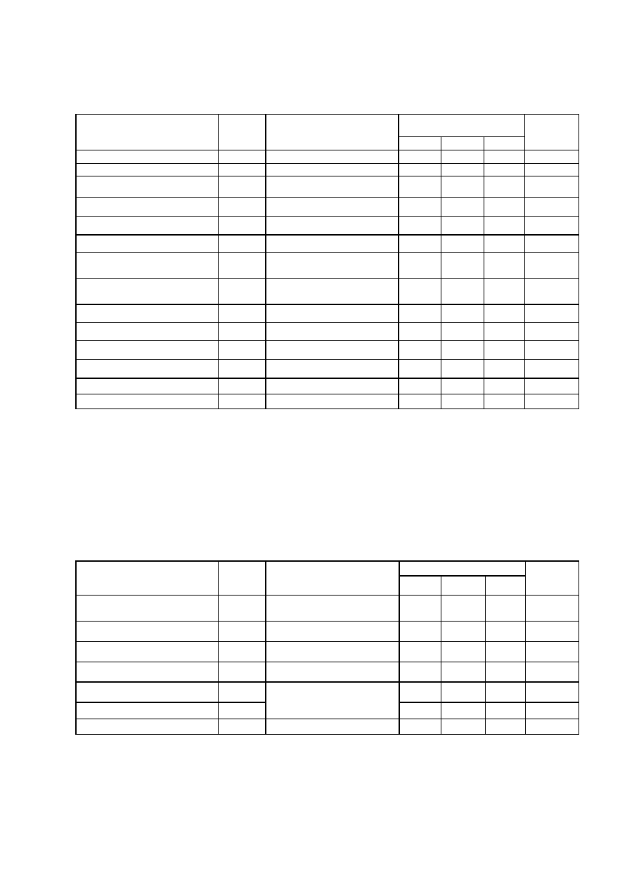
Electrical Characteristics
Tc*=0 to 85
�
C, VDD3.3=3.1 to 3.6V, VSS=0V,unless specified
Value
Parameters Symbol
Test
Conditions
MIN. TYP. MAX
Units
Supply Current
IDD
DC
35
50
65
mA
Input Voltage
Vi
*1
0.7
0.94
1.1
V
Output Voltage (positive) Vop
*1
1.6
2.1
2.6
V
Output Voltage (negative) Von *1
1.6
2.1
2.6
V
Gain (positive)
S21p
Single-ended, f=1MHz *1
27.0
29.0
33.0
dB
Gain (negative)
S21n
Single-ended, f=1MHz *1
27.0
29.0
33.0
dB
-3dB High Frequency
Cut-off (positive)
Fcp S21p-3dB
900
1200
1500
MHz
-3dB High Frequency
Cut-off (positive)
Fcn S21p-3dB
850
1050
1400
MHz
Input Impedance
Ri
f =1MHz, *1
85
100
120
Output Impedance (positive)
Rout
f =1MHz, *1
35
55
75
Output Impedance (negative)
Rout
f =1MHz, *1
35
55
75
Transimpedance (positive)
Ztp
RL=50
,Single-ended, *2
1.70
2.20
2.70
k
Transimpedance (negative)
Ztn
RL=50
,Single-ended ,*2
1.70
2.20
2.70
k
AGC time constant
Tagc
Cout=470pF
5
10
30
�
sec
* Tc:Back side temperature of wafer
*1 Test circuit is shown [Test Circuits / 1] AC Characteristics].
*2 Zt(p,n)=10^(S21(p,n)/20)
�
(Ri+50)/2
Optical and Electrical Characteristics
This table values are specified on condition of F0832483T. F0832483T is 2.5Gbps NRZ PIN-PD preamplifier
module using F0100504B. Test circuits of F0832483T are shown in [Test Circuits].
=1.3�m, VDD=VPD=+3.1~+3.6V, VSS=GND, Tcm*3=-20~+85�C, unless specified
Value
Parameters Symbol
Test
Conditions
MIN. TYP. MAX
Unit
Transimpedance Ztm
RL=50
,Single-ended,
f =100MHz, *4
1.6 2.0 - k
O/E High Cut-off Frequency
Fcoeh
Ztm-3dB, *4
1450
1900
-
MHz
O/E Low Cut-off Frequency
Fcoel
Cout=470pF
5
17
40
kHz
Equivalent Input Noise
Inoise f
=100MHz -
6.0
8.5
pA/
Hz
Sensitivity Pin-min
-
-24
-21
dBm
Overload Pin-max
2.48832Gbps, PRBS2^23-1,
BER=1E-10, *5
+2 - - dBm
Output Impedance
Routm
No input, f=1MHz, *4
40
60
80
*3 Tcm : case temperature
*4 Show [Test Circuits / 3] Optical & Electrical Characteristics].
*5 Show [Test Circuits / 4] Sensitivity Characteristics].

F0100504B 3.3V/5V 2.5Gbps Transimpedance Amplifier
Block Diagram
VDD3.3
VDD5.0
CAP
OUTB
OUT
Rf
AGC
IN
COUT
VSS
Symbol Description
VDD3.3
Supply Voltage for 3.3V operation, It is not requierd for 5.0V operation.
VDD5.0
Supply Voltage for 5.0V operation, For 3.3V operation, VDD3.0 must be
opened.
VSS
Suplly Voltage Generaly Vss is connected to GND.
IN Input
OUT
Non-inverted data output, must be AC coupled.
OUTB
Inverted data output, must be AC coupled.
CAP
Connected to outer capasitance
F0100504B 3.3V/5V 2.5Gbps Transimpedance Amplifier
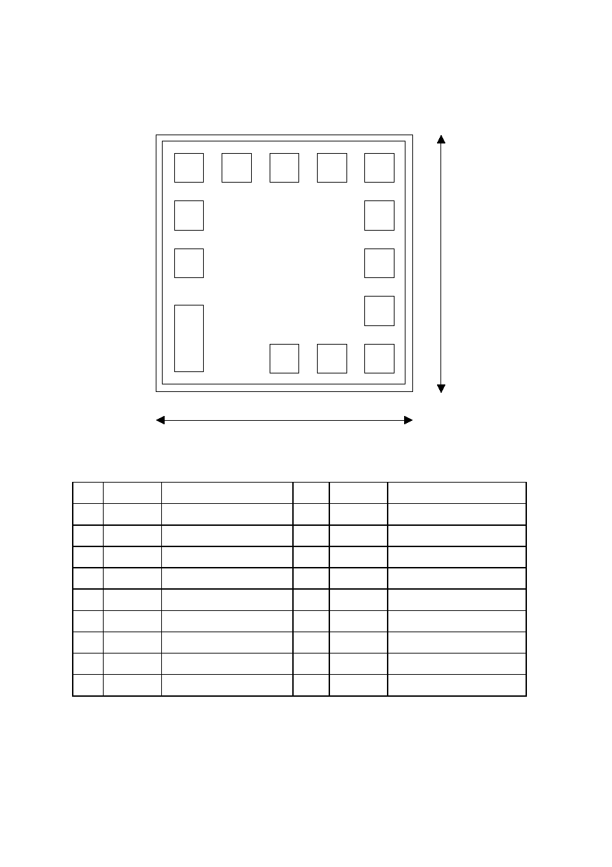
Die Pad Assignment
14
13
12
11
10
9
8
7
6
5
4
3
1
A
O
2
820um
820um
No.
Symbol Center Coordinates (um)
No.
Symbol
Center Coordinates (um)
1 VDD3.3
(75,140)
10 Vss
(395,715)
2 VDD5.0
(395,75)
11 VDD3.3
(235,715)
3 OUTB
(555,75)
12 CAP
(75,715)
4 Vss
(715,75)
13 Vss
(75,555)
5 OUTB
(715,235)
14 IN
(75,395)
6 Vss
(715,395)
7 OUT
(715,555)
8 Vss
(715,715)
O
(0,0)
9 OUT
(555,715)
A
(790,790)