 | –≠–ª–µ–∫—Ç—Ä–æ–Ω–Ω—ã–π –∫–æ–º–ø–æ–Ω–µ–Ω—Ç: F0100505B | –°–∫–∞—á–∞—Ç—å:  PDF PDF  ZIP ZIP |
Features
∑ 1.5k
high transimpedance
∑ 28 dB gain
∑ Low noise (typ.8.2 pA/
Hz@100 MHz)
∑ Typical 2400 MHz O/E bandwidth
∑ Over 25 dB wide dynamic range
∑ 3.3 V or 5.0 V single voltage supply operation
∑ Differential output
Applications
∑ Preamplifier of an optical receiver circuit for OC-48/STM-16 (2.7 Gb/s (FEC available))
Functional Description
The F0100505B is stable GaAs integrated transimpedance amplifier. Typical Applica-
tions are for 2.7 Gb/s (FEC avaiable) optical receiver circuit, for example, OC-48/STM-16,
instrumentation, and measurement applications. The integrated feedback loop design pro-
vides broad bandwidth and stable operation. The F0100505B typically specifies a high
transimpedance of 1.5 k
(RL=50
) at a typical 2400 MHz O/E bandwidth (-3 dB-cutoff
frequency) with a dynamic range of over 25 dB. It also provides a large optical input overload
of more than +1 dBm. Furthermore, it can operate with a low supply voltage of single +3.3 V.
It features a typical dissipation current of 45 mA.
Only chip-shipment is available for all product lineups of GaAs transimpedance amplifi-
ers, because the packaged preamplifier cannot operate with the maximum performance
owing to parasitic element of the package.
02.05.21
Preliminary
Transimpedance Amplifier
F0100505B
3.3 V /5V 2.5 Gb/s NRZ Receiver

3.3 V / 5V 2.5Gb/s Transimpedance Amplifier
F0100505B
Absolute Maximum Ratings
All published data at Ta=25
∞
C unless otherwise indicated. This device isn't guaran-
teed opto-electric characteristics in these ranges. At least, this device isn't broken in these
ranges.
V
SS
=0 V
Recommended Operating Conditions
V
SS
=0 V, unless specified
Parameter
Symbol
Value
Units
Attentions
Supply Voltage
V
DD3.3
-0.3 to +4.0 V
-0.3 to +7.0 V
V
at 3.3 V operation
at 5.0 V operation
Supply Voltage
I
DD5.0
mA
Input Current
Iinpeak
4
mA
Ambient Operating Temperature
Ta
-40 to +90
∞C
Storage Temperature
Tstg
-50 to 125
∞C
-
-
-
Parameter
Symbol
Value
Units
Min.
Typ.
Max.
Supply Voltage
Supply Voltage
3.10
3.60
V
V
4.75
5.25
∞C
Ambient Operating Temperature
Input Capacitance
0
3.30
5.00
25
-
-
85
pF
Attentions
at 3.3 V operation
at 5.0 V operation
at Vb=-2 V*
V
DD3.3
I
DD5.0
Cpd
Ta
0.25
* Vb is the bias between IN and VPD. Show [Test Circuits / 2 ] Block Diagram of F0832483T]

3.3 V / 5V 2.5 Gb/s Transimpedance Amplifier
F0100505B
Electrical Characteristics
Ta=25
∞
C, V
DD3.3
=3.3 V, V
SS
=0, unless specified
* 1 Test circuit is shown [Test Circuits / 1] AC Characteristics].
* 2 Zt(p,n)=10^(S21(p,n)/20
◊
(Ri+50)/2
Optical and Electrical Characteristics
This table values are specified by F0832671T. F0832671T is 2.7 Gb/s (FEC available)
NRZ PIN-PD preamplifier module using F0100505B. Test circuits of F0832671T are shown
in [Test Circuits].
Ta=25
∞
C, V
DD3.3
=3.3 V, V
SS
=0 V, unless specified
* 3 Shown [Test Circuits/3] Optical & Electrical Characteristics].
* 4 Shown [Test Circuits/4] Sensitivity Characteristics].
Parameter
Symbol
Value
Units
Min.
Typ.
Max.
Test Conditions
Transimpedance
O/E High Cut-off Frequency
O/E Low Cut-off Frequency
Equivalent Input Noise
Sensitivity
Overload
Output Impedance
RL=50
, Single-ended
f=100 MHz,
*3
2.66606 Gb/s, PRBS2^23-1,
BER=1E-10,
*4
Ztm
Fcoeh
Fcoel
Inoise
Pin-min
Pin-max
Routm
-
-
-
-
-
+2
-
1.4
2400
17
8.2
-23
-
TBD
-
-
-
-
-
-
-
k
MHz
kHz
pA/
Hz
dBm
dBm
Ztm-3dB,
*3
Cout=470pF
f=100 MHz
No input, f=1 MHz,
*3
Parameter
Symbol
Test Conditions
Value
Units
Min.
Typ.
Max.
Supply Current
I
DD
DC
-
50
-
mA
Gain(positive)
RL=-50
,
Single-ended, *2
RL=-50
,
Single-ended, *2
Cout=470 pF
*1
*1
*1
-
0.96
2.13
-
-
dB
Gain(negative)
Single-ended, f=1 MHz *1
Single-ended, f=1 MHz *1
-
2.04
-
dB
-3dB High Frequency
Cut-off (positive)
-
27.6
-
MHz
-3dB High Frequency
Cut-off (negative)
-
27.4
-
-
MHz
Input Impedance
Output Impedance(positive)
Output Impedance(negative)
-
1130
-
Transimpedance(negative)
Transimpedance(positive)
-
1010
-
-
67
-
Output Voltage(positive)
-
-
59
-
Output Voltage(negative)
-
-
55
1.5
-
Input Voltage
V
i
R
i
R
out
R
out
Z
tp
Z
tn
V
op
V
on
S
21p
S
21n
S
21p
-3dB
S
21p
-3dB
F
cp
F
cn
-
-
AGC time constant
-
1.5
10
-
µ
sec
tagc
f=1 MHz, *1
f=1 MHz, *1
f=1 MHz, *1
k
k
V
V
V

3.3 V / 5V 2.5Gb/s Transimpedance Amplifier
F0100505B
Block Diagram
Cout
CAP
OUT
OUTB
IN
V
DD3.3
VSS
AGC
V
DD5.0
Rf
Symbol
V
DD3.3
V
DD5.0
V
SS
IN
OUT
OUTB
CAP
Description
Supply Voltage for 3.3 V operation, it is not required for 5.0 V operation.
Supply Voltage for 5.0 V operation, For 3.3 V operation, V
DD3.0
must be opened.
Supply Voltage Generally V
SS
is connected to GND.
Input
Non-inverted data output, must be AC coupled.
Inverted data output, must be AC coupled.
Connected to outer capacitance

3.3 V / 5V 2.5 Gb/s Transimpedance Amplifier
F0100505B
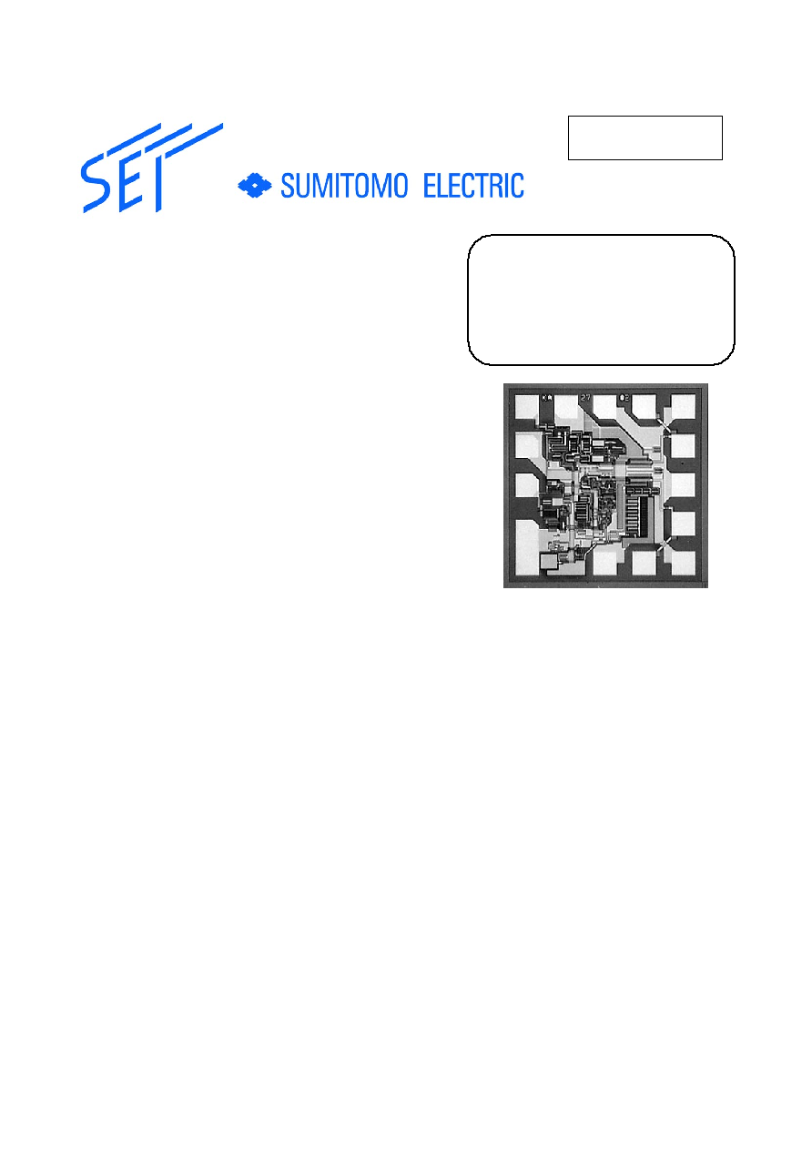
Die Pad Assignments
No.
1
2
3
4
5
6
7
8
9
Symbol
V
DD3.3
V
DD5.0
OUTB
V
SS
OUTB
V
SS
OUT
V
SS
OUT
Center Coordinates (
µ
m)
(75,140)
(395,75)
(555,75)
(715,75)
(715,235)
(715,395)
(715,555)
(715,715)
(555,715)
No.
10
11
12
13
14
O
A
Symbol
V
SS
V
DD3.3
CAP
V
SS
IN
Center Coordinates (
µ
m)
(395,715)
(235,715)
(75,715)
(75,555)
(75,395)
(0,0)
(790,790)
820
µ
m
A
O
1
2
3
4
5
6
7
8
9
10
11
12
13
14
820
µ
m