
Features
∑ Up to 3 Gb/s high speed operation
∑ Positive thermal coefficient of modulation current
∑ Differential ECL compatible interface
∑ -5.2 V single power supply
∑ Up to 50 mA p-p modulation current
∑ Up to 50 mA bias current
∑ Maximum bias current preset control
∑ Low-cost 18-terminal LCC package
Applications
∑ Laser diode driver of an optical transmitter circuit up to 3 Gb/s
Functional Description
The F0513005L is a high performance GaAs integrated laser diode driver for use in an
optical transmitter circuit up to 3 Gb/s NRZ data rate. The F0513005L typically specifies rise
time and fall time of 140 psec (10 % - 90 %). It features single -5.2 V supply operation, 1 to
50 mA presettable bias current and up to 50 mA modulation current while dissipating 650
mW is typical. A choice of three packages are available to match various application re-
quirements: an 18-terminal leadless chip carrier (LCC) called F0513005L, an 18-lead metal-
based flat package (MFP) called F0513005M, and a 20-lead plastic-molded QFP package
called F0513005S.
01.08.28
Laser Diode Driver
3 Gb/s NRZ Data Rate
F0513005L

F0513005L
3 Gb/s Laser Diode Driver
Absolute Maximum Ratings
T
a
= 25
∞
C, unless specified
Recommended Operating Conditions
T
a
= 25
∞
C, V
SS
= - 5.2 V, unless specified
r
e
t
e
m
a
r
a
P
l
o
b
m
y
S
e
u
l
a
V
s
t
i
n
U
e
g
a
t
l
o
V
y
l
p
p
u
S
V
S
S
5
.
0
o
t
7
-
V
n
o
i
t
a
p
i
s
s
i
D
r
e
w
o
P
s
i
d
P
1
W
e
g
a
t
l
o
V
t
u
p
n
I
V
1
N
I
V
,
2
N
I
5
.
0
o
t
3
-
V
e
g
a
t
l
o
V
t
u
p
t
u
O
V
1
T
U
O
V
,
2
T
U
O
5
.
0
o
t
3
-
V
e
g
a
t
l
o
V
l
o
r
t
n
o
C
t
n
e
r
r
u
C
n
o
i
t
a
l
u
d
o
M
V
M
V
S
S
V
o
t
S
S
3
.
1
+
V
g
n
i
t
t
e
S
t
n
e
r
r
u
C
s
a
i
B
m
u
m
i
x
a
M
e
g
a
t
l
o
V
V
B
V
S
S
V
o
t
S
S
1
+
V
e
g
a
t
l
o
V
C
P
A
V
1
C
P
A
V
,
2
C
P
A
5
.
0
o
t
3
-
V
e
r
u
t
a
r
e
p
m
e
T
e
g
a
r
o
t
S
g
t
s
T
5
2
1
+
o
t
5
5
-
C
∞
e
r
u
t
a
r
e
p
m
e
T
g
n
i
t
a
r
e
p
O
t
n
e
i
b
m
A
T
a
0
7
+
o
t
0
-
C
∞
Parameter
Symbol
Value
Units
Min.
Typ.
Max.
Supply Voltage
-5.5
-5.2
-5.0
V
Output Voltage
V
OUT1
, V
OUT2
-2.0
-1.0
0
V
Ambient Operating Temperature
Ta
0
25
70
∞ C
V
SS

3 Gb/s Laser Diode Driver
F0513005L
Electrical Characteristics
T
a
= 25
∞
C, V
SS
= - 5.2 V, unless specified
(1) except modulation current
(2) IMTC = 100
◊
[ I
M
(T
a
= 70
∞
C) - I
M
(T
a
= 0
∞
C) ] / I
M
(T
a
= 25
∞
C) / 70
NOTES:
1. Modulation circuit on: V
IN1
= - 1.7 V, V
IN2
= - 0.9 V
2. Modulation circuit off: V
IN1
= - 0.9 V, V
IN2
= - 1.7 V
3. Bias circuit on: V
APC1
= 0 V, V
APC2
= - 2.5 V
4. Bias circuit off: V
APC1
= - 2.5 V, V
APC2
= 0 V
r
e
t
e
m
a
r
a
P
l
o
b
m
y
S
s
n
o
it
i
d
n
o
C
t
s
e
T
e
u
l
a
V
s
ti
n
U
.
n
i
M
.
p
y
T
.
x
a
M
)
1
(
t
n
e
r
r
u
C
ti
u
c
r
i
C
I
S
S
V
M
V
2
.
5
-
=
B
V
,
V
2
.
5
-
=
-
5
7
0
1
1
A
m
e
g
a
tl
o
V
t
u
p
n
I
V
H
I
e
d
o
M
l
a
it
n
e
r
e
f
fi
D
9
.
0
-
-
7
.
0
-
V
V
L
I
9
.
1
-
-
7
.
1
-
V
t
n
e
r
r
u
C
t
u
p
n
I
I
1
N
I
I
,
2
N
I
V
1
N
I
V
,
2
N
I
V
9
.
1
-
=
0
5
1
-
-
0
5
1
µ
A
t
n
e
r
r
u
C
n
o
it
a
l
u
d
o
M
I
X
A
M
M
V
1
N
I
V
,
V
7
.
1
-
=
2
N
I
V
9
.
0
-
=
V
1
C
P
A
V
,
V
5
.
2
-
=
2
C
P
A
V
0
=
V
M
V
,
V
9
.
3
-
=
B
V
2
.
5
-
=
0
5
-
-
A
m
I
N
I
M
M
V
1
N
I
V
,
V
7
.
1
-
=
2
N
I
V
9
.
0
-
=
V
1
C
P
A
V
,
V
5
.
2
-
=
2
C
P
A
V
0
=
V
M
V
,
V
5
.
2
-
=
B
V
2
.
4
-
=
-
-
1
A
m
I
M
)
2
(
t
n
e
i
c
if
f
e
o
C
l
a
m
r
e
h
T
I
C
T
M
I
M
T
(
A
m
0
5
o
t
5
2
=
a
)
C
∞
5
2
=
T
a
C
∞
0
7
o
t
0
=
0
-
6
.
0
C
∞
/
%
t
n
e
r
r
u
C
s
a
i
B
I
X
A
M
B
V
1
N
I
V
,
V
9
.
0
-
=
2
N
I
V
7
.
1
-
=
V
1
C
P
A
V
,
V
0
=
2
C
P
A
V
5
.
2
-
=
V
M
V
,
V
2
.
5
-
=
B
V
2
.
4
-
=
0
5
-
-
A
m
I
N
I
M
B
V
1
N
I
V
,
V
9
.
0
-
=
2
N
I
V
7
.
1
-
=
V
1
C
P
A
V
,
V
5
.
2
-
=
2
C
P
A
V
0
-
=
V
M
V
,
V
2
.
5
-
=
B
V
2
.
5
-
=
-
-
1
A
m
e
m
i
T
e
s
i
R
r
t
5
2
=
L
R
%
0
9
-
%
0
1
-
-
0
0
2
s
p
e
m
i
T
ll
a
F
f
t
5
2
=
L
R
%
0
9
-
%
0
1
-
-
0
0
2
s
p
F0513005L
3 Gb/s Laser Diode Driver
12
13
14
15
16
18
11
10
9
8
7
6
5
4
3
2
1
17
No.1 LEAD IDENTIFIER
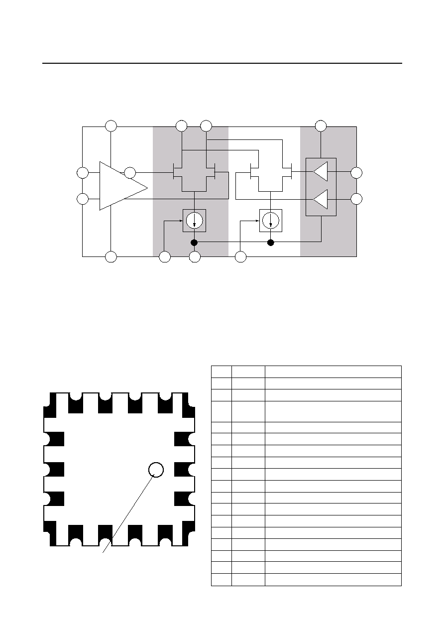
Block Diagram
Pin Assignments (Bottom View)
Pin Descriptions
1
OUT1
Output
2
NC
No Connection
3
V
APC1
APC Signal Input
4
V
B
Maximum Bias Current (I
BMAX
)Setting
Voltage
5
V
SS
Supply Voltage
6
GND
Supply Voltage
7
V
M
Modulation Current Control Voltage
8
V
APC2
APC Reference Voltage
9
NC
No Connection
10
OUT2
Output
11
NC
No Connection
12
V
IN2
Differential Mode Input
13
GND
Supply Voltage
14
NC
No Connection
15
NC
No Connection
16
V
SS
Supply Voltage
17
V
IN1
Differential Mode Input
18
GND
Supply Voltage
VIN2
VIN1
Input
Buffer
Switching
Section
Bias Setting
Section
Level
Shifter
VAPC1
VAPC2
VSS
VM
VB
GND
OUT1 OUT2
VSS
GND
+
-
